
Wafer Level Chip Scale Packaging (WLCSP) Market Insights
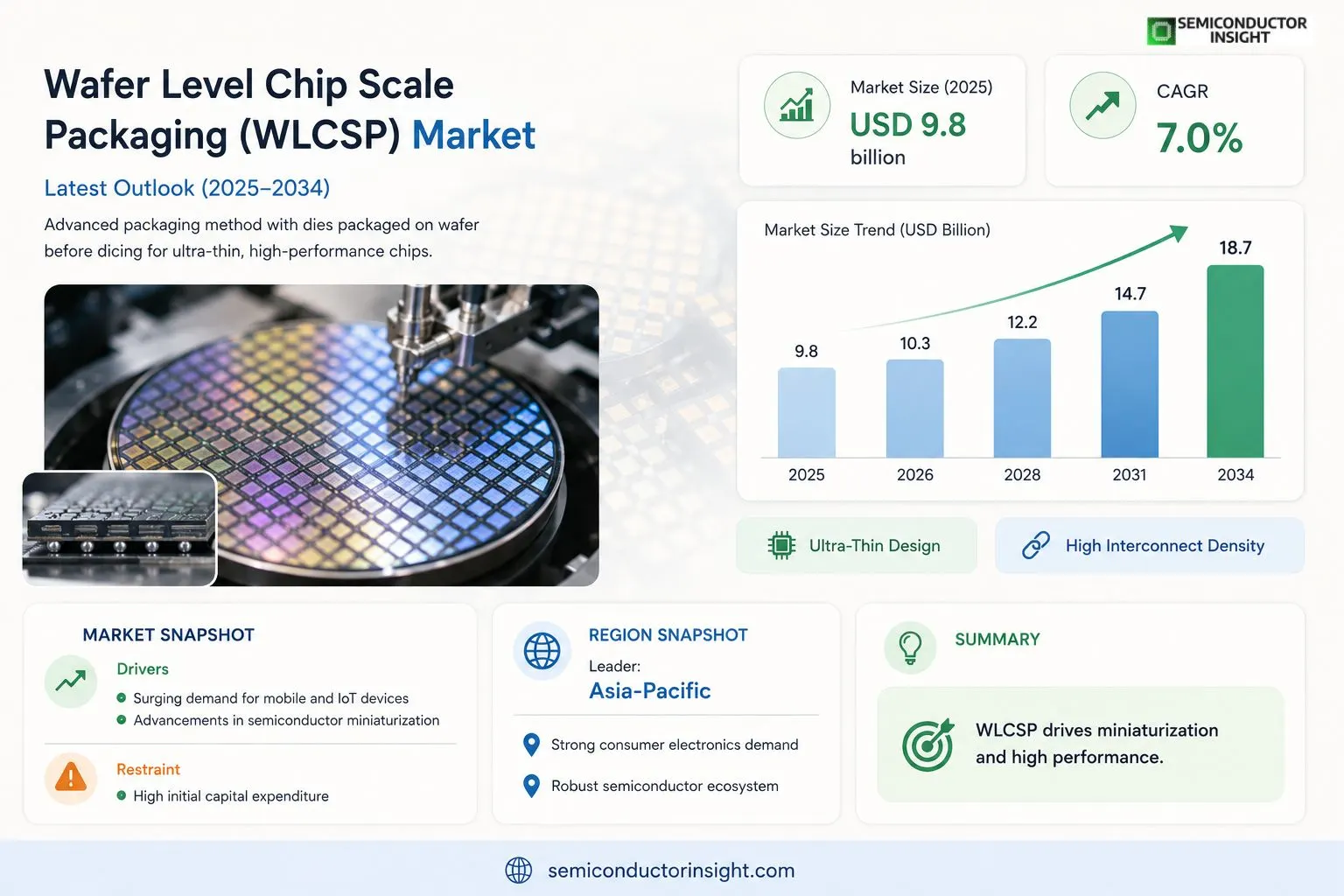
Global Wafer Level Chip Scale Packaging (WLCSP) market size was valued at USD 9.8 billion in 2025. The market is projected to grow from USD 10.3 billion in 2025 to USD 18.7 billion by 2034, exhibiting a CAGR of approximately 7. 0% during the forecast period.
Wafer Level Chip Scale Packaging (WLCSP) is an advanced semiconductor packaging technique where individual dies are packaged directly on the wafer before dicing, delivering ultra‑thin form factors, low parasitic inductance, and high electrical performance while minimizing material usage.
The rapid expansion of mobile devices, wearables, and IoT sensors drives demand for smaller footprints and higher interconnect density,key advantages offered by WLCSP technology.
Furthermore, the shift toward heterogeneous integration and the need for cost‑effective high‑volume production encourage semiconductor manufacturers to adopt wafer‑level solutions.
Key industry players such as ASE Technology Holding, Amkor Technology, STMicroelectronics, and TSMC continue investing in R&D and capacity expansion to meet escalating demand across consumer electronics and automotive sectors.
MARKET DRIVERS
Rapid Expansion of Mobile and IoT Devices
Wafer Level Chip Scale Packaging (WLCSP) Market is being propelled by the surging demand for ultra‑thin smartphones, wearables, and IoT sensors that require high performance in a compact footprint. Manufacturers are shifting to WLCSP to achieve board‑level integration while keeping form‑factor minimal, resulting in an estimated CAGR of about 12% through 2028.
Advancements in Semiconductor Miniaturization
Process innovations such as finer lithography and advanced redistribution layers enable higher I/O density on wafers, making WLCSP an attractive choice for high‑frequency applications like 5G RF front‑ends and automotive ADAS modules. These technical gains translate into cost savings of up to 15% compared with traditional flip‑chip solutions.
➤ Analysts estimate that by 2025, WLCSP will account for roughly 30% of total chip‑scale packaging shipments worldwide.
In addition, the growing emphasis on sustainability drives design teams toward wafer‑level approaches that reduce material waste and simplify supply chains, further reinforcing market momentum.
MARKET CHALLENGES
Technical Complexity and Yield Management
Implementing WLCSP demands precise alignment and stringent contamination control; even minor process deviations can cause yield losses that offset its cost advantages. Companies investing in advanced inspection tools are better positioned to mitigate these risks.
Other Challenges
Limited Availability of Skilled Workforce
The specialized nature of wafer‑level processes requires engineers with niche expertise, creating a talent bottleneck that can slow adoption rates.Moreover, the need for extensive reliability testing,especially for automotive and medical applications,adds time and expense, compelling firms to balance speed with robustness.
MARKET RESTRAINTS
High Initial Capital Expenditure
Establishing a production line for Wafer Level Chip Scale Packaging (WLCSP) Market involves sizable upfront investments in cleanroom facilities, wafer‑handling robotics, and metrology equipment. Smaller players often face barriers to entry due to these capital constraints.Additionally, the long payback period,typically 3 to 5 years,can deter investment, especially in regions with lower manufacturing incentives.
MARKET OPPORTUNITIES
Emergence of 5G and Edge Computing
The rollout of 5G networks and the shift toward edge computing create a strong demand for high‑frequency, low‑latency components. WLCSP’s minimal parasitic inductance and superior RF performance make it well‑suited for these applications, opening new revenue streams for early adopters.Furthermore, the automotive sector’s transition to autonomous driving systems presents a sizable opportunity, as WLCSP can deliver the required miniaturization and reliability for sensors, radar, and lidar modules.
Wafer Level Chip Scale Packaging (WLCSP) Market Trends
Growth Driven by Mobile, Wearables and IoT Sensors
The rapid expansion of consumer electronics, especially smartphones, wearables, and IoT sensors, is creating a persistent demand for ultra‑thin form factors and high interconnect density. Wafer Level Chip Scale Packaging delivers these attributes by eliminating traditional substrate steps, which reduces parasitic inductance and enables tighter board layouts. As manufacturers prioritize price‑per‑function, the ability of WLCSP to minimize material usage while maintaining electrical performance has positioned it as a preferred solution for next‑generation devices that require compactness without compromising reliability.
Other Trends
Heterogeneous Integration
The industry’s shift toward heterogeneous integration is amplifying the relevance of wafer‑level solutions. By mounting multiple functional dies on a single wafer, manufacturers achieve system‑in‑package architectures that combine logic, memory, and sensor functions. This approach lowers assembly steps and supports high‑volume production, aligning with cost‑efficiency goals. Key players are expanding R&D pipelines to refine alignment techniques and to enhance thermal management, ensuring that heterogeneous designs meet the stringent reliability standards of both consumer and industrial markets.
Automotive and High‑Performance Applications
Automotive electronics, ranging from advanced driver‑assistance systems to infotainment modules, are increasingly adopting Wafer Level Chip Scale Packaging to meet strict weight and space constraints while delivering robust electrical performance. The technology’s low profile and superior signal integrity are advantageous for radar, LIDAR, and power management modules that operate under harsh thermal cycles. Simultaneously, high‑performance computing segments are leveraging WLCSP to reduce latency in high‑frequency interconnects, supporting the growth of edge AI devices that demand both speed and miniaturization.
COMPETITIVE LANDSCAPEKey Industry Players
Wafer Level Chip Scale Packaging (WLCSP) Market Competitive Overview
Wafer Level Chip Scale Packaging (WLCSP) Market is anchored by a handful of large‑scale manufacturers that command the majority of capacity and R&D spend. ASE Technology Holding, Amkor Technology, TSMC, and STMicroelectronics together account for roughly 60 % of global wafer‑level output, leveraging expansive fab networks and deep integration capabilities to serve high‑volume consumer electronics and automotive clients. Their strategic investments in advanced redistribution layers, fan‑in/fan‑out architectures, and cost‑efficient high‑throughput processes create entry barriers for smaller entrants and reinforce a tiered market structure where premium‑price contracts are concentrated among these industry leaders.
Beyond the core quartet, a broader cohort of niche and diversified players is expanding the WLCSP ecosystem. Samsung Electronics, Intel, NXP Semiconductors, Texas Instruments, Broadcom, Infineon Technologies, Renesas Electronics, and GlobalFoundries target specific segments such as IoT sensors, wearables, and automotive safety modules, often partnering with fabless designers to offer customized footprint solutions. Their agility in adopting heterogeneous integration, thin‑form‑factor designs, and low‑parasitic interconnects complements the larger players, fostering a competitive environment that drives incremental innovation and price compression across the value chain.
List of Key Wafer Level Chip Scale Packaging (WLCSP) Companies Profiled
- ASE Technology Holding
- Amkor Technology
- TSMC
- Samsung Electronics
- STMicroelectronics
- Intel
- NXP Semiconductors
- Texas Instruments
- Broadcom
- Infineon Technologies
- Renesas Electronics
- GlobalFoundries
Segment Analysis:
| Segment Category | Sub-Segments | Key Insights |
| By Type |
|
Flip‑Chip WLCSP
|
| By Application |
|
Mobile smartphones
|
| By End User |
|
Consumer electronics
|
| By Integration Approach |
|
Heterogeneous integration
|
| By Device Category |
|
Wearables & AR/VR headsets
|
Regional Analysis: Asia-Pacific
Asia-Pacific Region
China’s significant investment in its domestic semiconductor industry is propelling WLCSP demand. The government’s focus on self-sufficiency in key technologies is driving adoption across various sectors, contributing to a dynamic and competitive market.
Taiwan remains a global leader in semiconductor manufacturing and WLCSP technology development. The region’s established ecosystem and strong focus on innovation position it as a key player in the WLCSP market, particularly for high-performance applications.
South Korea’s strong automotive industry is a major driver of WLCSP adoption. The increasing demand for advanced driver-assistance systems (ADAS) and electric vehicles (EVs) is boosting the need for miniaturized and high-reliability WLCSP solutions.
Japan’s robust industrial sector presents a steady demand for WLCSP in various applications, including industrial automation, robotics, and medical devices. Emphasis on miniaturization and efficiency drives the technology adoption.
North America
North America represents a mature market for WLCSP, driven by the presence of major semiconductor manufacturers and a strong focus on advanced technology. The demand is concentrated in high-end applications such as aerospace, defense, and high-performance computing. Ongoing research and development efforts are focused on enhancing WLCSP performance and reliability for these demanding sectors. The market is characterized by a relatively high adoption rate and a focus on specialized solutions.
Europe
Europe’s WLCSP market is experiencing moderate growth, driven by increasing demand from the automotive, consumer electronics, and industrial sectors. Government initiatives promoting smart manufacturing and digital transformation are contributing to market expansion. Emphasis on energy efficiency and miniaturization is a key driver for WLCSP adoption in European industries. The region is witnessing a growing interest in WLCSP for IoT devices and wearable technologies.
South America
South America presents a nascent market for WLCSP with significant growth potential. The increasing adoption of smartphones, automotive electronics, and industrial automation is driving demand. The market is still relatively fragmented, with opportunities for new entrants and innovative solutions. The growing focus on connectivity and digital infrastructure is expected to accelerate WLCSP adoption in the region.
Middle East & Africa
The Middle East & Africa region is an emerging market with growing demand for WLCSP, primarily driven by infrastructure development, urbanization, and increasing investments in the automotive and telecommunications sectors. The region’s focus on smart cities and industrial growth is expected to further fuel WLCSP adoption. The market is characterized by increasing disposable incomes and a growing consumer electronics market.
Report Scope
This market research report provides a comprehensive analysis of the Wafer Level Chip Scale Packaging (WLCSP) Market , covering the forecast period 2026–2034. It offers detailed insights into market dynamics, technological advancements, competitive landscape, and key trends shaping the industry.
Key focus areas of the report include:
- Market Overview: The report begins with an overview outlining its current market scenario, key growth indicators, and industry transformation drivers. It discusses macroeconomic factors, demand–supply balance, regulatory landscape, and the strategic role of semiconductors in powering advancements across industries such as automotive, telecommunications, consumer electronics, and industrial automation.
- Market Size & Forecast: Historical data and future projections for revenue, unit shipments, and market value across major regions and segments.
- Segmentation Analysis: Detailed breakdown by product type, technology, application, and end-user industry to identify high-growth segments and investment opportunities.
- Regional Insights: Insights into market performance across North America, Europe, Asia-Pacific, Latin America, and the Middle East & Africa, including country-level analysis where relevant.
- Competitive Landscape: Profiles of leading market participants, including their product offerings, R&D focus, manufacturing capacity, pricing strategies, and recent developments such as mergers, acquisitions, and partnerships.
- Technology Trends & Innovation: Assessment of emerging technologies, integration of AI/IoT, semiconductor design trends, fabrication techniques, and evolving industry standards.
- Market Drivers & Restraints: Evaluation of factors driving market growth along with challenges, supply chain constraints, regulatory issues, and market-entry barriers.
- Stakeholder Insights: Insights for component suppliers, OEMs, system integrators, investors, and policymakers regarding the evolving ecosystem and strategic opportunities.
Primary and secondary research methods are employed, including interviews with industry experts, data from verified sources, and real-time market intelligence to ensure the accuracy and reliability of the insights presented.
FREQUENTLY ASKED QUESTIONS:
What is the current market size of Wafer Level Chip Scale Packaging (WLCSP) Market?
-> Wafer Level Chip Scale Packaging (WLCSP) Market was valued at USD 9.8 billion in 2025 and is expected to reach USD 18.7 billion by 2034, with a CAGR of approximately 7.0% during the forecast period.
Which key companies operate in Wafer Level Chip Scale Packaging (WLCSP) Market?
-> Key players include ASE Technology Holding, Amkor Technology, STMicroelectronics, and TSMC, among others.
What are the key growth drivers?
-> Key growth drivers include the rapid expansion of mobile devices, wearables, and IoT sensors, demand for smaller footprints and higher interconnect density, and the shift toward heterogeneous integration and cost‑effective high‑volume production.
Which region dominates the market?
-> The reference does not specify a single dominant region; however, demand is strong globally across major semiconductor manufacturing hubs.
What are the emerging trends?
-> Emerging trends include heterogeneous integration, advanced wafer‑level packaging techniques, and increased focus on cost‑effective high‑volume production for consumer electronics and automotive applications.

Get Sample Report PDF for Exclusive Insights
Report Sample Includes
- Table of Contents
- List of Tables & Figures
- Charts, Research Methodology, and more...
 Download Sample Report PDF

