
Key Statistics
Key Takeaways
- Semiconductor Lithography Machine is the highest-value equipment category because leading-edge lithography tools carry exceptionally high capital intensity and determine patterning capability, while Deposition/Thin Film Equipment and advanced etch are among the strongest growth areas as gate-all-around logic, HBM and 3D device structures add process steps.
- Foundry and Logic Equipment is the largest application segment. SEMI’s 2025 year-end outlook placed foundry and logic WFE sales at US$ 66.6 billion in 2025, with advanced-node investment supporting continued growth; DRAM is one of the fastest-growing applications as HBM-related capacity and technology migrations accelerate.
- Asia Pacific is the largest regional demand base because China, Korea, Taiwan and Japan together account for the majority of global fab-equipment spending. In SEMI’s March 2025 forecast, China alone was expected to spend US$ 38 billion in 2025, followed by Korea and Taiwan at about US$ 21.5 billion and US$ 21 billion.
- The Americas are the fastest-growing investment region in the current cycle. SEMI projected front-end fab equipment spending in the Americas to rise from US$ 14 billion in 2025 to US$ 20 billion in 2026, while U.S. CHIPS awards support large new fabs from TSMC, Intel, Samsung, Micron and other device makers.
- AI infrastructure is the dominant near-term demand catalyst. SEMI’s July 2026 forecast raised WFE sales to US$ 143.9 billion in 2026, up 23.1% year over year, with leading-edge logic, advanced memory and HBM-related DRAM investment driving the revision.
Wafer Fab Equipment (WFE) Market Overview
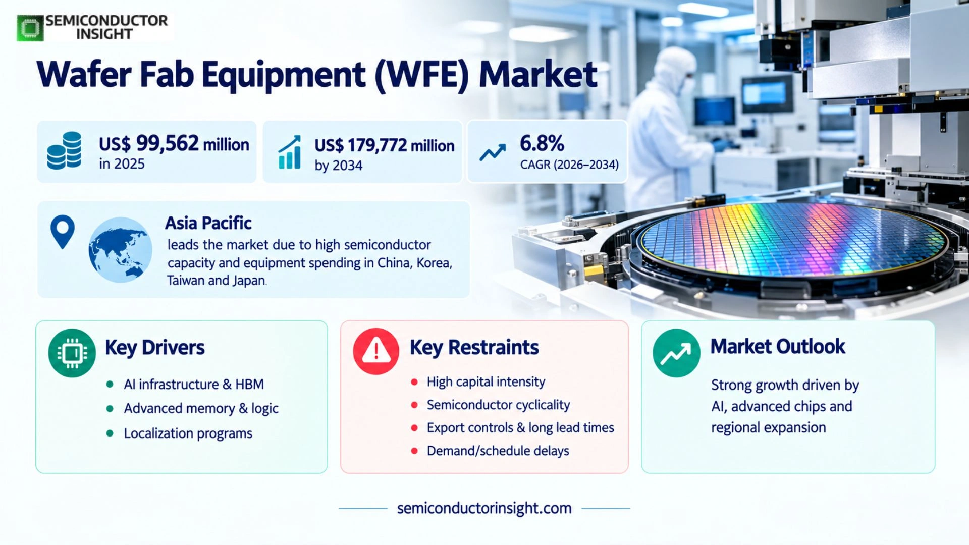
Wafer Fab Equipment (WFE) market is rebased to US$ 99,562 million in 2025, with an estimated US$ 106,318 million in 2026, and is projected to reach US$ 179,772 million by 2034. The anchor-implied compound rate is 6.8% for 2026–2034. Asia Pacific is the largest regional market because semiconductor manufacturing capacity and equipment spending are concentrated in China, Korea, Taiwan and Japan.
Wafer fab equipment comprises the capital tools used to transform a bare semiconductor wafer through repeated cycles of film formation, lithography, pattern transfer, implantation, thermal treatment, planarization, cleaning and process control before the wafer leaves front-end fabrication. The source report defines nine WFE categories: semiconductor etching equipment, deposition/thin-film equipment, front-end inspection and metrology, coater and developer, lithography machines, cleaning equipment, ion implanters, CMP equipment and heat-treatment equipment.
The market is unusually sensitive to technology transitions because a new transistor architecture or memory structure does not simply replace one tool with another; it can add deposition, etch, metrology and cleaning steps across the entire process flow. SEMI’s July 2026 outlook projected WFE sales of US$ 143.9 billion in 2026, up 23.1% year over year, after a record US$ 116.9 billion in 2025. The association attributed the acceleration to leading-edge logic, advanced memory and HBM-related DRAM investment. SEMI source.
Fab construction and equipment installation are also becoming more geographically distributed. SEMI’s March 2025 World Fab Forecast expected front-end fab equipment investment of US$ 110 billion in 2025 and US$ 130 billion in 2026, with about 50 new fabs expected to come online across those two years. China, Korea, Taiwan and the Americas were the largest investment destinations, reinforcing the link between regional capacity policy and WFE order books. SEMI source.
The commercial structure is therefore defined by long tool-development cycles, high customer qualification barriers, a small number of suppliers in several critical process steps, and demand that can change sharply when device makers accelerate or delay fab projects. Advanced-node transitions create the highest-value opportunities, but mature-node capacity remains strategically important because analog, power, automotive and industrial semiconductors continue to require 200mm and mature 300mm production. Suppliers need both technology leadership and the service infrastructure to sustain installed tools for many years.
Base year: 2025 · Estimated year: 2026 · Forecast period: 2026–2034 · Historical source anchor: 2023 · Values in US$ million
Segment Analysis: By Type
The source page segments WFE into Semiconductor Etching Equipment, Deposition/Thin Film Equipment, Semiconductor Front-end Inspection & Metrology, Semiconductor Coater & Developer, Semiconductor Lithography Machine, Semiconductor Cleaning Equipment, Ion Implanter, CMP Equipment and Heat Treatment Equipment. Lithography is the highest-value category, while deposition and etch gain process intensity as leading-edge logic and advanced memory add layers, selective material removal and tighter process windows.
| Type | Function | Market position |
|---|---|---|
| Semiconductor Etching Equipment | Transfers patterned features into films and substrates using plasma or wet processes, with critical roles in high-aspect-ratio memory structures and advanced logic. | High-growth core category. More complex 3D NAND, GAA logic and advanced memory increase etch depth, selectivity and uniformity requirements. Supplier competition centers on plasma control, chamber productivity, process repeatability and the ability to co-optimize etch with deposition and cleaning steps. |
| Deposition/Thin Film Equipment | Deposits conductive, dielectric and barrier layers using CVD, PVD, ALD, epitaxy and related processes. | One of the fastest-expanding categories. GAA transistors, advanced interconnects and HBM-related process flows add more conformal and highly controlled films. Equipment vendors gain when device structures become three-dimensional because the number and precision of film steps increase even without proportional wafer-start growth. |
| Semiconductor Front-end Inspection & Metrology | Measures dimensions, film properties and defects to control yield across lithography, etch, deposition and other process steps. | Strategic high-value category. Shrinking process windows increase the cost of undetected defects and create demand for optical, e-beam and computational process-control tools. KLA, Hitachi High-Tech, Onto Innovation and Lasertec compete across distinct defect and metrology niches. |
| Semiconductor Coater & Developer | Applies photoresist and develops exposed patterns before etch or other pattern-transfer steps. | Essential lithography companion segment. Demand tracks wafer-layer count and lithography intensity, with Tokyo Electron and SCREEN strong in integrated track systems. Advanced nodes demand tighter resist uniformity, contamination control and integration with increasingly expensive exposure tools. |
| Semiconductor Lithography Machine | Projects circuit patterns onto resist-coated wafers using DUV, EUV or other exposure technologies. | Highest-value category. Extreme tool complexity, very high selling prices and leading-edge dependence make lithography a disproportionate share of advanced-node capital spending. ASML dominates EUV, while Canon and Nikon remain relevant in selected DUV and mature-node applications. |
| Semiconductor Cleaning Equipment | Removes particles, residues and contaminants between process steps using wet and dry cleaning technologies. | Process-step intensity rises with more complex device flows. Cleaning is a yield-enabling category because contamination tolerance tightens as features shrink. SCREEN, Tokyo Electron, Lam Research and ACM Research compete through single-wafer productivity, chemistry control and advanced cleaning sequences. |
| Ion Implanter | Introduces controlled dopants into semiconductor materials to modify electrical properties at defined depths and concentrations. | Specialized category with high qualification barriers. Demand follows logic, power and specialty device process changes, while tool value depends on beam control, dose accuracy and throughput. Axcelis is a major specialist in this segment. |
| CMP Equipment | Planarizes wafer surfaces through chemical-mechanical polishing to maintain flatness for subsequent layers. | Critical for multilayer logic and memory. More interconnect layers and advanced packaging-adjacent wafer processes increase planarization requirements. Applied Materials, Ebara and Hwatsing are central suppliers, with consumables and process integration creating recurring value around the installed tool base. |
| Heat Treatment Equipment | Performs oxidation, diffusion, annealing and other thermal processes using furnaces or rapid thermal systems. | Mature but indispensable category. Growth is linked to device architecture transitions, dopant activation and film-property requirements rather than simple wafer capacity. Kokusai Electric and other thermal-processing specialists compete on uniformity, contamination control, batch productivity and advanced thermal budgets. |
Pricing and process-intensity dynamics
WFE pricing spans an unusually wide range because a high-volume cleaning tool, a batch furnace, an ion implanter and an EUV lithography system solve fundamentally different process problems. Revenue growth therefore reflects both tool counts and mix. Leading-edge technology transitions can increase spending without equivalent wafer-capacity growth when process complexity adds deposition, etch, metrology and patterning steps. This process-intensity effect is one of the main reasons AI and HBM investment can disproportionately expand equipment demand.
Segment Analysis: By Application
By application, the source page segments demand into Foundry and Logic Equipment, NAND Equipment, DRAM Equipment and Others. Foundry and Logic is the largest application, while DRAM is a major high-growth area because HBM and advanced memory require new capacity and repeated technology migrations. NAND spending is more cyclical but benefits when layer-count transitions restart after periods of supply discipline.
| Application | Demand characteristics |
|---|---|
| Foundry and Logic Equipment | Largest application. Purchases are triggered by leading-edge node ramps, new fab shells, technology migration and capacity additions for AI accelerators, high-performance computing and premium mobile processors. SEMI projected foundry and logic WFE sales of US$ 66.6 billion in 2025, with continued growth through 2027 as advanced nodes and new device architectures expand. |
| NAND Equipment | Highly cyclical and layer-transition driven. Spending rises when flash producers move to higher layer counts or restore capacity investment after inventory corrections. High-aspect-ratio etch, deposition and process control are especially important because 3D NAND scales vertically rather than primarily through lateral shrink. |
| DRAM Equipment | Fast-growing AI-linked application. HBM demand increases both DRAM wafer investment and process complexity, while technology migrations require new deposition, etch, lithography, metrology and cleaning capability. SEMI’s 2026 outlook identified advanced memory and HBM-related DRAM as a central reason for the sharp upward revision in WFE spending. |
| Others | Includes analog, power, discrete, specialty and other device categories outside the three principal groups. Demand often uses mature nodes and 200mm capacity, producing steadier but lower-ASP equipment requirements. Automotive electrification, industrial electronics and power-management needs can support targeted investments even when leading-edge logic cycles dominate headline spending. |
Application spending confirms the AI-led mix shift
SEMI’s December 2025 year-end forecast put foundry and logic WFE sales at US$ 66.6 billion in 2025, while its July 2026 update raised overall 2026 WFE sales to US$ 143.9 billion. The most important change is mix: advanced logic and HBM-related memory carry greater equipment intensity than many mature-node applications, so suppliers exposed to deposition, etch, lithography and process control can grow faster than wafer volumes alone would suggest. SEMI 2025 and SEMI 2026.
Regional Analysis
Asia Pacific is the largest WFE market because China, Korea, Taiwan and Japan collectively host the majority of global wafer-fabrication capacity and current equipment investment. The Americas are the fastest-growing regional investment market in the near term as U.S. CHIPS-supported fabs move from construction into equipment installation. Europe remains strategically important in specialty manufacturing and equipment supply, while Southeast Asia and Middle East investment is more selective.
How does regional WFE demand differ?
Regional demand follows fab location and technology mix rather than end-product consumption. China buys heavily across mature and increasingly advanced process capacity; Korea is memory-intensive; Taiwan is dominated by leading-edge foundry investment; the Americas are in a localization-driven build cycle; Europe combines automotive, power and specialty semiconductors with strategic new fabs; and Southeast Asia adds selected front-end capacity alongside a larger back-end ecosystem. Supplier access also depends on export controls, local service capability and qualification at each device maker.
| Region | Position | Growth outlook | Demand profile | What decides supplier selection |
|---|---|---|---|---|
| Asia Pacific | Largest | High but mixed by country | Foundry, memory and mature-node expansion | Process leadership, installed-base service, export eligibility, local field engineers and tool productivity. |
| North America | Fastest near-term growth | Very high | Localization and leading-edge fab build-out | Technology qualification, domestic service capacity, CHIPS project schedules and ability to support advanced nodes. |
| Europe | Strategic mid-sized | Moderate | Automotive, power, specialty and selected leading-edge expansion | Energy efficiency, specialty-process capability, local support and compatibility with EU industrial-policy projects. |
| Southeast Asia | Smaller but expanding | Selective | New front-end projects plus adjacent packaging ecosystem | Cost, local service, project execution and suitability for mature or specialty process nodes. |
| Middle East & Others | Early-stage | Project dependent | Strategic localization and greenfield initiatives | Government financing, technology transfer, skilled workforce, infrastructure and supplier willingness to support new ecosystems. |
Detailed Regional Market Analysis
Key WFE Manufacturers and Competitive Landscape
The WFE market is concentrated at the process-step level even though the full source company list is long. ASML dominates advanced lithography; Applied Materials, Tokyo Electron and Lam Research span multiple deposition, etch and related categories; KLA leads critical process control; SCREEN is strong in cleaning and coater/developer systems; and specialist suppliers hold defensible positions in ion implant, CMP, thermal processing, metrology, epitaxy and regional equipment segments.
Competition is shaped by qualification rather than ordinary product substitution. A semiconductor manufacturer does not switch a critical process tool solely because a competitor offers a lower price; the replacement must achieve process performance, yield, uptime and integration targets across a large installed flow. That qualification burden creates durable market positions for incumbent suppliers and turns field service, applications engineering, spare parts and software into a significant part of the competitive moat.
Leading suppliers increasingly compete across adjacent process steps because transistor and memory architectures require co-optimization. Deposition and etch recipes interact, metrology controls both, and cleaning determines whether subsequent layers remain defect-free. A vendor with a broad installed base can use process data and customer relationships to expand into adjacent applications, but specialization still wins where physics, optics or beam technology creates a uniquely difficult barrier, as in EUV lithography or ion implantation.
Chinese suppliers are expanding most rapidly in mature and selected advanced process categories as domestic fabs localize equipment procurement. NAURA, AMEC, ACM Research, Piotech, Hwatsing, Kingsemi and other firms compete across etch, deposition, cleaning, CMP, coating and related tools. Their opportunity is enlarged by local customer access and policy support, but advanced process adoption still depends on yield performance, repeatability and installed-base service rather than on domestic origin alone.
The source page’s competitor list also includes companies whose primary exposure is adjacent to classic front-end WFE, including major test or back-end suppliers. For market analysis, the list is retained exactly in the report scope, while the competitive tiering emphasizes suppliers with defensible front-end wafer-fabrication tool positions. This distinction matters because semiconductor equipment revenue cannot automatically be treated as WFE revenue when a company’s portfolio spans test, packaging or other adjacent categories.
| Competitive tier | Representative companies | Basis of competition |
|---|---|---|
| Broad front-end leaders | Applied Materials; Tokyo Electron; Lam Research | Multi-process portfolios, installed-base scale, advanced-node co-optimization, global field service and deep foundry/memory qualification. |
| Critical technology leaders | ASML; KLA; SCREEN; ASM International; Hitachi High-Tech | Dominant or strong positions in lithography, process control, cleaning/coating, deposition and metrology where technical barriers and qualification are exceptionally high. |
| Specialist process suppliers | Axcelis; Ebara; Kokusai Electric; Onto Innovation; Lasertec; Aixtron; Veeco; Canon; Nikon | Focused technology leadership in implant, CMP, thermal processing, inspection/metrology, epitaxy or selected lithography segments. |
| China-based challengers | NAURA; AMEC; ACM Research; Piotech; Hwatsing; Kingsemi; Beijing E-Town Semiconductor Technology; Shanghai Micro Electronics Equipment | Localization, cost, domestic customer access and improving process capability across mature and increasingly advanced nodes. |
| Broader source-page profiled set | Advantest; Teradyne; DISCO and other listed companies | Retained because the report page profiles them, although some revenue is more strongly associated with test, back-end or adjacent semiconductor equipment categories. |
Companies profiled in the report
- ASML
- Applied Materials, Inc. (AMAT)
- TEL (Tokyo Electron Ltd.)
- Lam Research
- KLA Pro Systems
- SCREEN
- NAURA
- Advantest
- ASM International
- Hitachi High-Tech Corporation
- Teradyne
- Lasertec
- DISCO Corporation
- Canon U.S.A.
- Nikon Precision Inc
- SEMES
- Ebara Technologies, Inc. (ETI)
- Axcelis Technologies Inc
- AMEC
- Kokusai Electric
- Beijing E-Town Semiconductor Technology
- Onto Innovation
- Aixtron
- NuFlare Technology, Inc.
- ACM Research
- Veeco
- Wonik IPS
- Piotech, Inc
- Hwatsing Technology
- SUSS MicroTec REMAN GmbH
- ULVAC TECHNO, Ltd.
- Kingsemi
- Eugene Technology
- PSK Group
- Jusung Engineering
- Oxford Instruments
- Skyverse Technology
- PNC Technology Group
- TES CO., LTD
- Samco Inc.
- Wuhan Jingce Electronic Group
- Plasma-Therm
- Grand Process Technology
- Advanced Ion Beam Technology, Inc. (AIBT)
- Skytech Group
- CVD Equipment
- RSIC scientific instrument (Shanghai)
- GigaLane
- Shanghai Micro Electronics Equipment
WFE Production Capacity Analysis
WFE production capacity is constrained less by factory floor space than by precision supply chains, specialist optics and mechatronics, long-lead subassemblies, highly skilled engineering labor and the time required to qualify complex tools. The most critical suppliers operate global manufacturing networks but maintain substantial technology concentration in the United States, Netherlands, Japan and selected Asian hubs. Capacity expansion therefore requires both physical assembly investment and upstream supplier scaling.
Lithography is the clearest example of technology-constrained capacity. Advanced scanners depend on highly specialized optics, light sources, stages, vacuum systems and precision components that cannot be replicated quickly by adding generic assembly lines. Etch, deposition and process-control equipment also require sophisticated subsystems, but their supply chains are broader. The commercial consequence is that lead times can remain elevated during simultaneous fab ramps even when headline equipment-company factory utilization appears manageable.
Field-service capacity is effectively part of production capacity because an installed WFE tool cannot generate customer value without qualification, process recipes, uptime support and spare parts. New regional fabs in the United States and Europe therefore require equipment vendors to add local application engineers, service technicians and logistics inventory before the tools arrive. A supplier that sells too far ahead of its service footprint risks delayed qualification and lower customer productivity.
SEMI’s March 2025 forecast expected approximately 50 new fabs to come online across 2025 and 2026, while its April 2026 300mm outlook raised projected equipment spending to US$ 133 billion in 2026 and US$ 151 billion in 2027. Simultaneous projects intensify competition for critical subassemblies and engineers because multiple regions are trying to install advanced capacity at the same time. SEMI 2025 and SEMI 2026.
Mature-node equipment introduces a different capacity dynamic. Some 200mm fabs use refurbished tools because new production of older platforms is limited and process recipes are deeply qualified on existing equipment families. SEMI’s 2026 200mm outlook tracked more than 350 fabs and production lines and projected 7.7 million wafers per month of installed capacity. Refurbishment availability, spare parts and obsolescence management therefore remain commercially important alongside new-tool production.
WFE Market Dynamics: Drivers, Restraints and Opportunities
WFE demand is accelerating because AI infrastructure, leading-edge logic, HBM and advanced memory are increasing both wafer capacity and process complexity. Localization programs add a second growth engine by replicating manufacturing ecosystems across regions. The main restraints are extreme capital intensity, semiconductor cyclicality, export controls, qualification lead times and the possibility that device makers delay equipment installation when end-market demand or fab schedules change.
MARKET DRIVERS
Drivers Impact Analysis*
| Market factor | (~) % Impact on CAGR Forecast* | Commercial interpretation |
|---|---|---|
| AI and leading-edge logic investment | +2.0% | Adds advanced-node capacity and increases lithography, etch, deposition, metrology and cleaning intensity. |
| HBM and advanced DRAM expansion | +1.4% | Raises memory equipment spending through both capacity additions and technology migration. |
| Regional fab localization | +1.0% | Replicates production infrastructure in the U.S., Europe and other regions rather than relying only on existing Asian clusters. |
| Process complexity and 3D architectures | +0.8% | Adds more material layers, patterning steps and process-control requirements per wafer. |
AI resets the scale of equipment investment
SEMI’s July 2026 mid-year forecast projects WFE sales of US$ 143.9 billion in 2026, up 23.1% year over year, with continued expansion in 2027 and 2028. The association specifically attributes the stronger trajectory to leading-edge logic, advanced memory and HBM-related DRAM investment. AI therefore affects WFE through both more wafer capacity and greater process intensity per wafer. SEMI source.
HBM turns memory into an equipment-growth engine
HBM requires advanced DRAM technology, high performance and tight yield control, which increases demand for deposition, etch, lithography, metrology and cleaning. Unlike a simple commodity-memory recovery, the HBM cycle is tied to AI accelerator architectures and packaging constraints, making process migration as important as unit demand. Equipment suppliers with qualified advanced-memory applications can therefore capture disproportionate value from each new capacity phase.
Fab regionalization duplicates capital infrastructure
U.S. CHIPS projects illustrate how industrial policy creates WFE demand beyond the traditional cost-minimizing geography. TSMC’s Arizona plan exceeds US$ 65 billion, Intel’s supported U.S. investment approaches US$ 90 billion by decade-end, and Samsung’s Texas plan exceeds US$ 37 billion. Each greenfield fab requires a largely new tool set rather than reallocating an existing one. U.S. Commerce.
Gate-all-around and 3D structures add process steps
The semiconductor industry can no longer scale only by shrinking planar dimensions. Gate-all-around transistors, backside power delivery, 3D NAND and advanced memory architectures use more complex material stacks and three-dimensional structures. That creates additional opportunities for atomic-layer deposition, selective etch, advanced metrology and cleaning. Revenue therefore grows not only when fabs add wafer starts but also when each wafer requires more equipment-intensive processing.
MARKET RESTRAINTS
Restraints Impact Analysis*
| Market factor | (~) % Impact on CAGR Forecast* | Commercial interpretation |
|---|---|---|
| Semiconductor capital-spending cyclicality | -1.3% | Customer utilization, inventory corrections and project timing can rapidly change equipment order schedules. |
| Export controls and geopolitical restrictions | -0.9% | Limit addressable customers or tool configurations for advanced equipment and create compliance uncertainty. |
| Extreme tool and fab capital intensity | -0.7% | Raises hurdle rates for greenfield projects and concentrates advanced-node investment among a small number of device makers. |
| Qualification and long lead times | -0.5% | Slow supplier switching and can delay revenue recognition even when strategic demand is strong. |
Equipment spending remains cyclical despite secular growth
A strong long-term semiconductor demand curve does not eliminate inventory corrections. Memory producers can cut utilization and delay tools when pricing weakens; foundries can phase installations if customers push out node ramps. WFE suppliers therefore experience sharp order changes around an upward secular trend. The risk is highest for suppliers concentrated in one device segment or process transition because a customer timing change can move revenue across quarters or years.
Export controls fragment the addressable market
Advanced semiconductor equipment sits at the center of technology-security policy. Export restrictions can prevent shipment of specific tool capabilities, software or components to designated customers and can change after equipment has already been developed. This increases compliance cost and encourages regional supply-chain duplication. It also accelerates domestic equipment substitution in restricted markets, raising competitive pressure on established suppliers in mature and selected advanced process categories.
Capital intensity limits the number of leading-edge customers
A leading-edge fab requires tens of billions of dollars of total investment when buildings, infrastructure and equipment are combined. That scale concentrates advanced WFE demand among a small number of foundries and integrated device manufacturers. Suppliers can earn high value per tool, but customer bargaining power is significant and qualification programs are demanding. Losing one major platform decision can therefore matter materially even in a growing market.
Qualification cycles slow competitive entry
Semiconductor tools influence yield and therefore must be qualified under production conditions before broad adoption. A new supplier may demonstrate attractive laboratory performance but still need years to earn confidence across process windows, reliability, service response and spare-parts support. This slows market-share change and protects incumbents, but it also limits how quickly the industry can diversify away from a constrained or geopolitically exposed supplier.
MARKET OPPORTUNITIES
Advanced logic process intensity
Leading-edge logic moves from FinFET toward gate-all-around and more complex interconnect architectures, increasing the number and precision of deposition, etch and metrology steps. Suppliers that can solve selective material deposition, atomic-scale removal, overlay control and defect inspection gain an opportunity that is larger than simple wafer-capacity growth. Process co-optimization across adjacent steps can also increase strategic value and customer lock-in.
HBM and advanced memory
AI servers require high-bandwidth memory with increasingly demanding DRAM processes. New HBM generations raise performance and yield requirements and can require both more front-end DRAM capacity and tighter process control. Equipment companies with strong memory exposure can therefore benefit from capacity additions, node migration and process-intensity gains simultaneously. This opportunity is especially relevant to deposition, etch, lithography, cleaning and metrology suppliers.
Localization of fabs in the United States and Europe
Greenfield localization creates a chance for suppliers to expand field-service networks, regional spare-parts hubs and local applications engineering. The value opportunity extends beyond the initial tool sale because new fabs need years of installation, qualification, ramp and maintenance support. Equipment vendors that establish service capacity before high-volume production begins can become deeply embedded in the local manufacturing ecosystem and gain share in later expansion phases.
Domestic equipment substitution in China
China’s large equipment-spending base creates a significant opportunity for local suppliers that can meet production yield and uptime requirements. Domestic vendors are expanding across etch, deposition, cleaning, CMP, coating and thermal processes, often beginning at mature nodes before moving into more advanced applications. The commercial prize is large because each successful qualification can replicate across multiple domestic fabs and reduce dependence on imported equipment.
WFE Supply Chain Analysis
The WFE value chain runs from ultra-precision subsystems, vacuum components, optics, lasers, RF power, motion control, sensors, advanced materials and software through tool integration and customer process qualification. The downstream customer base is concentrated among major foundries and memory manufacturers, while the upstream supply base contains numerous specialist firms whose components can be difficult to substitute. Value therefore accumulates around technology integration, qualification and installed-base service.
Upstream precision subsystems
Critical WFE components often come from specialist suppliers with deep intellectual property and demanding quality requirements. Vacuum, RF, optics, motion, temperature control and contamination-sensitive materials must operate continuously in production environments where downtime is extremely expensive. A bottleneck at a small upstream supplier can therefore constrain a multibillion-dollar equipment company, which is why leading OEMs use long-term supplier development, dual sourcing where possible and extensive incoming qualification.
Tool integration and software
The equipment OEM combines hundreds or thousands of components into a process platform and then adds control software, chamber matching, diagnostics and process recipes. This integration is the main value-creation step because customers buy repeatable yield and throughput, not a collection of subsystems. Software increasingly differentiates tools through predictive maintenance, run-to-run control and process optimization, allowing suppliers to raise installed-base value after the original capital sale.
Qualification, service and installed-base monetization
A tool becomes commercially valuable only after installation and customer qualification. Field engineers tune recipes, verify process windows and maintain uptime across years of production. This creates recurring revenue from spares, service contracts, upgrades and productivity enhancements. A large installed base also generates process knowledge that can improve future tool generations, reinforcing the position of suppliers that already serve the most advanced customers.
Foundry and memory customers
The downstream customer base is concentrated, giving major device makers significant bargaining power but also making successful qualifications highly scalable. Once a tool is approved for a technology platform, multiple fabs and expansions can use the same architecture. Customer roadmaps therefore shape equipment research years in advance, and suppliers frequently co-develop process solutions before the associated fab capacity is formally ordered.
Recent Developments in the WFE Market
- July 14, 2026 Forecast
SEMI raised its 2026 outlook for global semiconductor manufacturing equipment to US$ 165.9 billion and projected WFE sales of US$ 143.9 billion in 2026, up 23.1% year over year. The revision reflects stronger advanced-memory, HBM and leading-edge logic investment and signals a materially higher equipment-intensity cycle than earlier forecasts anticipated. SEMI - April 1, 2026 Capacity
SEMI projected worldwide 300mm fab equipment spending of US$ 133 billion in 2026, rising to US$ 151 billion in 2027 and US$ 172 billion by 2029. The association linked the growth to AI demand and semiconductor self-sufficiency, reinforcing a multi-year pipeline for advanced front-end tool installation across both existing and new regional fab clusters. SEMI - December 20, 2024 U.S. fab investment
The U.S. Department of Commerce finalized up to US$ 4.745 billion in CHIPS direct funding for Samsung, supporting more than US$ 37 billion of investment in Central Texas, including two leading-edge logic fabs and an R&D fab in Taylor. These facilities add long-duration demand for lithography, deposition, etch, metrology and fab infrastructure equipment. U.S. Department of Commerce - December 10, 2024 Memory investment
The U.S. Department of Commerce finalized up to US$ 6.165 billion in direct funding for Micron’s Idaho and New York projects, tied to a long-term plan of approximately US$ 100 billion in New York and US$ 25 billion in Idaho. Leading-edge DRAM expansion directly increases demand for memory-oriented WFE and process-control systems. U.S. Department of Commerce - November 15, 2024 Leading-edge fab
The U.S. Department of Commerce finalized up to US$ 6.6 billion in CHIPS funding for TSMC Arizona, supporting more than US$ 65 billion of planned investment in three greenfield leading-edge fabs. The program includes advanced process technologies and creates one of the largest non-Asian greenfield WFE installation opportunities of the decade. U.S. Department of Commerce
Report Scope & Segmentation
| Attribute | Coverage |
|---|---|
| Report title | Wafer Fab Equipment (WFE) Market, Global Outlook and Forecast 2026-2034 |
| Base year | 2025 |
| Estimated year | 2026 |
| Forecast period | 2026–2034 |
| 2025 market size | US$ 99,562 million |
| 2026 estimated size | US$ 106,318 million |
| 2034 projected size | US$ 179,772 million |
| CAGR | 6.8% (2026–2034) |
| Largest market 2025 | Asia Pacific |
| Segmentation by Type | Semiconductor Etching Equipment; Deposition/Thin Film Equipment; Semiconductor Front-end Inspection & Metrology; Semiconductor Coater & Developer; Semiconductor Lithography Machine; Semiconductor Cleaning Equipment; Ion Implanter; CMP Equipment; Heat Treatment Equipment |
| Segmentation by Application | Foundry and Logic Equipment; NAND Equipment; DRAM Equipment; Others |
| Regions | North America; Europe; Asia-Pacific; South America; Middle East & Africa as represented in the report’s global regional framework |
| Companies profiled | ASML; Applied Materials, Inc. (AMAT); TEL (Tokyo Electron Ltd.); Lam Research; KLA Pro Systems; SCREEN; NAURA; Advantest; ASM International; Hitachi High-Tech Corporation; Teradyne; Lasertec; DISCO Corporation; Canon U.S.A.; Nikon Precision Inc; SEMES; Ebara Technologies, Inc. (ETI); Axcelis Technologies Inc; AMEC; Kokusai Electric; Beijing E-Town Semiconductor Technology; Onto Innovation; Aixtron; NuFlare Technology, Inc.; ACM Research; Veeco; Wonik IPS; Piotech, Inc; Hwatsing Technology; SUSS MicroTec REMAN GmbH; ULVAC TECHNO, Ltd.; Kingsemi; Eugene Technology; PSK Group; Jusung Engineering; Oxford Instruments; Skyverse Technology; PNC Technology Group; TES CO., LTD; Samco Inc.; Wuhan Jingce Electronic Group; Plasma-Therm; Grand Process Technology; Advanced Ion Beam Technology, Inc. (AIBT); Skytech Group; CVD Equipment; RSIC scientific instrument (Shanghai); GigaLane; Shanghai Micro Electronics Equipment |
| Category | Semiconductor Equipment |
| Currency / basis | US$ million; WFE revenue and sales-market framework as defined by the report page |
The scope preserves the source page’s nine equipment categories, four application segments and full profiled-company list. The forecast has been rebased from the page’s published US$ 87,310 million 2023 value and US$ 138,250 million 2030 endpoint to a 2025 base and 2034 forecast endpoint. The resulting compound rate is used consistently throughout the article, while external industry data are used only to validate market structure, investment mechanisms and regional demand.
Frequently Asked Questions
What is the global WFE market size in 2025?
The global Wafer Fab Equipment market is rebased to US$ 99,562 million in 2025. The series implies an estimated US$ 106,318 million in 2026 and a projected US$ 179,772 million by 2034, corresponding to a 6.8% CAGR over 2026–2034. The rebasing uses the source page’s 2023 and 2030 size anchors rather than its printed CAGR label.
Which region is the largest WFE market?
Asia Pacific is the largest WFE market because China, Korea, Taiwan and Japan collectively host the majority of global semiconductor fabrication capacity and equipment spending. SEMI’s March 2025 forecast placed China at about US$ 38 billion of 2025 fab-equipment spending, Korea at US$ 21.5 billion and Taiwan at US$ 21 billion, before adding Japan and Southeast Asia.
Which region is growing fastest?
The Americas are the fastest-growing near-term equipment investment region in the current cycle. SEMI projected Americas front-end fab equipment spending to rise from approximately US$ 14 billion in 2025 to US$ 20 billion in 2026. U.S. CHIPS-supported projects from TSMC, Intel, Samsung, Micron, Texas Instruments and others create a multi-year pipeline for new tool installation and service capacity.
Which WFE type is the largest?
Semiconductor Lithography Machine is the highest-value equipment category because advanced exposure tools carry exceptionally high capital cost and directly determine patterning capability at leading-edge nodes. The segment is structurally concentrated, with ASML dominant in EUV and Canon and Nikon relevant in selected DUV and mature-node applications. Lithography spending is especially sensitive to advanced logic and leading-edge memory capacity additions.
Which WFE segments are growing fastest?
Deposition/thin-film, advanced etch and process-control categories are among the strongest growth areas because gate-all-around logic, 3D memory and HBM-related technology transitions increase the number and precision of material, pattern-transfer and metrology steps per wafer. These segments can therefore grow faster than wafer-start volumes, as each new device generation becomes more equipment intensive even without proportional capacity expansion.
What is the largest WFE application?
Foundry and Logic Equipment is the largest application. SEMI’s 2025 year-end outlook projected foundry and logic WFE sales of about US$ 66.6 billion in 2025, supported by advanced-node investment for AI accelerators, high-performance computing and premium mobile processors. The segment also benefits from new architectures such as gate-all-around transistors and backside power delivery, which increase process complexity.
How does AI drive WFE demand?
AI increases WFE demand through several channels at once: more leading-edge logic capacity for accelerators, greater DRAM and HBM investment, more advanced packaging-related front-end requirements and higher process complexity. SEMI’s July 2026 outlook projected WFE sales of US$ 143.9 billion in 2026, up 23.1% year over year, and identified advanced memory and leading-edge logic as principal drivers.
What are the main restraints on WFE growth?
The main restraints are semiconductor capital-spending cyclicality, extreme fab and tool capital intensity, export controls, long equipment lead times and customer qualification cycles. A strong long-term demand outlook can still produce sharp short-term order changes when memory inventories rise or fab projects are delayed. Geopolitical restrictions can also reduce the addressable market for advanced tools and accelerate local equipment substitution.
Who are the leading WFE companies?
Major front-end leaders include ASML, Applied Materials, Tokyo Electron, Lam Research, KLA, SCREEN, ASM International, Hitachi High-Tech, Axcelis, Ebara, Kokusai Electric, Onto Innovation and other specialists. The source page also profiles a much broader set of companies, including Chinese challengers such as NAURA, AMEC, ACM Research, Piotech, Hwatsing, Kingsemi and Shanghai Micro Electronics Equipment.
What is the WFE forecast through 2034?
The market is projected to expand from US$ 99,562 million in 2025 to US$ 179,772 million by 2034, with an estimated US$ 106,318 million in 2026 and a 6.8% CAGR over 2026–2034. AI, HBM, advanced logic and regional fab localization provide the main growth engines, while cyclicality and export controls create year-to-year volatility around the long-term trend.

Get Sample Report PDF for Exclusive Insights
Report Sample Includes
- Table of Contents
- List of Tables & Figures
- Charts, Research Methodology, and more...
 Download Sample Report PDF




