Sn Bumping Market Insights
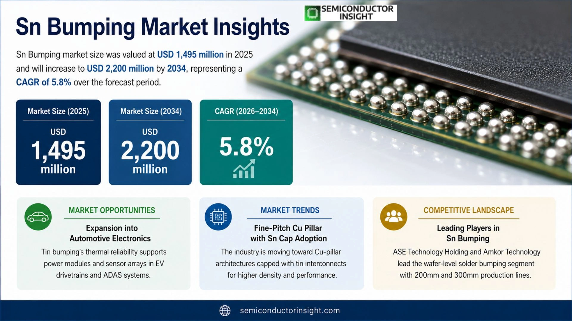
Sn Bumping market size was valued at USD 1,495 million in 2025 and will increase to USD 2,200 million by 2034, representing a CAGR of 5.8% over the forecast period.
Sn Bumping, also referred to as tin bumping, is an interconnect technique employed in semiconductor packaging where tin‑based solder bumps are created on wafer pads to enable flip‑chip bonding and wafer‑level chip‑scale packages (WLCSP). These bumps serve both electrical connections and mechanical support between the die and its substrate or interposer. Fabrication methods commonly include electroplating, stencil printing or ball placement followed by reflow, using pure tin or lead‑free alloys such as Sn‑Ag or Sn‑Ag‑Cu (SAC). Product variants span standard solder balls for flip‑chip/BGA applications, micro‑bumps for fine‑pitch WLCSP, and copper pillar caps for advanced three‑dimensional stacking.
MARKET DRIVERS
Rising Demand for Miniaturized Electronics
Sn Bumping market is gaining traction as smartphone manufacturers push for slimmer profiles and higher port counts. tin‑based micro‑bumps enable tighter pitch interconnects, which translates into more functionality per square millimetre of board real‑estate. This trend is especially pronounced in flagship devices where every millimetre of space is monetised.
Advances in Lead‑Free Soldering
Regulatory pressure to eliminate lead has accelerated investment in alternative processes, and tin bumping has emerged as the most mature lead‑free option. Improvements in flux chemistry and laser‑directed reflow have lifted defect rates to levels that rival traditional solder balls, making the technology attractive for high‑volume production lines.
➤ Industry surveys indicate that manufacturers adopting tin bumping report a 12‑15 % reduction in material cost per unit, while maintaining comparable reliability metrics.
From a strategic perspective, the cost advantage coupled with a greener footprint positions Sn Bumping market as a viable pathway for companies seeking to balance margin pressure with sustainability mandates.
MARKET CHALLENGES
Process Yield Variability
Although tin bumping offers clear benefits, achieving uniform bump height across large panels remains difficult. Minor variations in deposition thickness can trigger open‑circuit failures during subsequent assembly steps, prompting manufacturers to tighten process windows and increase inspection spend.
Other Challenges
Equipment Cost
State‑of‑the‑art bumping tools command premium prices, often exceeding the budget of small‑to‑mid‑size fabs. The high upfront investment can delay ROI, particularly when demand spikes are seasonal rather than sustained.
MARKET RESTRAINTS
Environmental Regulations on Lead‑Free Solder
Compliance with RoHS and equivalent standards imposes strict testing regimes on tin‑based interconnects. Companies must allocate resources to certify each new product, extending time‑to‑market and inflating overhead.
In parallel, the industry faces a shortage of engineers proficient in the nuances of tin bumping. Training programmes are still limited, forcing firms to compete for a narrow talent pool, which in turn drives wage pressures.
MARKET OPPORTUNITIES
Expansion into Automotive Electronics
The automotive sector’s shift toward electric drivetrains and advanced driver‑assistance systems demands reliable, high‑density connections. Tin bumping’s ability to withstand thermal cycling makes it a strong candidate for power modules and sensor arrays, opening a new revenue stream for suppliers.
Emergence of 3D‑Stacked Packages
3D integration requires inter‑die connections that are thinner than traditional solder balls. Tin bumping aligns with this requirement, and early adopters are already reporting improved signal integrity and reduced parasitic effects.
Service‑Based Business Models
Equipment manufacturers are introducing pay‑per‑use and performance‑based contracts that lower the barrier for entry. Such models enable smaller players to access cutting‑edge bumping technology without incurring full capital costs, thereby expanding the addressable market.
Sn Bumping Market Trends
Fine‑Pitch Cu Pillar with Sn Cap Adoption
The semiconductor packaging sector is witnessing a decisive move toward Cu‑pillar architectures capped with tin interconnects. As device footprints shrink and I/O counts climb, manufacturers gravitate to this combination because it delivers tighter control over joint geometry while preserving the mechanical compliance needed for thermal cycling. The transition is not merely a technical tweak; it reshapes equipment investment cycles, prompting fabs to retrofit electroplating lines for sub‑micron pillar formation and to qualify new reflow profiles that accommodate the higher melting point of copper. For suppliers, the shift translates into higher‑value tooling contracts and a longer sales horizon for ancillary consumables such as under‑bump metallization (UBM) chemistries. End‑users, meanwhile, gain access to package‑level performance that meets the bandwidth and power‑density expectations of emerging AI accelerators and high‑performance computing modules.
Other Trends
Lead‑Free Alloy Migration
Environmental regulations and customer specifications have accelerated the migration from traditional Sn‑Pb formulations to pure tin or tin‑silver‑copper alloys. Pure Sn offers lower reflow temperatures, which eases strain on temperature‑sensitive substrates, while Sn‑Ag‑Cu blends provide a favorable trade‑off between joint strength and electromigration resistance. The practical outcome is a reshuffling of inventory for material distributors and a push for process engineers to fine‑tune paste rheology to mitigate defect rates at ultra‑fine pitches. Companies that have already integrated inline metrology for alloy composition can differentiate themselves by guaranteeing batch‑to‑batch consistency, a factor that increasingly influences purchasing decisions.
Reliability Emphasis for 3D/Stacked Packages
As 3D interposers and high‑bandwidth memory (HBM) stacks become mainstream, the failure modes associated with Sn‑based bumps evolve. Electromigration at the Sn/Cu interface and the growth of intermetallic compounds (IMC) under prolonged current stress have emerged as critical reliability concerns. This reality has driven OEMs to co‑optimize UBM stack designs, bump geometry, and board‐level thermal management strategies. From a commercial perspective, the heightened focus on reliability opens opportunities for test service providers offering accelerated life‑cycle assessments, as well as for equipment vendors that can deliver high‑resolution inspection systems capable of detecting sub‑micron voids before they propagate. The net effect is a market that rewards firms able to provide end‑to‑end solutions,materials, processes, and validation,over those offering isolated products.
COMPETITIVE LANDSCAPE
Key Industry Players
Sn Bumping Competitive Landscape Overview
ASE Technology Holding and Amkor Technology dominate the wafer‑level solder bumping segment, each operating 200 mm and 300 mm lines that serve the high‑mix, high‑volume requirements of leading fabless designers. Their breadth of metallization options,electroplated, stencil‑printed, and ball‑placement,allows them to lock‑in customers seeking both cost‑effective standard BGA solutions and ultra‑fine micro‑bump architectures for 2.5 D/3D stacking. The depth of their R&D pipelines, particularly in Cu‑pillar‑with‑Sn‑cap processes, translates into tighter joint tolerances and lower electromigration risk, a decisive advantage as I/O densities surpass 200 µm pitch. Consequently, Tier‑1 fabs such as TSMC and Samsung routinely contract these OSATs for their most advanced nodes, reinforcing a market structure where scale, process flexibility, and reliability engineering become the primary barriers to entry.
Beyond the two giants, a diverse cohort of specialists occupies niche but strategically important positions. Companies like Powertech Technology, LB Semicon, and International Micro Industries focus on stencil‑printed and electroplated bumps for mid‑range applications, leveraging lower capital expenditure to attract regional customers in Asia‑Pacific. Meanwhile, pure‑play bumping providers such as Chipbond, ChipMOS, and Unisem Group have carved out reputations for rapid turn‑around on prototype runs, often collaborating with emerging AI‑chip designers that need customized alloy formulations (Sn‑Ag‑Cu, Sn‑Cu) to meet reliability targets. These players collectively sustain a competitive environment where differentiation rests on material expertise, localized service, and the ability to scale from pilot to volume without sacrificing defect control.
List of Key Sn Bumping Companies Profiled
- ASE Technology Holding
- Amkor Technology
- TSMC
- Samsung Electronics
- Powertech Technology Inc.
- LB Semicon Inc.
- International Micro Industries
- Chipbond
- ChipMOS Technologies
- Unisem Group
- Jiangsu CAS Microelectronics Integration
- SFA Semicon
- Shenzhen Tongxingda Technology
- FINECS
- Jiangsu Yidu Technology
Segment Analysis:
| Segment Category | Sub-Segments | Key Insights |
| By Type |
|
Micro Solder Bumps are emerging as the pivotal type for next‑generation packaging.
|
| By Application |
|
Flip‑Chip Packaging continues to dominate because it directly addresses performance and form‑factor pressures.
|
| By End User |
|
High‑Performance Computing is the leading end‑user segment, driving sophisticated bump solutions.
|
| By Wafer Size |
|
300 mm Wafer is the dominant format, offering scale advantages.
|
| By Material System |
|
Lead‑Free Sn‑Ag‑Cu has become the standard material system for reliability‑critical packages.
|
Regional Analysis: Sn Bumping Market
Asia‑Pacific
Taiwan’s foundry ecosystem clusters a majority of the copper‑to‑tin conversion processes, leveraging mature fabs and a seasoned workforce. The density of downstream packaging firms amplifies knowledge transfer, driving incremental refinements in bump geometry and alloy composition.
Regional trade agreements have insulated raw‑material flows, ensuring a steady tin feedstock supply despite geopolitical frictions. This stability allows manufacturers to lock in longer‑term contracts, reducing cost volatility for Sn Bumping market.
University‑industry consortia in South Korea and Singapore focus on nano‑scale bump adhesion, producing proprietary alloys that extend cycle life. Such breakthroughs are quickly commercialized, feeding a pipeline of differentiated offerings.
Local environmental standards encourage the shift away from lead, prompting early adoption of tin‑based solutions. Compliance requirements have become a catalyst for investment in Sn Bumping equipment across the region.
North America
While North America lags behind in sheer volume, its market is shaped by high‑value, low‑volume applications such as aerospace and defense. OEMs prioritize reliability over cost, driving demand for premium tin alloys with tighter defect thresholds. The presence of leading equipment manufacturers in the United States creates a robust service infrastructure, but recurring supply‑chain constraints for tin concentrate on the need for strategic stockpiles. Regulatory pressure to eliminate lead in consumer electronics adds momentum, yet the region’s adoption curve is moderated by the longer product development cycles typical of its targeted sectors.
Europe
European firms approach Sn Bumping from a compliance‑first perspective, aligning with stringent EU directives on hazardous substances. This regulatory rigor spurs early experimentation with lead‑free bumping processes, especially in automotive electronics where safety certifications are paramount. Regional clusters in Germany and the Netherlands combine precision engineering with an emphasis on circular‑economy principles, encouraging recycling of tin waste. Market participants therefore invest in equipment capable of handling recycled feedstock without compromising bump integrity, positioning Europe as a testbed for sustainable practices.
South America
South America’s involvement is driven primarily by emerging consumer‑electronics assembly plants in Brazil and Mexico. Cost considerations dominate, prompting manufacturers to evaluate tin‑based bumping as a means to reduce material expenses while meeting baseline reliability standards. Nevertheless, the region faces logistical hurdles, including limited domestic tin processing capacity and dependence on imports. Companies that succeed tend to partner with global distributors to secure reliable supply lines, turning the market into a niche arena for value‑oriented solutions rather than cutting‑edge alloy development.
Middle East & Africa
In the Middle East & Africa, Sn Bumping market is still nascent, with activity centered around pilot projects in smart‑city infrastructure and telecom rollout. Government initiatives to diversify economies beyond oil and minerals have encouraged modest investment in semiconductor packaging. However, a shortage of skilled technicians and the absence of a dedicated supply chain for tin alloys constrain scaling. Early adopters focus on training programs and joint ventures with Asian partners to import expertise, laying groundwork for a gradual expansion of the market footprint.
Report Scope
This market research report provides a comprehensive analysis of the Sn Bumping Market , covering the forecast period 2026–2034. It offers detailed insights into market dynamics, technological advancements, competitive landscape, and key trends shaping the industry.
Key focus areas of the report include:
- Market Overview: The report begins with an overview outlining its current market scenario, key growth indicators, and industry transformation drivers. It discusses macroeconomic factors, demand–supply balance, regulatory landscape, and the strategic role of semiconductors in powering advancements across industries such as automotive, telecommunications, consumer electronics, and industrial automation.
- Market Size & Forecast: Historical data and future projections for revenue, unit shipments, and market value across major regions and segments.
- Segmentation Analysis: Detailed breakdown by product type, technology, application, and end-user industry to identify high-growth segments and investment opportunities.
- Regional Insights: Insights into market performance across North America, Europe, Asia-Pacific, Latin America, and the Middle East & Africa, including country-level analysis where relevant.
- Competitive Landscape: Profiles of leading market participants, including their product offerings, R&D focus, manufacturing capacity, pricing strategies, and recent developments such as mergers, acquisitions, and partnerships.
- Technology Trends & Innovation: Assessment of emerging technologies, integration of AI/IoT, semiconductor design trends, fabrication techniques, and evolving industry standards.
- Market Drivers & Restraints: Evaluation of factors driving market growth along with challenges, supply chain constraints, regulatory issues, and market-entry barriers.
- Stakeholder Insights: Insights for component suppliers, OEMs, system integrators, investors, and policymakers regarding the evolving ecosystem and strategic opportunities.
Primary and secondary research methods are employed, including interviews with industry experts, data from verified sources, and real-time market intelligence to ensure the accuracy and reliability of the insights presented.
FREQUENTLY ASKED QUESTIONS:
What is the current market size of Sn Bumping Market?
-> Sn Bumping market size was valued at USD 1,495 million in 2025 and will increase to USD 2,200 million by 2034, representing a CAGR of 5.8%
Which key companies operate in Sn Bumping Market?
-> Key players include ASE, Amkor Technology, TSMC, Samsung, Intel, Powertech Technology Inc., LB Semicon Inc., and other leading OSATs and advanced‑packaging firms.
What are the key growth drivers?
-> Key growth drivers include finer pitch and higher I/O density accelerating Cu‑pillar + Sn‑cap adoption, mainstreaming of lead‑free solder alloys (Sn‑Ag, Sn‑Cu, SAC), and rising reliability constraints in advanced 3D/stacked packages requiring co‑optimization of materials and UBM.
Which region dominates the market?
-> Asia-Pacific dominates Sn Bumping market, driven by strong demand and extensive OSAT capacity in China, Japan, and South Korea, while North America and Europe also show significant activity.
What are the emerging trends?
-> Emerging trends include integration of Sn caps on Cu pillars for tighter joint control, micro‑bump interconnects for 2.5D/3D HBM packages, and continued development of advanced lead‑free alloy compositions to meet stringent reliability standards.

Get Sample Report PDF for Exclusive Insights
Report Sample Includes
- Table of Contents
- List of Tables & Figures
- Charts, Research Methodology, and more...
 Download Sample Report PDF