Gold Bumped Wafer Market Insights
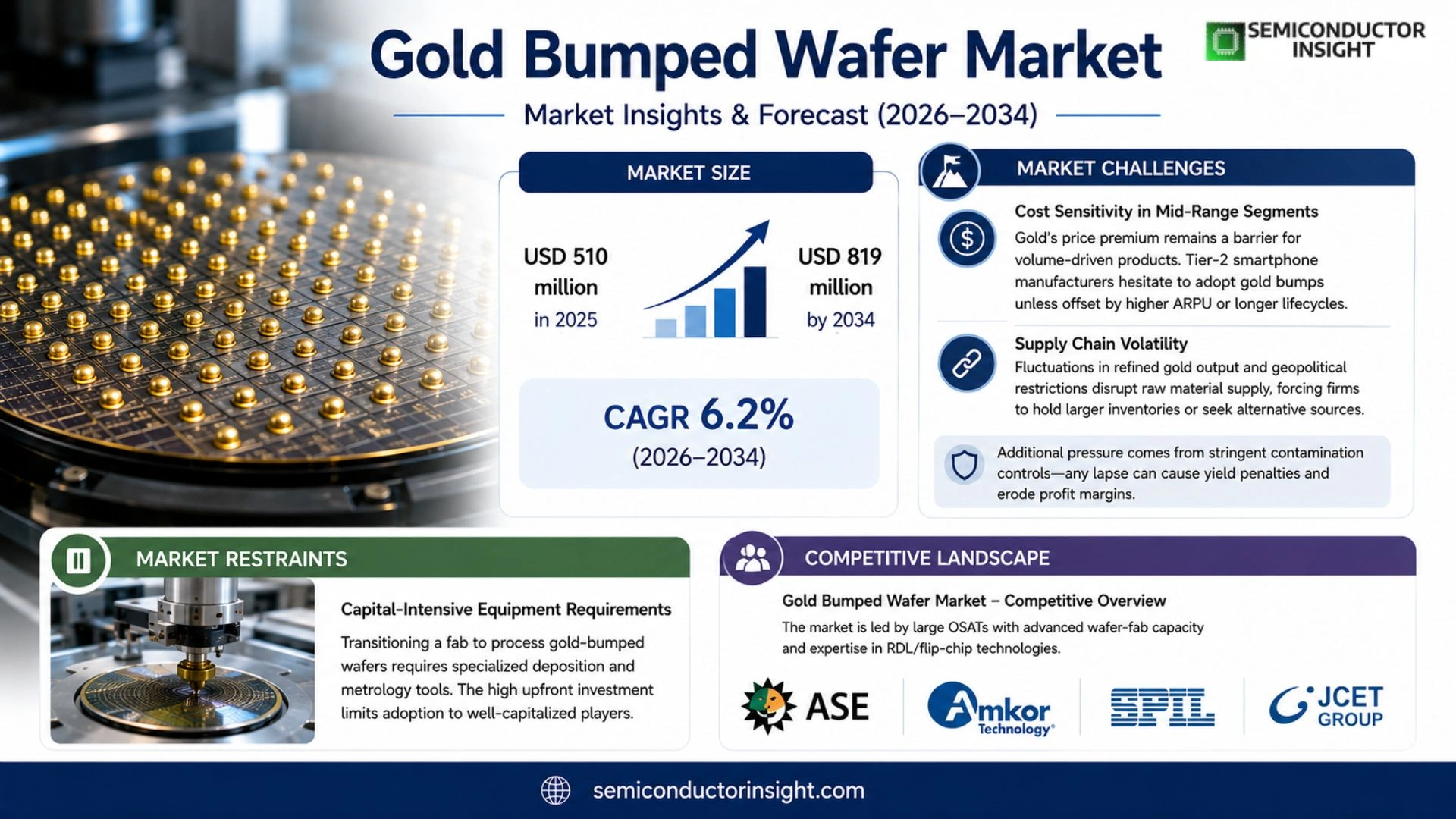
Gold Bumped Wafer market size was valued at USD 510 million in 2025 and will increase to USD 819 million by 2034, exhibiting a CAGR of 6.2% over the forecast period.
Gold Bumped Wafer refers to a wafer‑level finished form where Au bumps are created on die pads to enable high‑density first‑level interconnect for flip‑chip or tape/glass/film assembly flows. Two main routes dominate the product family: (1) Au stud/ball bumps derived from thermosonic wire‑bond ball bonding, where the wire is terminated after the initial bond leaving a bump; and (2) electroplated Au bumps produced via thin‑film/UBM, photolithography opening and electroplating, allowing parallel bump formation across the wafer.
Growth stems from rising demand for fine‑pitch, low‑profile interconnects in display‑driver ecosystems such as COF/COG, where gold bumps support ultra‑thin, high‑pin‑count requirements. Cost pressure on Au prices also encourages adoption of composite metal stacks that retain reliability while lowering material usage.
MARKET DRIVERS
Advanced Packaging Demand
The surge in high‑density interconnect requirements is compelling semiconductor manufacturers to adopt finer pitch solutions. Gold Bumped Wafer Market benefits because the material’s conductivity and reliability align perfectly with these specifications, prompting design teams to favor gold bumps over traditional copper in premium segments.
Shift Toward Miniaturized Devices
Consumer electronics and edge‑AI modules are converging on sub‑millimeter form factors. This trend forces suppliers to deliver wafers that can sustain performance despite reduced die size. Gold’s resistance to corrosion and its stable electromigration profile make it a logical choice, driving procurement volumes across multiple fab lines.
➤ Manufacturers report a noticeable uptick in gold‑bumped wafer orders as they target gateways for 5G and automotive safety systems.
In parallel, the premium‑device segment is allocating a larger share of its R&D budget to materials that guarantee yield stability. The strategic emphasis on gold bumps translates into a steady pipeline of contracts for specialty foundries, reinforcing the market’s upward trajectory.
MARKET CHALLENGES
Cost Sensitivity in Mid‑Range Segments
While gold offers unmatched performance, its price premium remains a barrier for volume‑driven products. Tier‑2 smartphone manufacturers express reluctance to embed gold bumps unless the cost differential can be offset by higher ARPU or extended product lifecycles.
Other Challenges
Supply Chain Volatility
Fluctuations in refined gold output, combined with geopolitical trade restrictions, occasionally disrupt the steady flow of raw material to wafer fabs, forcing firms to hold larger inventories or seek alternative sourcing strategies.
Additional pressure stems from the need to maintain stringent contamination controls. Any lapse in cleanroom protocols can nullify gold’s advantages, leading to yield penalties that erode profit margins.
MARKET RESTRAINTS
Capital‑Intensive Equipment Requirements
Transitioning a fab to handle gold‑bumped wafers demands specialized deposition tools and metrology suites. The upfront investment often exceeds the budget thresholds of smaller foundries, limiting market participation to well‑capitalized players.
The learning curve associated with process qualification further extends time‑to‑market, discouraging firms that operate on tight product launch windows. As a result, adoption rates plateau in regions where financing constraints are pronounced.
Regulatory scrutiny over precious‑metal usage also imposes documentation burdens, especially in jurisdictions with stringent reporting on metal traceability. Compliance costs add another layer of restraint for companies evaluating expansion into the gold‑bump niche.
MARKET OPPORTUNITIES
Emerging 3D‑IC Architectures
Three‑dimensional integration strategies are unlocking new design space for high‑performance computing. Gold’s superior bonding characteristics make it ideal for vertical interconnects, positioning Gold Bumped Wafer market as a foundational supplier for next‑generation 3D‑IC stacks.
Parallel advances in additive manufacturing of metal interconnects present a collaborative avenue. Joint ventures between wafer fabs and metal‑printing specialists could lower incremental costs, widening the addressable market beyond traditional high‑value segments.
Finally, strategic partnerships with automotive OEMs developing autonomous driving platforms open a sizeable, long‑term revenue stream. The stringent reliability standards of safety‑critical systems align with gold’s proven track record, encouraging co‑development agreements that embed gold bumps from silicon onward.
Gold Bumped Wafer Market Trends
Shift Toward Fine‑Pitch Gold Bumps
The display‑driver ecosystem is tightening its geometry as panel resolutions climb and bezel dimensions shrink. Engineers respond by reducing gold bump diameter and spacing, moving from standard 50 µm pitch to sub‑25 µm configurations. This refinement improves signal integrity for COF/COG assemblies while preserving the low‑profile advantage of Au‑based interconnects. Suppliers such as ChipMOS have expanded 12‑inch capacity to accommodate finer layouts, recognizing that tighter pitch directly influences yield in ultra‑thin glass or flexible OLED modules. Consequently, design houses are allocating more silicon real‑estate to Au‑bumped regions, reshaping the wafer‑level layout hierarchy.
Other Trends
Cost Management Amidst Gold Price Volatility
Fluctuations in precious‑metal markets pressure manufacturers to trim Au consumption without sacrificing reliability. A noticeable response is the incorporation of Cu/Ni/Au composite stacks, where a thin gold capping layer protects underlying copper while delivering comparable bonding performance. This approach aligns with thermocompression processes that tolerate modest alloy variations. Large OSATs are piloting mixed‑metal bump lines, allowing customers to select a cost‑effective alloy based on volume and performance criteria. The shift reduces material expense and mitigates supply‑chain exposure, albeit at the cost of added process complexity in UBM engineering.
Platform Bifurcation and Niche Applications
While Cu‑pillar micro‑bumps dominate leading‑edge flip‑chip solutions, gold‑bumped wafers retain relevance in segments where low profile, high uniformity, and ACF‑compatible bonding are non‑negotiable. Sensors for automotive radar, RF front‑ends, and harsh‑environment modules continue to rely on Au‑Au thermosonic or thermocompression joins because of proven thermal stability. The bifurcated platform landscape forces vendors to maintain parallel capability sets: high‑volume Cu‑centric lines for mainstream logic and dedicated gold‑bump streams for display drivers, sensor arrays, and specialized packaging formats. This dual track influences capacity planning, workforce skill sets, and capital allocation across Gold Bumped Wafer market.
COMPETITIVE LANDSCAPE
Key Industry Players
Gold Bumped Wafer Market – Competitive Overview
Gold‑bumped wafer segment is anchored by a handful of large‑scale OSATs that possess the wafer‑fab capacity and advanced RDL/flip‑chip expertise required to service high‑volume display‑driver customers. ASE Technology Holding and Amkor Technology dominate this tier, each operating 12‑inch lines capable of both thermosonic stud‑ball and electroplated Au processes. Their breadth of service,from UBM metallization through to final ACF integration,makes them the default suppliers for major LCD/OLED panel makers seeking consistent yield and tight pitch control. Both firms have leveraged their global footprint to offer localized engineering support, thereby reducing time‑to‑qualification for new COF/COG designs. The result is a concentration of market share that forces smaller entrants to specialize or partner in order to access the same customer base.
Beyond the two giants, a diverse cohort of niche players sustains the ecosystem with depth in specific technologies or regional markets. ChipMOS Technologies and Chipbond Technology Corporation have carved out leadership in fine‑pitch electroplated Au bumps for ultra‑thin COF applications, often bundling proprietary grinding and singulation steps that meet aggressive bezel requirements. Companies such as Steco, LB Semicon Inc, and Nepes focus on composite‑metal stacks that mitigate gold price volatility while preserving bonding integrity. Regional specialists,including Hefei Chipmore Technology, Union Semiconductor (Hefei) Co., Ltd., Shenzhen TXD Technology, Jiangsu Yidu Technology, Tongfu Microelectronics (TFME) and China Wafer Level CSP Co., Ltd,provide tailored services to domestic display manufacturers, capitalizing on shorter supply chains and localized know‑how. Their collective presence ensures that even low‑volume or highly customized projects can secure a qualified gold‑bumped wafer source.
List of Key Gold Bumped Wafer Companies Profiled
- ASE Technology Holding
- Amkor Technology
- ChipMOS Technologies
- Chipbond Technology Corporation
- Steco
- LB Semicon Inc
- Nepes
- Hefei Chipmore Technology
- Union Semiconductor (Hefei) Co., Ltd.
- Shenzhen TXD Technology
- Jiangsu Yidu Technology
- Tongfu Microelectronics (TFME)
- China Wafer Level CSP Co., Ltd
Segment Analysis:
| Segment Category | Sub-Segments | Key Insights |
| By Type |
|
Electroplated Au Bumps – Enables wafer‑level parallel bump formation with tight pitch control. – Preferred for high‑pin‑count display driver packages where uniformity and low profile are critical. – Aligns with advanced lithographic processes, supporting fine‑pitch migration and cost‑effective scaling. |
| By Application |
|
Display Driver (COF/COG) – Drives the strongest pull due to ultra‑thin, high‑pin‑count interconnect needs. – Supports fine‑pitch COF migration and narrow‑bezel OLED panels. – Benefits from Au’s superior adhesion and compatibility with anisotropic conductive films. |
| By End User |
|
Smartphones & Tablets – Prioritize ultra‑fine pitch for high‑resolution panels. – Require reliable Au‑Au bonding for thin‑glass or flexible substrates. – Favor process routes that minimize Au usage while preserving performance. |
| By Technology |
|
Fine Pitch – Addresses the shift toward higher pixel densities and narrow‑bezel designs. – Enables staggered bump layouts that improve mechanical stability. – Drives innovation in lithography and electroplating precision. |
| By Process |
|
Photolithography & Electroplating – Provides superior control over bump geometry and uniformity. – Supports integration with UBM layers that enhance adhesion and diffusion barrier performance. – Aligns with wafer‑scale production for cost‑effective high‑volume output. |
Regional Analysis: Gold Bumped Wafer Market
Europe
Leading fabs in the Benelux and central Europe have retrofitted existing 200 mm lines with gold‑bump deposition modules, reducing capital outlay while preserving throughput. This incremental upgrade path attracts mid‑size players seeking competitive differentiation without a full‑scale greenfield investment.
The regional concentration of gold refineries near the Mediterranean ensures a stable metal feedstock. Concurrently, logistics firms have built dedicated cold‑chain routes for wafer transport, limiting contamination risk and preserving yield.
EU directives on critical materials favor responsible sourcing, prompting manufacturers to document provenance for every gram of gold used. Compliance frameworks have become a market entry prerequisite for non‑EU suppliers.
Automotive OEMs in Germany and Sweden are specifying gold‑bumped wafers for next‑generation ADAS modules, valuing the technology’s thermal stability and low contact resistance in harsh environments.
North America
The United States remains a formidable demand source, driven by defense contracts that require ultra‑reliable interconnects. However, fabs often rely on European equipment vendors for gold‑bump tooling, creating a cross‑regional dependency that influences pricing negotiations and technology road‑maps.
Asia‑Pacific
East Asian manufacturers are accelerating pilot programs to integrate gold bumps into high‑volume smartphone chips. While cost considerations dominate, the region’s growing emphasis on reliability for foldable displays nudges a segment of producers toward premium‑grade solutions despite higher material expenses.
South America
Brazil’s emerging semiconductor cluster views gold‑bumped wafers as a niche differentiator for aerospace applications. Limited local refining capacity forces import reliance, which in turn shapes partnership strategies with European suppliers seeking market diversification.
Middle East & Africa
The Gulf Cooperation Council’s investment in smart‑city infrastructure has sparked interest in gold‑bumped technologies for sensor networks. Local foundries are still nascent, so most of the value chain is sourced externally, making geopolitical stability a key factor for long‑term planning.
Report Scope
This market research report provides a comprehensive analysis of the Gold Bumped Wafer Market , covering the forecast period 2026–2034. It offers detailed insights into market dynamics, technological advancements, competitive landscape, and key trends shaping the industry.
Key focus areas of the report include:
- Market Overview: The report begins with an overview outlining its current market scenario, key growth indicators, and industry transformation drivers. It discusses macroeconomic factors, demand–supply balance, regulatory landscape, and the strategic role of semiconductors in powering advancements across industries such as automotive, telecommunications, consumer electronics, and industrial automation.
- Market Size & Forecast: Historical data and future projections for revenue, unit shipments, and market value across major regions and segments.
- Segmentation Analysis: Detailed breakdown by product type, technology, application, and end-user industry to identify high-growth segments and investment opportunities.
- Regional Insights: Insights into market performance across North America, Europe, Asia-Pacific, Latin America, and the Middle East & Africa, including country-level analysis where relevant.
- Competitive Landscape: Profiles of leading market participants, including their product offerings, R&D focus, manufacturing capacity, pricing strategies, and recent developments such as mergers, acquisitions, and partnerships.
- Technology Trends & Innovation: Assessment of emerging technologies, integration of AI/IoT, semiconductor design trends, fabrication techniques, and evolving industry standards.
- Market Drivers & Restraints: Evaluation of factors driving market growth along with challenges, supply chain constraints, regulatory issues, and market-entry barriers.
- Stakeholder Insights: Insights for component suppliers, OEMs, system integrators, investors, and policymakers regarding the evolving ecosystem and strategic opportunities.
Primary and secondary research methods are employed, including interviews with industry experts, data from verified sources, and real-time market intelligence to ensure the accuracy and reliability of the insights presented.
FREQUENTLY ASKED QUESTIONS:
What is the current market size of Gold Bumped Wafer Market?
-> Gold Bumped Wafer market size will increase to USD 819 million by 2034, exhibiting a CAGR of 6.2% over the forecast period.
Which key companies operate in Gold Bumped Wafer Market?
-> Key players include Nepes, LB Semicon Inc, ChipMOS TECHNOLOGIES, Chipbond Technology Corporation, Steco, Hefei Chipmore Technology, Union Semiconductor (Hefei) Co., Ltd., Shenzhen TXD Technology, Jiangsu Yidu Technology, Tongfu Microelectronics (TFME), China Wafer Level CSP Co., Ltd.
What are the key growth drivers?
-> Key growth drivers include finer pitch and higher pin‑density demand driven by high‑resolution and OLED panels, cost pressure and Au price volatility prompting metal‑composite bump adoption, and platform bifurcation where Cu pillar dominates leading‑edge flip‑chip while Au bumping remains essential for display‑driver and sensor applications.
Which region dominates the market?
-> Asia‑Pacific is the dominant region, driven by a large concentration of OSATs, display‑driver manufacturers and growing demand for advanced interconnect solutions.
What are the emerging trends?
-> Emerging trends include adoption of Cu/Ni/Au composite bumps to reduce gold usage, migration to 12‑inch fine‑pitch COF platforms, and integration of ultra‑fine pitch (<25 µm) technologies for high‑density sensor and RF modules.

Get Sample Report PDF for Exclusive Insights
Report Sample Includes
- Table of Contents
- List of Tables & Figures
- Charts, Research Methodology, and more...
 Download Sample Report PDF