Multilayer Ceramic Packages Market Insights
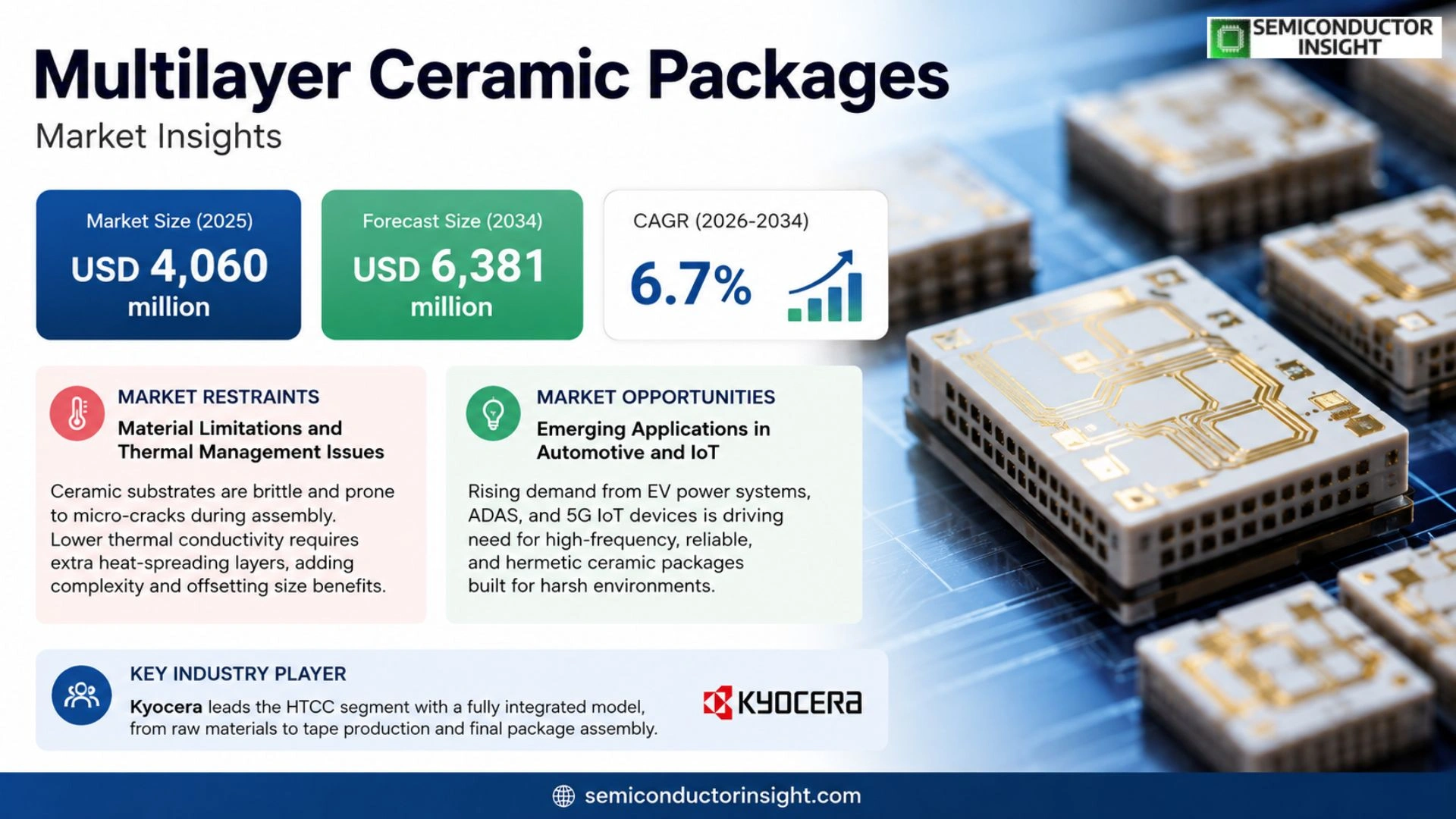
Multilayer Ceramic Packages market was valued at USD 4,060 million in 2025 and is projected to reach USD 6,381 million by 2034, exhibiting a CAGR of 6.7 % during the forecast period.
Multilayer Ceramic Packages are co‑fired, tape‑based ceramic substrate platforms built by stacking multiple “green” ceramic tapes that embed conductors and vias. After lamination the stack is sintered into a monolithic body, providing high structural robustness, low thermal‑expansion mismatch and true three‑dimensional routing with cavity structures. The typical flow includes tape forming, via/cavity creation and filling, thick‑film conductor printing, lamination and co‑firing; low‑temperature LTCC operates around 850–900 °C whereas high‑temperature HTCC requires approximately 1{600} °C.
MARKET DRIVERS
Rising Demand for High‑Performance Miniaturized Electronics
Multilayer Ceramic Packages Market is being pulled forward by a wave of compact devices that require superior frequency handling and thermal stability. Mobile handsets, wearables, and edge‑compute modules now embed more functionality per square millimeter, compelling OEMs to seek packaging solutions that can sustain higher signal integrity without enlarging the footprint. This shift directly translates into higher bill‑of‑materials spend on multilayer ceramic substrates, as designers prioritize reliability over marginal cost savings.
Accelerating Adoption of Advanced Packaging Technologies
Industries such as aerospace, defense, and automotive are incorporating system‑in‑package (SiP) architectures that layer passive and active components within a single ceramic stack. The ability to integrate passives, antennas, and power modules in a thin, hermetic package reduces assembly steps and improves overall product yield. Consequently, suppliers that can offer fine‑line printing and laser‑drilled interconnects see a measurable uplift in order volume.
➤ Analysts note that the average unit price for a 6‑layer ceramic package has risen by roughly 12 % over the past 24 months, reflecting both heightened demand and incremental value‑added services.
From a strategic perspective, the trend forces traditional silicon‑based packagers to either diversify into ceramic solutions or risk losing market share to niche players that already possess the required expertise and equipment. Companies that secure early access to emerging materials,such as low‑k dielectric ceramics,stand to capture a disproportionate share of the upside.
MARKET CHALLENGES
Cost Pressures From Complex Manufacturing
Fabricating a multilayer ceramic stack involves multiple high‑temperature sintering cycles, precision laser drilling, and meticulous metallization. Each step adds labor and equipment depreciation costs, making the final package significantly pricier than conventional organic substrates. When tier‑1 manufacturers negotiate price points, they often push suppliers to trim margins, which can erode investment in R&D for next‑generation processes.
Other Challenges
Supply Chain Volatility
The reliance on specialty powders, high‑purity alumina, and scarce rare‑earth dopants introduces material‑sourcing bottlenecks. Recent geopolitical tensions have amplified lead times for key inputs, compelling fabs to hold higher inventory levels,a practice that inflates working capital and compresses cash flow.
MARKET RESTRAINTS
Material Limitations and Thermal Management Issues
Despite their electrical advantages, ceramic substrates suffer from inherent brittleness, which restricts wafer‑scale handling and raises the risk of micro‑cracks during high‑speed assembly. Moreover, as device power densities climb, the low thermal conductivity of certain ceramic formulations becomes a bottleneck, forcing designers to embed additional heat‑spreading layers that offset some of the size benefits originally sought.
MARKET OPPORTUNITIES
Emerging Applications in Automotive and IoT
Electric‑vehicle power‑train controllers and advanced driver‑assistance systems (ADAS) increasingly depend on resilient, high‑frequency interconnects that can survive harsh temperature cycles. Multilayer ceramic packages meet these criteria, opening a lucrative avenue for vendors willing to certify their products to automotive-grade standards. Simultaneously, the proliferation of 5G‑enabled IoT nodes,many of which operate in remote or industrial settings,creates a demand for hermetic, low‑loss packaging that can maintain performance over extended lifespans.
Multilayer Ceramic Packages Market Trends
Thermal Reliability as a Differentiator
The HTCC segment continues to attract aerospace and medical device manufacturers because its ability to withstand temperatures above 1,500 °C aligns with the stringent durability requirements of these sectors. Hermetic sealing and low coefficient of thermal expansion enable long‑life enclosures for implantable sensors and defense‑grade avionics, where any dimensional drift can compromise performance. Suppliers are incorporating alumina‑rich glass‑ceramic formulations that reduce micro‑cracking during thermal cycling, thereby extending lifecycle predictions for critical hardware. This focus on structural integrity is reshaping supplier investments, prompting a wave of equipment upgrades that prioritize tighter tolerance control and enhanced sintering uniformity.
Other Trends
RF Integration in Automotive Electronics
LTCC’s low dielectric loss and ability to embed inductors and capacitors within the ceramic stack are making it the preferred substrate for vehicle‑to‑infrastructure transceivers and advanced driver‑assistance radar modules. Automakers are consolidating RF front‑ends onto a single multilayer board to cut interconnect count and improve signal integrity at 5 GHz and above. The migration from discrete components to monolithic, three‑dimensional structures reduces assembly steps and aligns with the industry’s push for lighter, more compact powertrain electronics. As a result, design houses are revising reference architectures to exploit LTCC’s fine line capability and inherent shielding characteristics.
Shift Toward Embedded Passives
Across consumer and communications segments, the drive to minimize bill‑of‑materials cost is steering engineers toward packages that combine routing, cavity formation, and passive functionality in one monolithic component. Recent material advances, such as low‑tan glass‑ceramics and improved CTE‑matched laminates, are enabling tighter layer alignment and higher density via arrays. These technical gains translate into fewer substrate changes during product development and a smoother qualification pathway for high‑frequency modules. Companies that can offer modular design kits featuring pre‑engineered passive patterns are positioning themselves as strategic partners for OEMs seeking rapid time‑to‑market for next‑generation wireless devices.
COMPETITIVE LANDSCAPE
Key Industry Players
Multilayer Ceramic Packages: Competitive Overview
Kyocera dominates the high‑temperature ceramic (HTCC) segment through a tightly integrated supply chain that spans raw material sourcing, tape fabrication, and final package assembly. Its portfolio commands a premium in defense, aerospace, and medical implants where hermeticity and mechanical strength dictate selection criteria. By leveraging a global production footprint and a robust engineering services arm, Kyocera has locked in long‑term contracts with major OEMs, creating a market structure where a handful of vertically‑strong firms capture the bulk of high‑reliability revenue while allocating space for specialist LTCC providers that focus on frequency‑sensitive applications.
Beyond the tier‑1 leaders, a cluster of niche players extends the ecosystem’s depth. Murata and TDK have concentrated on low‑temperature LTCC solutions that embed passive functions, enabling compact RF front‑ends for automotive and 5G communications. Samsung Electro‑Mechanics pursues high‑volume automotive modules, emphasizing dimensional stability and cost efficiency. Smaller Chinese manufacturers such as Jiangsu Yixing Electronics, Chaozhou Three‑Circle Group, Hebei Sinopack Electronic Technology, and CETC 43 (Shengda Electronics) differentiate through rapid design turn‑around and customized cavity‑type packages for industrial IoT devices. Their collective focus on process optimisation and material innovation sustains a competitive pressure that forces the larger incumbents to refine pricing and broaden application coverage.
List of Key Multilayer Ceramic Packages Companies Profiled
- Kyocera
- Murata Manufacturing
- TDK Corporation
- Samsung Electro‑Mechanics
- Ametek Aegis
- Electronic Products, Inc. (EPI)
- Jiangsu Yixing Electronics
- Chaozhou Three‑Circle Group
- Hebei Sinopack Electronic Technology
- CETC 43 (Shengda Electronics)
- Mini‑Circuits
- Yokowo
- Walsin Technology
- Shenzhen Sunlord Electronics
- Microgate
Segment Analysis:
| Segment Category | Sub-Segments | Key Insights |
| By Type |
|
HTCC Ceramic Package is considered the leading segment for applications where hermeticity, mechanical strength, and high‑temperature operation are paramount.
|
| By Application |
|
Communications drives the most dynamic demand for multilayer ceramic packages due to the need for high‑frequency, low‑loss interconnects.
|
| By End User |
|
Device Manufacturers constitute the leading end‑user group as they directly embed LTCC and HTCC solutions into next‑generation electronic products.
|
| By Material |
|
Alumina Multilayer Substrates remain the dominant material choice because of their proven mechanical robustness and thermal conductivity.
|
| By Functional Integration |
|
Embedded Passive Packages are emerging as the most strategic segment, enabling multifunctional modules that combine interconnects, inductors, capacitors and resistors within a single ceramic body.
|
Regional Analysis: Multilayer Ceramic Packages Market
Asia‑Pacific
Capacity expansions across China, Taiwan, and South Korea have lifted wafer throughput by double‑digit percentages, allowing customers to secure larger volumes without compromising lead‑times. Facilities are increasingly modular, supporting rapid scale‑up for niche high‑frequency products while preserving cost efficiency for mass‑market items.
Recent disruptions have prompted firms to diversify upstream raw‑material sources, integrating locally sourced alumina and specialty powders. This shift reduces exposure to geopolitical shocks and shortens the logistics loop, translating into more predictable procurement for end‑users.
R&D consortia backed by national agencies focus on ultra‑thin dielectric layers and high‑k materials, targeting performance thresholds required for next‑generation AI accelerators. Collaborative patents have risen, signalling a move from isolated R&D toward shared technology roadmaps.
Harmonized standards across the region streamline certification for automotive and medical devices, enabling quicker market entry. Regulators are also emphasizing environmental compliance, encouraging the adoption of lead‑free sintering processes.
North America
North America retains a strong design‑leadership role, with major semiconductor houses orchestrating system‑level integration for premium applications. While manufacturing volumes are modest compared to Asia‑Pacific, the region’s focus on reliability and security drives demand for high‑performance ceramic packages in defense and aerospace. Partnerships between universities and corporate labs accelerate the exploration of novel substrate compositions, ensuring that the market remains receptive to cutting‑edge specifications even as cost pressures intensify.
Europe
European players leverage a disciplined engineering culture, emphasizing stringent quality controls and compliance with EU environmental directives. Automotive manufacturers, especially in Germany and France, demand ceramic solutions that can survive extreme thermal cycles, prompting local suppliers to refine their fire‑retardant formulations. The continent’s emphasis on sustainability also fuels interest in recyclable packaging designs, aligning product development with broader corporate ESG mandates.
South America
In South America, growth is anchored by expanding telecommunications infrastructure and a nascent electric‑vehicle sector. Local assemblers are beginning to replace traditional leaded packages with ceramic alternatives to meet emerging emission standards. Although the market remains fragmented, regional trade agreements are reducing tariff barriers, encouraging cross‑border component sourcing and fostering a modest yet noticeable uplift in demand.
Middle East & Africa
The Middle East & Africa region exhibits a cautious but steady adoption trajectory, propelled by investments in data‑center capacity and renewable‑energy projects. Operators prioritize durability and thermal stability, qualities inherent to multilayer ceramic packages, especially for desert‑climate deployments. Emerging partnerships between Gulf‑based electronics firms and Asian manufacturers are facilitating technology transfer, gradually building local expertise and expanding the market footprint.
Report Scope
This market research report provides a comprehensive analysis of the Multilayer Ceramic Packages Market , covering the forecast period 2026–2034. It offers detailed insights into market dynamics, technological advancements, competitive landscape, and key trends shaping the industry.
Key focus areas of the report include:
- Market Overview: The report begins with an overview outlining its current market scenario, key growth indicators, and industry transformation drivers. It discusses macroeconomic factors, demand–supply balance, regulatory landscape, and the strategic role of semiconductors in powering advancements across industries such as automotive, telecommunications, consumer electronics, and industrial automation.
- Market Size & Forecast: Historical data and future projections for revenue, unit shipments, and market value across major regions and segments.
- Segmentation Analysis: Detailed breakdown by product type, technology, application, and end-user industry to identify high-growth segments and investment opportunities.
- Regional Insights: Insights into market performance across North America, Europe, Asia-Pacific, Latin America, and the Middle East & Africa, including country-level analysis where relevant.
- Competitive Landscape: Profiles of leading market participants, including their product offerings, R&D focus, manufacturing capacity, pricing strategies, and recent developments such as mergers, acquisitions, and partnerships.
- Technology Trends & Innovation: Assessment of emerging technologies, integration of AI/IoT, semiconductor design trends, fabrication techniques, and evolving industry standards.
- Market Drivers & Restraints: Evaluation of factors driving market growth along with challenges, supply chain constraints, regulatory issues, and market-entry barriers.
- Stakeholder Insights: Insights for component suppliers, OEMs, system integrators, investors, and policymakers regarding the evolving ecosystem and strategic opportunities.
Primary and secondary research methods are employed, including interviews with industry experts, data from verified sources, and real-time market intelligence to ensure the accuracy and reliability of the insights presented.
FREQUENTLY ASKED QUESTIONS:
What is the current market size of Multilayer Ceramic Packages Market?
-> Multilayer Ceramic Packages market is projected to reach USD 6,381 million by 2034, exhibiting a CAGR of 6.7 % during the forecast period.
Which key companies operate in Multilayer Ceramic Packages Market?
-> Key players include Kyocera, Maruwa, NGK/NTK, Egide, NEO Tech, AdTech Ceramics, AMETEK Aegis, Electronic Products, Inc. (EPI), SoarTech, CETC 43 (Shengda Electronics), Jiangsu Yixing Electronics, Chaozhou Three-Circle (Group), Hebei Sinopack Electronic Tech & CETC 13, Beijing BDStar Navigation (Glead), Fujian Minhang Electronics, RF Materials (METALLIFE), CETC 55, Qingdao Kerry Electronics, Hebei Dingci Electronic, Murata Manufacturing, TDK Corporation, Mini-Circuits, Taiyo Yuden, Samsung Electro-Mechanics, Yokowo, ACX Corp, Yageo (Chilisin), Walsin Technology, Shenzhen Sunlord Electronics, Microgate.
What are the key growth drivers?
-> Key growth drivers include rising RF and mmWave complexity, automotive electronics reliability and integration, long‑life hermetic protection for medical and industrial applications, migration toward interconnects with embedded passives and 3D cavities, and ongoing material and process upgrades such as low‑tan LTCC and improved CTE‑matching.
Which region dominates the market?
-> Asia‑Pacific leads the market, while Europe remains a significant region.
What are the emerging trends?
-> Emerging trends include advanced LTCC integration for automotive control modules, RF/microwave and Si‑photonics interconnects, high‑frequency optical communication substrates, and enhanced low‑warpage, low‑CTE ceramic materials.

Get Sample Report PDF for Exclusive Insights
Report Sample Includes
- Table of Contents
- List of Tables & Figures
- Charts, Research Methodology, and more...
 Download Sample Report PDF