Key Statistics
Key Takeaways
- 200 mm SiC ion implanters are the fastest-growing equipment type because major power-semiconductor manufacturers are moving from 150 mm to 200 mm wafers to improve die output and manufacturing economics. Wolfspeed commercially launched 200 mm SiC materials in September 2025, while Infineon began releasing products from 200 mm SiC technology in 2025.
- High-temperature implantation is the defining process requirement for SiC. Nissin’s IMPHEAT-II supports implantation from room temperature to 500°C, while Applied Materials’ VIISta 900 3D and Axcelis Purion Power Series are designed to control crystal damage during SiC doping, where conventional post-implant diffusion is ineffective.
- SiC power devices account for the dominant application because EV traction inverters, fast chargers, renewable-energy systems, industrial drives and AI data-center power conversion benefit from SiC’s high breakdown field and switching efficiency. The move to trench and superjunction architectures is increasing implant-angle, dose and energy requirements.
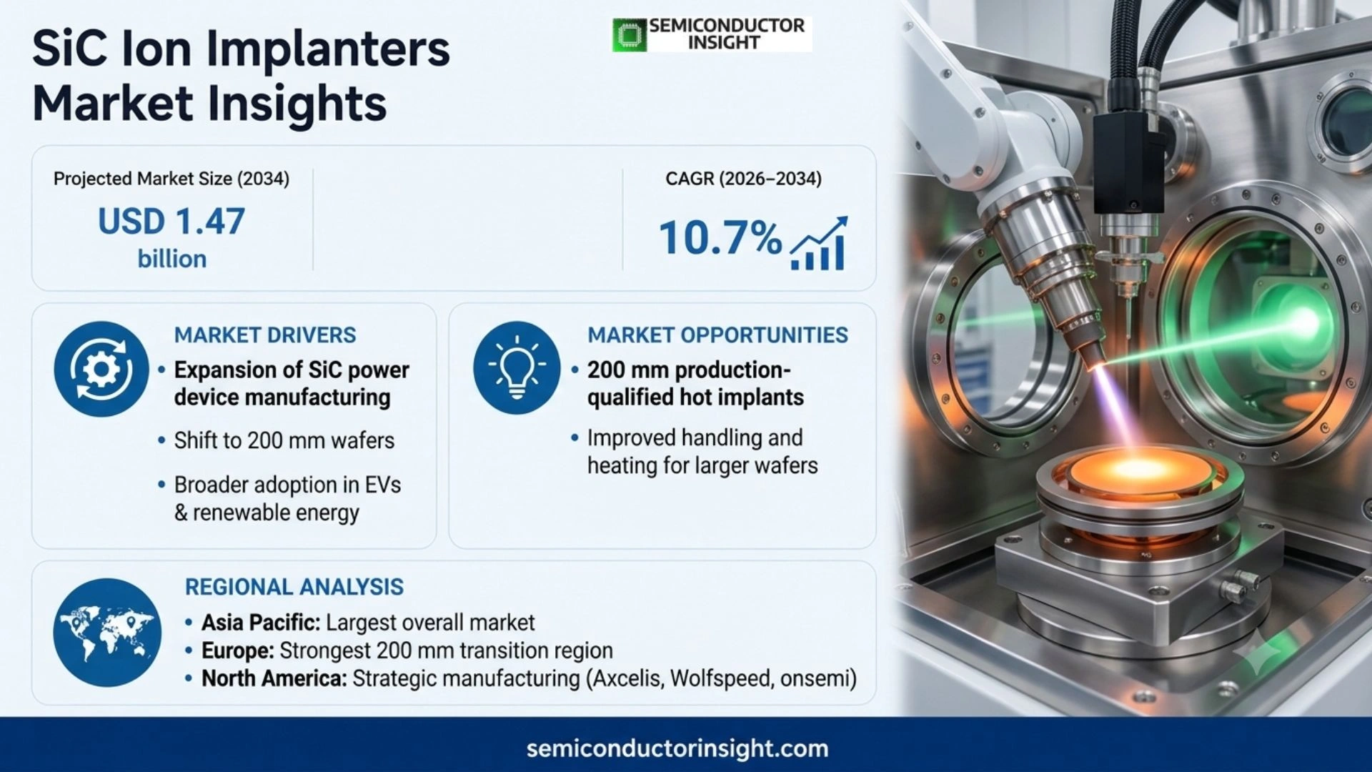
- Asia Pacific is the largest regional market, led by China and Japan and supported by major power-device capacity in Malaysia, Japan, China and South Korea. Europe is a high-value growth market because Infineon and STMicroelectronics are expanding 200 mm SiC production, while North America remains strategically important through Wolfspeed, onsemi and Axcelis.
- Axcelis is the market’s most visible dedicated SiC implant supplier and in September 2025 launched the Purion Power Series+ covering high-current medium-energy, medium-current and high-energy SiC implant requirements for both 150 mm and 200 mm wafers.
- Equipment qualification and thermal wafer handling are the major barriers to entry. SiC implantation requires high beam energy, aluminum or nitrogen species, elevated wafer temperatures, low particle generation, angle control and reliable handling of expensive wafers, limiting the number of suppliers capable of high-volume production performance.
SiC Ion Implanters Market Overview
SiC ion implanters market was valued at approximately USD 587.0 million in 2025 and is projected to reach approximately USD 1.47 billion by 2034, representing a 10.7% CAGR during 2026–2034. Asia Pacific is the largest regional market, supported by large-scale power-semiconductor manufacturing and by rapid investment in 150 mm and 200 mm silicon-carbide device capacity across China, Japan, South Korea and Malaysia.
A SiC ion implanter is specialized semiconductor manufacturing equipment used to introduce controlled dopants into silicon-carbide wafers. The tool extracts ions such as aluminum, nitrogen, phosphorus or boron, accelerates them to defined energies and scans the ion beam across the wafer to create precise concentration profiles. Unlike silicon, SiC has extremely low dopant diffusivity, so conventional thermal diffusion cannot form many required junction profiles efficiently. Ion implantation is therefore a core process for manufacturing SiC MOSFETs, diodes and other power devices.
The process is technically difficult because implantation can damage the SiC crystal lattice, and that damage is difficult to repair even with high-temperature annealing. Nissin explains that SiC wafers are often heated to around 500°C during implantation to reduce defect formation, while Applied Materials uses an integrated hot-implant capability in its VIISta 900 3D platform. Equipment must combine high beam energy, stable dose control, wafer heating, temperature uniformity and robust handling without introducing particles or warpage.
The market is also being reshaped by the transition from 150 mm to 200 mm SiC manufacturing. Larger wafers increase die output per process cycle, but they create additional handling and thermal-uniformity challenges because SiC wafers are expensive, mechanically demanding and sensitive to nonuniform heating. Infineon released its first products based on 200 mm SiC manufacturing technology in 2025, Wolfspeed commercially launched 200 mm SiC materials in September 2025 and STMicroelectronics stated that 200 mm SiC production in Catania was planned to begin in the fourth quarter of 2025.
Equipment differentiation increasingly depends on complete recipe coverage. SiC device flows use high-current implants for source/drain and body-related steps, medium-current implants for precision profiles and high-energy implants for deeper regions. Axcelis’ Purion Power Series+ therefore spans H200+ SiC, M+ SiC, XE+ SiC and EXE+ SiC variants, while other suppliers use dedicated high-temperature or multi-energy platforms. A customer that can qualify one equipment family across several implant steps can reduce maintenance, training and spare-parts complexity across the fab.
Segment Analysis: By Type
By wafer size, the market is segmented into 150 mm SiC Ion Implanters, 200 mm SiC Ion Implanters and Others. 150 mm equipment remains the larger installed base because much of current SiC production was originally built around 6-inch wafers. 200 mm is the fastest-growing segment as leading manufacturers qualify larger substrates and new fabs are designed around improved wafer economics.
| Type | Manufacturing role and requirements | Market position |
|---|---|---|
| 150 mm SiC Ion Implanters | Six-inch SiC production remains widely installed across automotive and industrial power-device fabs. Equipment must support high-temperature aluminum and nitrogen implantation, accurate dose control and high utilization on mature device architectures. Existing 150 mm fabs benefit from fully qualified process recipes and established wafer handling. | Largest installed-base segment. Replacement, capacity expansion and process upgrades remain significant because large portions of current commercial SiC MOSFET and diode output still use 150 mm wafers. Customers prioritize productivity and uptime rather than changing wafer size solely for equipment modernization. |
| 200 mm SiC Ion Implanters | Eight-inch implanters process larger, more valuable wafers and require tighter temperature uniformity, stable electrostatic clamping and reliable transfer. Applied Materials VIISta 900 3D supports 150 mm and 200 mm SiC, Axcelis Power Series+ supports both sizes, and Nissin IMPHEAT-II supports up to 8 inches. | Fastest-growing type. Infineon, Wolfspeed, STMicroelectronics and other manufacturers are moving toward 200 mm SiC. Greenfield production lines increasingly want equipment that is production-proven at 200 mm and can support future trench and superjunction devices. |
| Others | Includes R&D wafer sizes, small-sample processing and specialty systems used for process development or non-standard substrates. Some implanters can also handle Si, GaN, GaAs or emerging wide-bandgap materials in addition to SiC, improving equipment utilization in research or multi-product facilities. | A smaller segment with strategic relevance. Research centers and pilot fabs use flexible tools to develop implant species, thermal conditions and device structures before transferring recipes to high-volume 150 mm or 200 mm equipment. |
Implant-energy and current segmentation
A second segmentation divides the market into high-current medium-energy, medium-current and high-energy implanters. Axcelis’ 2025 Purion Power Series+ formalizes this structure: the H200+ SiC addresses high-current medium-energy requirements, M+ SiC serves medium-current processes and XE+/EXE+ SiC address high-energy steps. Device architecture determines which systems are required, and advanced trench or superjunction structures can increase demand for higher energy, tilt capability and more precise beam-angle control.
Segment Analysis: By Application
By application, the market is segmented into SiC Power Devices and Others. SiC power devices overwhelmingly dominate because ion implantation is fundamental to defining doped regions in MOSFETs, Schottky-related structures, JBS diodes and other high-voltage devices. Research and specialty applications remain smaller but support process innovation, new materials and early qualification of future device architectures.
| Application | Demand characteristics |
|---|---|
| SiC Power Devices | Dominant application. EV traction inverters, onboard chargers, DC fast charging, photovoltaic inverters, industrial drives, rail and AI data-center power conversion all use SiC devices where switching efficiency and high-voltage performance justify higher semiconductor cost. Manufacturing requires repeated implants of acceptor and donor species with accurate depth, dose and lateral placement. |
| Automotive SiC MOSFETs | Automotive devices require high yield, strict process control and long-term equipment stability because the end products undergo demanding qualification. As manufacturers migrate toward trench MOSFETs and lower specific on-resistance, implant-angle control and crystal-damage management become increasingly important. |
| Renewable Energy and Industrial Power | Solar inverters, energy storage, industrial motor drives and charging infrastructure create a diversified demand base beyond vehicles. These products often use high-voltage SiC MOSFETs or diodes and can absorb fab capacity when automotive cycles soften, supporting sustained implanter utilization. |
| AI Data Center Power | AI servers and power-distribution systems are increasing demand for higher-efficiency power conversion. SiC is relevant in medium-voltage conversion, UPS, power supplies and grid infrastructure, creating a newer downstream growth path that reinforces long-term investment in SiC device fabs. |
| Others / R&D | Universities, national laboratories, process-development centers and equipment suppliers use SiC ion implantation for material studies, new device architectures and novel dopants. These systems typically prioritize flexibility and diagnostics over highest production throughput. |
Device-architecture segmentation
The market can also be analyzed across planar MOSFET, trench MOSFET, superjunction and diode-related process flows. Planar devices use established implant recipes, while trench and superjunction approaches may require deeper implants, more complex tilt angles or tighter lateral placement. Axcelis positions the Purion Power Series+ as covering planar, trench and emerging superjunction SiC devices, showing that architecture evolution is becoming an important equipment-upgrade trigger.
Regional Analysis
Asia Pacific is the largest SiC ion implanter market, Europe is the strongest 200 mm transition region, and North America remains strategically important through Axcelis, Wolfspeed, onsemi and U.S. power-semiconductor manufacturing. Regional demand follows actual SiC wafer-fab construction and technology migration. China and Japan have large equipment and device ecosystems, Malaysia is adding major 200 mm capacity, and Europe is investing aggressively in automotive-oriented SiC manufacturing.
How does regional SiC implanter demand differ?
Asia Pacific combines domestic equipment manufacturers with a large installed base of power-semiconductor fabs. Europe is highly concentrated around automotive and renewable-energy demand and is moving quickly to 200 mm production through Infineon and STMicroelectronics. North America benefits from Wolfspeed, onsemi and equipment suppliers such as Axcelis and Applied Materials. Emerging regions have limited direct SiC implantation today because the equipment only becomes economically attractive when a region has a meaningful front-end wafer-fabrication base.
| Region | Position | Growth outlook | Demand profile | What decides supplier selection |
|---|---|---|---|---|
| Asia Pacific | Largest | High | China/Japan device manufacturing and 200 mm expansion led | Throughput, high-temperature reliability, local service, 200 mm handling and price |
| Europe | High-value growth market | Very high | Automotive SiC and 200 mm transition led | Process performance, trench capability, qualification, lifecycle and local support |
| North America | Strategic equipment and fab market | High | Wolfspeed/onsemi capacity and equipment innovation led | Recipe coverage, productivity, process support and trusted supply |
| South America | Nascent | Low to moderate | Research and downstream power electronics led | Project economics, imported equipment and technical support |
| Middle East & Africa | Emerging | Low to moderate | Research, renewable energy and early semiconductor investment led | Local fab pipeline, service capability and project bankability |
Key SiC Ion Implanter Manufacturers and Competitive Landscape
Competition is highly concentrated because SiC implantation requires specialized beamline, hot-wafer handling, electrostatic clamping, angle control and contamination management. Axcelis has the most visible dedicated SiC portfolio across several current and energy ranges. Applied Materials, Nissin Ion Equipment, ULVAC and Sumitomo Heavy Industries Ion Technology provide additional production-capable ion-implant platforms, while Chinese equipment companies are expanding alongside domestic SiC manufacturing.
The competitive test is production yield rather than beam energy alone. Customers evaluate wafer temperature stability, dose uniformity, particle performance, beam-angle accuracy, species-change time, maintenance intervals and throughput on expensive SiC wafers. A tool that reduces crystal damage or handles warped 200 mm wafers more reliably can improve downstream activation and device yield enough to justify a higher capital price.
Installed-base compatibility is another advantage. Fabs prefer common spare parts, recipes, service procedures and operator training across high-current, medium-current and high-energy implants. Axcelis’ platform strategy explicitly targets complete recipe coverage, while Nissin develops SiC tools from proven semiconductor implanter families. Suppliers with local service teams and process-development centers can therefore win follow-on systems after the first qualification.
Key Industry Players
- Axcelis Technologies
- Applied Materials
- Nissin Ion Equipment Co., Ltd.
- ULVAC
- Sumitomo Heavy Industries Ion Technology Co., Ltd.
- CETC-48
- Shanghai Kingstone Semiconductor Corporation
- IBS / Ion Beam Services
- Foshan Jihua
- Qingdao Sifang SRI Intellectual Technology
SiC Ion Implanter Production Capacity Analysis
Production capacity for SiC ion implanters is constrained by precision beamline manufacturing, high-voltage power supplies, magnets, vacuum systems, ion sources, electrostatic chucks, wafer-heating assemblies and extensive factory acceptance testing. These tools are built in relatively low unit volumes compared with mainstream semiconductor process equipment, so supplier capacity depends heavily on skilled engineering and long-lead subsystems rather than high-speed repetitive assembly.
Axcelis has expanded the Purion platform through dedicated SiC variants and supports 150 mm and 200 mm wafers across multiple energy classes. Nissin produces high-temperature IMPHEAT-II systems in Japan, ULVAC offers dedicated IH-series SiC implanters including a 200 mm IH-1200PSIC, and Applied Materials supplies VIISta 900 3D with integrated hot implant. This supplier diversity improves availability, but the number of proven high-volume platforms remains limited relative to total semiconductor equipment categories.
The transition to 200 mm affects effective capacity because larger wafers require updated handling, heating and qualification. A supplier may have manufacturing capability for a 150 mm tool but still need extensive engineering to prove wafer-temperature uniformity and low breakage at 200 mm. Customers also require recipe demonstrations on their actual wafer types and implant species before accepting the system, extending the time between factory build and productive fab capacity.
Service capacity can become a practical bottleneck as the installed base expands geographically. Ion implanters require beam tuning, source maintenance, high-voltage service and regular process calibration. SiC fabs in new regions therefore prefer vendors with local engineers, spare ion-source components and remote diagnostic capability. Equipment suppliers that expand service centers alongside tool shipments can convert manufacturing capacity into usable customer capacity more effectively.
SiC Ion Implanters Market Dynamics: Drivers, Restraints and Opportunities
Market growth is driven by expansion of SiC power-device manufacturing, the shift to 200 mm wafers, trench and superjunction architectures and broader adoption of SiC in EVs, renewable energy, industrial systems and AI data-center power. Restraints include high equipment cost, long qualification cycles, SiC device-market cyclicality and a limited supplier base. The strongest opportunities lie in 200 mm hot implant, complete recipe coverage, higher throughput and locally supported equipment for new Asian and European fabs.
MARKET DRIVERS
Drivers Impact Analysis*
| Market Factor | Directional Impact on CAGR Forecast* | Commercial Mechanism |
|---|---|---|
| Global SiC power-device capacity expansion | +2.2 to +3.0 percentage points | EV, renewable-energy and industrial demand supports new SiC fabs and additional implant tools across multiple doping steps. |
| Transition from 150 mm to 200 mm wafers | +1.5 to +2.1 percentage points | New 200 mm lines require production-qualified hot implant systems and can trigger replacement or greenfield purchases. |
| Advanced trench and superjunction architectures | +0.9 to +1.4 percentage points | More complex devices require higher energy, tilt, precise angle and broader recipe coverage, increasing equipment value per fab. |
SiC fab expansion creates direct equipment demand
Ion implantation is a required front-end process for many SiC power-device structures, so new wafer capacity translates directly into tool demand. Infineon, STMicroelectronics, Wolfspeed and other manufacturers are expanding or modernizing SiC operations. Each new line requires several implant energy and current capabilities, and high-volume fabs need redundancy and spare capacity to maintain output during maintenance.
200 mm migration triggers a new qualification cycle
A fab moving from 150 mm to 200 mm cannot simply reuse every existing tool unchanged. Wafer transport, heating, electrostatic chuck design, beam uniformity and mechanical tolerances must be proven on the larger substrate. Wolfspeed’s commercial 200 mm materials launch and Infineon’s 200 mm product rollout demonstrate that the wafer transition is already moving into production, creating a clear demand window for 200 mm-capable implanters.
Hot implantation improves device performance and yield
SiC’s crystal structure makes room-temperature implantation damaging, while post-implant diffusion is extremely limited. Applied Materials demonstrated that hot implantation can reduce resistivity by more than 40 times compared with room-temperature implant in its development work. Nissin supports up to 500°C in IMPHEAT-II. These process benefits make high-temperature control a central equipment differentiator and support premium system pricing.
New device architectures require broader recipe coverage
As power-device designers move toward trench gates and superjunction concepts, implant profiles become more demanding. Axcelis’ Power Series+ was launched specifically to address planar, trench and emerging superjunction requirements across different current and energy ranges. A broader recipe envelope can allow one supplier to capture several tool positions in the same new fab.
MARKET RESTRAINTS
Restraints Impact Analysis*
| Market Factor | Directional Impact on CAGR Forecast* | Commercial Mechanism |
|---|---|---|
| High equipment price and low annual unit volume | −1.2 to −1.8 percentage points | Specialized beamline and hot-wafer hardware create high capital cost, limiting buyers to serious power-semiconductor manufacturers. |
| Long process qualification and delivery cycles | −0.9 to −1.4 percentage points | Fabs require species-, dose-, temperature- and device-specific qualification before tools enter production, delaying revenue recognition. |
| SiC device-market and EV cyclicality | −0.6 to −1.0 percentage points | Power-device customers can defer capacity additions when EV or industrial demand softens, creating uneven equipment order cycles. |
A specialized SiC tool is a major capital commitment
High-temperature implanters include complex vacuum, ion-source, magnet, heating and high-voltage systems and are sold in far lower quantities than commodity manufacturing equipment. Customers therefore need a clear capacity plan before ordering. Research organizations may use implantation services rather than purchase a full production system, which limits the potential customer base outside major fabs.
Qualification can take longer than mechanical installation
A tool must demonstrate implant dose, energy, angle, particle performance, temperature uniformity and downstream electrical results using the customer’s actual device flow. Changing from one equipment platform to another can require extensive recipe redevelopment and reliability validation. This favors incumbent suppliers but slows market-share shifts and can delay the commercial impact of new products.
SiC capital spending is sensitive to end-market timing
The long-term case for SiC remains strong, but EV inventory cycles and slower-than-expected vehicle programs can cause power-semiconductor manufacturers to adjust fab ramps. Equipment orders are therefore lumpy. A supplier may receive several systems for one expansion and then experience a period of lower demand until utilization catches up with installed capacity.
MARKET OPPORTUNITIES
200 mm production-qualified hot implant
The strongest near-term opportunity is equipment that proves stable high-temperature implantation on 200 mm SiC. Larger wafers create more device output but also increase handling and heating difficulty. Suppliers that demonstrate low breakage, uniform temperature and competitive throughput can win greenfield lines as manufacturers standardize future capacity around 200 mm.
Superjunction and advanced trench implantation
Emerging architectures can require deeper, more precisely shaped doped regions. High-energy systems, tilt capability and accurate beam-angle control therefore become more valuable. Axcelis has expanded its Power Series+ specifically for these device roadmaps, indicating a market opportunity where process complexity drives new equipment even without a large increase in wafer starts.
Localization of SiC equipment in China
China is investing in domestic SiC devices, substrates and semiconductor equipment. Local suppliers can capture demand through price, service and reduced import exposure, while established global vendors can compete through higher productivity and proven process results. The market can therefore expand both through new fabs and through localization of previously imported implant capability.
Implantation services and process-development centers
Not every device company can justify a dedicated implanter during early development. Nissin operates implantation services supporting SiC, GaN and Ga2O3, including high-temperature processing up to 600°C. Service centers create revenue from R&D customers and can also act as qualification environments that lead to later equipment purchases when products move into volume manufacturing.
SiC Ion Implanter Supply Chain Analysis
The supply chain spans high-voltage and beamline subsystems, implanter manufacturing, fab process integration and lifecycle service. Unlike wafer or chemical supply chains, the key upstream constraint is specialized engineering content. Magnets, ion sources, vacuum components, electrostatic chucks, heaters and precision motion systems must operate together with low contamination and stable beam characteristics over long production campaigns. Downstream value depends on how implantation affects activation, resistance and device yield after annealing.
Stage 1 – Ion source, beamline and vacuum subsystems
The implanter begins with an ion source that must generate stable beams for species such as aluminum and nitrogen. Magnets select the ion mass, acceleration stages set energy and diagnostics measure current and angle. SiC recipes can demand high doses or high energies, so component stability affects both throughput and repeatability. Specialized high-voltage and vacuum suppliers therefore influence equipment lead time and service performance.
Stage 2 – High-temperature wafer handling
The wafer must be heated while remaining mechanically stable and electrically controlled. Applied Materials uses an electrostatic clamp to improve temperature uniformity and manage warpage, Nissin supports up to 500°C in production IMPHEAT-II, and ULVAC offers high-temperature ESC-based SiC tools. This stage is one of the strongest technical barriers because particle generation or thermal nonuniformity directly affects expensive device wafers.
Stage 3 – Device recipe and anneal integration
Implantation does not create the final electrical junction by itself. Device manufacturers combine multiple energies and doses to form a profile and then use high-temperature annealing to activate dopants and repair damage. The implanter supplier therefore works closely with process integration teams. A recipe that appears uniform physically can still fail electrically if crystal damage or activation produces excessive resistance.
Stage 4 – Lifecycle service and utilization
Ion sources and beamline components require maintenance, and high-temperature hardware adds another wear mechanism. Customers value fast source changes, stable calibration and local service because implanter downtime can halt several critical device layers. Suppliers with installed-base analytics, spare parts and regional application engineers can achieve higher customer utilization and stronger repeat orders.
Recent Developments in the SiC Ion Implanters Market
Axcelis introduced the Purion Power Series+ platform with H200+ SiC, M+ SiC, XE+ SiC and EXE+ SiC variants. The platform supports 150 mm and 200 mm wafers and room-temperature, warm and hot implantation, extending recipe coverage for planar, trench and emerging superjunction power-device structures.
Wolfspeed announced commercial availability of 200 mm SiC bare wafers and immediate availability of 200 mm epitaxy for qualification. The move supports industry-scale transition to larger wafer sizes and creates downstream demand for 200 mm-capable ion implantation, annealing, etch and inspection equipment.
STMicroelectronics said development of its Silicon Carbide Campus in Catania was progressing as planned and that production on 200 mm wafers was expected to begin in the fourth quarter of 2025. The transition increases demand for production-qualified 200 mm SiC front-end tools, including hot ion implanters.
Infineon announced that first products manufactured using its advanced 200 mm SiC wafer technology in Villach would be released to customers in the first quarter of 2025. The company also said conversion of its Kulim, Malaysia site from 150 mm to 200 mm SiC was on track, reinforcing the equipment transition toward larger wafers.
Axcelis announced multiple first-quarter shipments of Purion Power Series implanters to leading SiC chipmakers worldwide. The systems included H200 SiC high-current, XE SiC high-energy and M SiC medium-current models for high-volume power-device manufacturing across automotive, industrial and energy applications.
REPORT SCOPE & SEGMENTATION
| Study Period | 2019–2034 |
| Base Year | 2025 |
| Estimated Year | 2026 |
| Forecast Period | 2026–2034 |
| Historical Period | 2019–2025 |
| Market Size 2025 | USD 587.0 Million |
| Market Size 2034 | USD 1.47 Billion |
| Growth Rate | CAGR of 10.7% from 2026–2034 |
| Largest Market 2025 | Asia Pacific |
| Unit | Value (USD Million/Billion) and equipment units |
| Segmentation | By Wafer Size, Implant Class, Application, Device Architecture and Region |
| By Wafer Size | 150 mm SiC Ion Implanters · 200 mm SiC Ion Implanters · Others |
| By Implant Class | High-Current Medium-Energy · Medium-Current · High-Energy |
| By Application | SiC Power Device · Research and Others |
| By Device Architecture | Planar MOSFET · Trench MOSFET · Superjunction · Diode and Other Structures |
| By Region | North America · Europe · Asia Pacific · South America · Middle East & Africa |
| Companies Profiled | Axcelis Technologies · Applied Materials · Nissin Ion Equipment Co., Ltd. · ULVAC · Sumitomo Heavy Industries Ion Technology Co., Ltd. · CETC-48 · Shanghai Kingstone Semiconductor Corporation · IBS / Ion Beam Services · Foshan Jihua · Qingdao Sifang SRI Intellectual Technology |
| Customization Scope | Country, wafer size, implant species, energy/current class, temperature range, device architecture, fab project and company-level customization can be added for customer-specific SiC manufacturing requirements. |
Frequently Asked Questions
What is the size of the SiC ion implanters market in 2025?
The global SiC ion implanters market was valued at approximately USD 587.0 million in 2025. The market includes dedicated and multi-purpose ion implantation systems used for high-temperature and high-energy doping of silicon-carbide wafers in power-device manufacturing.
What is the projected market size by 2034?
The market is projected to reach approximately USD 1.47 billion by 2034, representing a 10.7% CAGR during 2026–2034. Growth is supported by SiC fab expansion, 200 mm wafer migration and more complex power-device structures.
Which region leads the SiC ion implanter market?
Asia Pacific is the largest market because China and Japan have large semiconductor-equipment and power-device ecosystems and Malaysia is adding major 200 mm SiC capacity. Europe is also growing rapidly through Infineon and STMicroelectronics investments.
Which wafer-size segment is growing fastest?
200 mm SiC ion implanters are the fastest-growing segment. Wolfspeed commercially launched 200 mm SiC materials in 2025, Infineon began releasing 200 mm SiC products and ST is advancing 200 mm production in Catania.
Why does SiC require high-temperature ion implantation?
Dopants diffuse very slowly in SiC and room-temperature implantation can heavily damage the crystal lattice. Heating the wafer during implantation reduces damage and improves downstream activation. Production systems from Nissin, Applied Materials, Axcelis and ULVAC therefore include hot-implant capability.
What ions are commonly implanted into SiC?
Common species include aluminum for p-type regions and nitrogen or phosphorus for n-type regions, with other species used for specialized structures. Device makers often combine several implant energies to build the required concentration profile.
What are the main market restraints?
The main restraints are high equipment cost, long tool and recipe qualification, limited supplier availability and cyclical SiC capacity spending. High-temperature wafer handling and expensive substrates also raise the technical and financial risk of production ramp.
Which companies are profiled?
The report profiles Axcelis Technologies, Applied Materials, Nissin Ion Equipment, ULVAC, Sumitomo Heavy Industries Ion Technology, CETC-48, Shanghai Kingstone Semiconductor, IBS / Ion Beam Services, Foshan Jihua and Qingdao Sifang SRI.
How does trench SiC affect equipment demand?
Trench and emerging superjunction structures can require more demanding implant energy, tilt and angle control than established planar devices. This increases the value of high-energy and flexible implanter platforms and can create new equipment purchases even in existing fabs.
What is the strongest long-term opportunity?
The strongest opportunities are production-qualified 200 mm hot implantation, broader recipe coverage across high-current and high-energy steps, advanced trench/superjunction processes and localized equipment/service capability near new SiC fabs.

Get Sample Report PDF for Exclusive Insights
Report Sample Includes
- Table of Contents
- List of Tables & Figures
- Charts, Research Methodology, and more...