Key Statistics
The SiC MOSFET chips, devices and module market is entering a scale phase in which automotive inverters, charging infrastructure, renewable-energy conversion and industrial power systems increasingly value higher switching efficiency and thermal operating margins. The demand mechanism is moving from discrete component substitution toward platform-level qualification, where device suppliers must prove reliability at system voltage, switching frequency and thermal conditions. This raises the commercial value of process maturity, package design, wafer economics and long-term customer support alongside electrical performance.
Key Takeaways
- SiC MOSFET chips/devices remain the core product category, while module adoption expands where customers need higher integration, lower parasitics and simplified thermal management in traction, charging, UPS and industrial power platforms.
- Automotive is the most strategically important end industry, with electric-car sales exceeding 17 million globally in 2024 according to the IEA; China alone sold more than 11 million electric cars, enlarging the addressable base for high-voltage power conversion.
- Asia-Pacific combines the strongest production and consumption ecosystem, while Europe is intensifying localized 200 mm SiC manufacturing and North America is building vertically integrated materials-and-device capacity.
- The central growth driver is the need to reduce conversion losses across higher-voltage architectures; the restraint is the still-high cost and manufacturing complexity of SiC substrates, epi, defect control and high-yield device fabrication.
- Competitive advantage is shifting toward 200 mm wafer capability, vertically integrated substrate-to-module operations, automotive qualification and package-level innovation that can turn lower device losses into measurable system efficiency.
SiC MOSFET Chips (Devices) and Module Market Overview
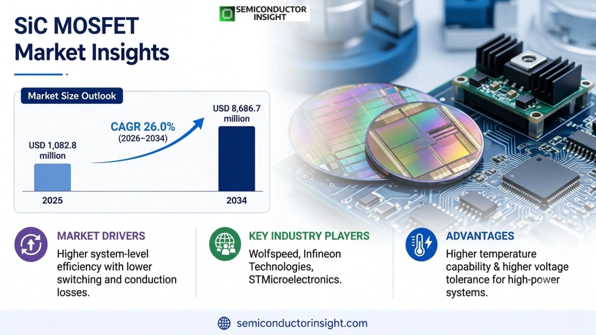
SiC MOSFET chips devices and module market was valued at USD 540.9 million in 2022 and was reported at USD 2,731.9 million for 2029. Rebasing those published anchors to the requested 2025–2034 window gives a 2025 market size of USD 1,082.8 million, a 2034 value of USD 8,686.7 million and a 26.0% CAGR for 2026–2034. The market includes SiC MOSFET chips/devices and SiC MOSFET modules used in automotive, industrial, energy and communications power-conversion systems.
SiC MOSFETs use silicon carbide as the semiconductor platform for power switching where lower conduction and switching losses, higher temperature capability and higher voltage tolerance can improve system-level efficiency. The commercial purchase is rarely made on chip price alone: vehicle OEMs, inverter makers, charging-system suppliers and industrial equipment vendors evaluate electrical characteristics, short-circuit robustness, gate-drive behavior, package inductance, thermal performance, reliability qualification and long-term availability. Suppliers therefore compete through a combination of wafer yield, device architecture, packaging and application engineering.
The technology architecture spans a materials chain that begins with high-purity SiC powder, crystal growth and wafer preparation, then continues through epitaxy, MOSFET fabrication, thinning, metallization, dicing and module assembly. Every stage can influence cost and yield. Larger wafer formats increase the number of dies available per processing cycle, while improved defect inspection and epitaxial control can reduce scrap. At the downstream end, low-inductance packages, sintered interconnects and thermal paths determine how much of the semiconductor’s intrinsic performance can actually be captured in the finished inverter, power supply or module.
Demand is changing now as electrification, renewable generation and power-hungry digital infrastructure raise the importance of efficient conversion. The IEA reported more than 17 million electric cars sold globally in 2024, with China accounting for more than 11 million, a scale that expands the installed base of traction inverters and on-board charging systems. At the same time, suppliers are developing 200 mm SiC manufacturing, higher-voltage platforms and more compact surface-mount packages, signaling a move from early-adopter positioning toward cost and manufacturability as competitive priorities.
Segment Analysis: By Type
The source report defines two product types: SiC MOSFET Chip and Device, and SiC MOSFET Module. Chip/device products address component-level switching requirements and allow system designers to optimize their own packaging and thermal architecture, while modules integrate multiple semiconductor elements and interconnects into a higher-level power building block. Chip/device volume remains foundational to the ecosystem, yet module growth can accelerate where automotive and industrial customers value shorter design cycles, lower parasitic inductance and integrated thermal management.
| Type | Demand and Commercial Characteristics | Position |
|---|---|---|
| SiC MOSFET Chip and Device | Primary device category used across traction inverters, industrial power supplies, renewable-energy converters and telecom power stages. Device suppliers compete on voltage class, on-resistance, switching loss, body-diode behavior, short-circuit robustness and automotive qualification. Toshiba’s 2025 launches of 650 V third-generation devices show the continuing push toward compact surface-mount implementations that improve power density in industrial equipment and photovoltaic power conditioners. | Largest / foundational |
| SiC MOSFET Module | Integrated assemblies that combine SiC dies with package-level electrical and thermal structures. Modules are attractive in traction inverters, industrial drives, renewable-energy converters and other high-current systems where electrical loop inductance, thermal interfaces and mechanical reliability are difficult to optimize from discrete parts. ST’s vertical SiC strategy and its module production roadmap illustrate how module capability increasingly connects wafer manufacturing to system-level customer qualification. | Fast strategic expansion |
Secondary technology lens: wafer diameter and package integration
The most consequential secondary axis is the manufacturing and package platform supporting each device type. Infineon began customer rollout of products manufactured on advanced 200 mm SiC wafers in Villach in the first quarter of 2025 and was progressing with 200 mm conversion in Kulim, while ST’s Catania campus was designed around 200 mm SiC manufacturing and integrated substrate, device, test and packaging capabilities. These moves matter commercially: a larger wafer can raise die counts per wafer, and tighter vertical integration can reduce dependence on external substrate supply and shorten process-learning loops.
Segment Analysis: By Application
| Application | Demand Characteristics and Purchasing Trigger |
|---|---|
| Motor Drives | Purchasing is triggered by the need to improve motor efficiency, reduce cooling burden and maintain performance under high-frequency switching. Industrial drive makers evaluate conduction loss, switching behavior, ruggedness and lifecycle availability, while suppliers differentiate through application reference designs and package choices that fit inverter footprints. Adoption can expand gradually across pumps, compressors, robotics and factory automation once a qualified device proves repeatable field performance. |
| Industrial Power Supplies | The trigger is higher power density within constrained cabinet or rack volume. SiC enables higher switching frequency and lower loss, allowing designers to reduce magnetics or cooling requirements when the complete topology is optimized. Suppliers therefore compete on switching loss at application-relevant temperatures, gate-control behavior, package parasitics and second-source availability, not merely the headline voltage rating. |
| Electric Vehicle (EV) Charging Stations | Charging operators and equipment manufacturers purchase SiC when conversion efficiency, thermal density and high-voltage operation can improve charger size, operating cost or charging performance. The commercial decision often starts with a 650 V, 750 V or 1,200 V class architecture and then moves into qualification of the exact die and package combination. Toshiba’s 650 V devices and broad supplier movement into higher-current modules demonstrate how package density is becoming as important as semiconductor efficiency. |
| Traction Inverters | This application has the strongest system-level incentive to use SiC where lower inverter losses can support range, thermal headroom or smaller cooling systems. Automotive customers impose the toughest qualification, traceability and longevity requirements, which favors suppliers with automotive-grade process control and established module integration. ROHM’s fourth-generation SiC MOSFET bare dies being adopted in three ZEEKR models illustrates how design-in relationships can convert device performance into recurring series-production demand. |
| UPS and SMPS | UPS and switch-mode power-supply designers focus on efficiency, switching frequency and thermal stability. SiC MOSFETs can support compact high-frequency stages, and the value rises in power systems where heat removal is expensive or rack density is constrained. The opportunity increasingly extends beyond traditional industrial supplies into data-center power architectures, where suppliers are adapting high-voltage SiC switching technologies to improve conversion efficiency in AI infrastructure. |
| Industrial Photovoltaic (PV) | Solar inverter makers value high efficiency over a broad load range, high-voltage blocking capability and reliable operation under thermal stress. SiC devices can reduce switching losses and support more compact magnetics and cooling structures. Toshiba’s 650 V product family is explicitly positioned for power conditioners for photovoltaic generators, illustrating the role of surface-mount packaging and power density in moving SiC from performance-focused designs toward commercially optimized equipment platforms. |
| Other | Other uses span telecommunications power conversion, aerospace and defense power systems, energy storage and emerging high-frequency converters. Purchasing remains application-specific, with qualification centered on voltage, temperature, switching waveform, reliability and package behavior. These niches can be strategically valuable even when they are smaller in volume, since high-reliability applications reward suppliers that can document long qualification histories and maintain consistent process control over extended product lifetimes. |
Regional Analysis
Asia-Pacific holds the strongest structural position in the SiC MOSFET market due to the concentration of semiconductor manufacturing, power-electronics supply chains and electric-vehicle production across China, Japan and South Korea. North America combines a large EV and renewable-energy customer base with an increasingly localized SiC materials and wafer ecosystem. Europe is distinguished by automotive design concentration and accelerating regional 200 mm production, while South America and the Middle East & Africa remain smaller but increasingly relevant as renewable-energy and electrification investments expand.
| Region | Commercial Position | Why the Region Behaves Differently | Evidence / Market Instance | Growth Outlook |
|---|---|---|---|---|
| Asia-Pacific | Largest regional ecosystem | China, Japan and South Korea combine manufacturing scale, automotive demand and power-electronics specialization. The commercial mechanism is ecosystem density: device makers, module suppliers, inverter manufacturers and vehicle programs are geographically proximate, supporting faster qualification and higher production learning. | China sold more than 11 million electric cars in 2024 according to IEA, while ROHM’s supply relationship with ZEEKR demonstrates direct SiC device integration into Chinese EV platforms. | Fastest structural expansion |
| North America | High-value demand plus vertical integration | The region combines EV, charging, renewable-energy and data-center power demand with a strong domestic SiC manufacturing base. Wolfspeed’s 200 mm Mohawk Valley fab and North Carolina materials expansion create a vertically oriented supply position, while onsemi continues to broaden its high-voltage SiC portfolio. | Wolfspeed describes Mohawk Valley as a fully automated 200 mm SiC fab; onsemi’s 2025 Qorvo JFET acquisition added SiC technology and was announced at USD 115 million. | High |
| Europe | Automotive qualification and 200 mm transition | Europe’s commercial center of gravity is automotive electrification and industrial power conversion, supported by a dense engineering base. Infineon’s Villach products made from 200 mm SiC wafer manufacturing began customer rollout in Q1 2025, while ST is building a vertically integrated 200 mm campus in Catania. | Infineon cites high-voltage applications including renewables, trains and EVs; ST’s Catania plan combines substrate, device, test and packaging on one site. | High |
| South America | Renewable-energy-led adoption | Demand is more project-led than fab-led, with solar generation, grid modernization and industrial electrification creating the main purchasing triggers. The region generally depends on imported SiC devices and modules, making distributor capability, application support and availability especially important. Suppliers with certified devices and a broad voltage range can win positions through inverter and power-conversion programs rather than local wafer manufacturing. | Solar and industrial power conversion create the most defensible entry points, with automotive adoption following the expansion of charging infrastructure and electrified transport. | Medium |
| Middle East & Africa | Grid, solar and high-temperature power needs | The regional opportunity is driven by renewable-energy projects, grid-support equipment, transport electrification and high-ambient-temperature applications. System buyers value thermal robustness and long service life, which can favor SiC in applications where cooling is difficult. The supply model remains import-heavy, so local technical representation, inventory and project qualification are essential components of the commercial offer. | Large solar and grid projects create opportunities for high-voltage switching devices and modules, while harsh ambient conditions strengthen the value proposition of high-temperature-capable wide-bandgap power electronics. | Medium-high |
How is manufacturing density translating into SiC MOSFET demand?
Asia-Pacific’s advantage comes from the overlap of device production, automotive manufacturing and power-electronics assembly. China, Japan and South Korea are not merely end markets; they are interconnected production centers. This shortens qualification loops and supports rapid design-in when EV platforms, charging systems or industrial converters move from engineering samples to volume production. Suppliers therefore compete on localized engineering support and production continuity as much as on electrical specifications.
| Country | Position | Demand Mechanism |
|---|---|---|
| China | Largest manufacturing and consumption center | EV, charging and power electronics scale create a dense device-to-system chain. IEA’s 2024 electric-car sales figure of more than 11 million shows the customer base supporting traction and charging applications. |
| Japan | Advanced device engineering base | ROHM, Toshiba and Mitsubishi Electric anchor a mature power-semiconductor ecosystem where high-reliability industrial and automotive design-ins reward process consistency and long qualification histories. |
| South Korea | Automotive and electronics demand | South Korea’s automotive, battery and electronics ecosystem creates opportunities for SiC in traction, charging and industrial power conversion, with local engineering relationships influencing device selection. |
Market instances
- 2024 — IEA reported more than 17 million electric cars sold globally and more than 11 million in China. This matters for SiC suppliers because traction inverters and charging systems provide a high-volume route from device qualification to recurring production demand.
- 2024 — ROHM reported that its fourth-generation SiC MOSFET bare dies were adopted in the traction inverters of three ZEEKR EV models. The development demonstrates how device qualification with one vehicle platform can create repeat demand across multiple models.
- 2025 — Toshiba launched four 650 V third-generation SiC MOSFETs in DFN8×8 packages and began volume shipments immediately. The package reduces device volume by more than 90% versus referenced through-hole packages, linking SiC efficiency to power-density gains in industrial equipment and PV power conditioners.
The regional implication is specific to Asia-Pacific: suppliers should align inventory, application engineering and qualification resources with the region’s dominant purchase mechanism rather than apply a generic global playbook. This block uses the region’s manufacturing base, customer mix, project structure and access conditions to explain why demand converts differently into revenue. In the full report, country-level sizing, supplier positions, application splits and company comparisons should be read alongside the headline market series for investment and sourcing decisions.
How does localized SiC manufacturing affect North American sourcing?
North America is building a supply proposition around domestic materials, 200 mm wafer fabrication and integrated device production. Wolfspeed’s Mohawk Valley and North Carolina projects provide a clear example of vertical manufacturing intent, while the region’s EV, renewable and data-center customers create premium demand for reliable high-voltage switching. The resulting commercial logic favors suppliers that can combine local support, capacity visibility and advanced wafer economics.
| Country | Position | Demand Mechanism |
|---|---|---|
| United States | Demand plus domestic capacity | The U.S. combines EV and renewable demand with Wolfspeed’s 200 mm materials-and-device ecosystem and onsemi’s expanding SiC technology portfolio. Local support and supply visibility are strategic buying factors. |
| Canada | Emerging power-conversion demand | Canada’s opportunity is concentrated in EV supply chains, renewable power and industrial electrification. Imported devices can win when suppliers provide robust qualification data and application support to local system integrators. |
| Mexico | Automotive manufacturing corridor | Mexico’s automotive manufacturing base creates a downstream route for SiC adoption through traction, charging and industrial power electronics. Supplier access depends on integration with North American OEM and Tier 1 qualification programs. |
Market instances
- 2024 — Wolfspeed reported progress at the Mohawk Valley 200 mm SiC fab and its North Carolina materials operation. The development matters for customers seeking a more integrated supply base, and it supports a commercial proposition built around wafer-scale economics, traceability and long-term capacity visibility.
- 2025 — onsemi completed the acquisition of Qorvo’s SiC JFET technology portfolio for USD 115 million. The deal expands device architecture options for high-energy-efficiency power systems and strengthens the supplier’s ability to address AI-data-center power supplies and EV battery-disconnect applications.
- 2024 — Wolfspeed reported an equipment incident at its Durham 150 mm device fab that temporarily reduced capacity before production resumed. The event illustrates the operational risk in specialized wide-bandgap fabs and reinforces the value of diversified footprints, process redundancy and customer qualification across multiple production sites.
The regional implication is specific to North America: suppliers should align inventory, application engineering and qualification resources with the region’s dominant purchase mechanism rather than apply a generic global playbook. This block uses the region’s manufacturing base, customer mix, project structure and access conditions to explain why demand converts differently into revenue. In the full report, country-level sizing, supplier positions, application splits and company comparisons should be read alongside the headline market series for investment and sourcing decisions.
What makes Europe strategically important despite a smaller production base than Asia?
Europe’s differentiation is rooted in automotive engineering, industrial automation and a dense network of customers that can convert device improvements into system-level requirements. Infineon’s Villach 200 mm rollout and ST’s Catania campus illustrate an effort to localize more of the SiC chain. This creates opportunities for suppliers able to demonstrate traceability, functional safety maturity and long-life manufacturing support.
| Country | Position | Demand Mechanism |
|---|---|---|
| Germany | Automotive-led demand | Germany’s automotive and industrial base supports advanced SiC design-ins, with efficiency and reliability requirements shaping inverter and power-supply specifications. Suppliers benefit from local applications engineering and documented automotive qualification. |
| Italy | Integrated 200 mm manufacturing | Italy is strategically important through ST’s Catania SiC campus, designed to combine substrate and device manufacturing with test and packaging. This creates a localized production and learning center for high-volume SiC. |
| Austria | 200 mm device ramp | Infineon’s Villach site began customer rollout of 200 mm SiC products in Q1 2025, strengthening Europe’s device-manufacturing position for high-voltage renewable, rail and EV applications. |
Market instances
- 13 February 2025 — Infineon announced first customer products from advanced 200 mm SiC wafer manufacturing in Villach, with Q1 2025 rollout. The milestone matters commercially by translating larger-wafer process development into customer-qualified products for EV, rail and renewable-energy applications.
- 2023–2025 — ST advanced its integrated SiC Campus in Catania, combining substrate manufacturing with a planned 200 mm device facility and packaging/test capability. The model concentrates process learning and supply control on one site, supporting automotive and industrial customers that value traceability and continuity.
- 29 August 2024 — ROHM’s adoption announcement for three ZEEKR models showed that fourth-generation SiC devices were already being mass produced and shipped through its Shanghai joint venture. The case demonstrates the role of Asia-Europe technology linkages in global automotive qualification even when the demand center is regional.
The regional implication is specific to Europe: suppliers should align inventory, application engineering and qualification resources with the region’s dominant purchase mechanism rather than apply a generic global playbook. This block uses the region’s manufacturing base, customer mix, project structure and access conditions to explain why demand converts differently into revenue. In the full report, country-level sizing, supplier positions, application splits and company comparisons should be read alongside the headline market series for investment and sourcing decisions.
Where do SiC opportunities appear first in South America?
South American demand is most directly linked to renewable-energy and power-conversion projects where higher efficiency can improve total system economics. Local manufacturing of SiC power devices remains limited, so commercial success depends on distribution, design support and the ability to align imported devices with inverter and charging architectures. Suppliers can build share by proving a repeatable qualification package that reduces engineering risk for local system integrators.
| Country | Position | Demand Mechanism |
|---|---|---|
| Brazil | Renewable-energy entry point | Brazil’s scale in power generation and distributed energy creates demand opportunities in solar and industrial conversion. Commercial access depends heavily on distributor reach, technical support and alignment with inverter OEM qualification. |
| Chile | Utility-scale solar opportunity | Chile’s high solar resource supports power-conversion projects where efficient inverters can reduce thermal and energy losses. SiC suppliers can participate through project qualification rather than by relying on a local wafer ecosystem. |
| Argentina | Industrial and renewable applications | Argentina offers selective opportunities in solar, industrial drives and power supplies. Imported SiC devices need strong application documentation and channel support to offset procurement and service complexity. |
Market instances
- 2024 — IEA’s global EV data shows electric-car sales reaching more than 17 million worldwide. The implication for South America is indirect but material: charging infrastructure and fleet electrification broaden the downstream market for efficient power devices as local equipment makers modernize conversion systems.
- 2025 — Toshiba positioned its 650 V SiC MOSFET family for power conditioners for photovoltaic generators. The application fit is relevant to South American markets with strong solar build-out, where higher efficiency and compact packaging can reduce thermal and installation burdens in inverter equipment.
- 2025 — OEM-oriented suppliers continued moving toward compact surface-mount SiC packages. The market impact is lower system volume and easier integration, which can help imported power devices compete in emerging regions where local equipment makers prioritize standard footprints and serviceable supply arrangements.
The regional implication is specific to South America: suppliers should align inventory, application engineering and qualification resources with the region’s dominant purchase mechanism rather than apply a generic global playbook. This block uses the region’s manufacturing base, customer mix, project structure and access conditions to explain why demand converts differently into revenue. In the full report, country-level sizing, supplier positions, application splits and company comparisons should be read alongside the headline market series for investment and sourcing decisions.
Why can SiC be attractive in high-ambient regional applications?
High ambient temperatures and power-conversion requirements can increase the value of devices with strong thermal capability and efficient switching. Solar, grid-support and transport projects provide visible application entry points, but procurement is typically project-driven and can involve long qualification cycles. Suppliers therefore gain advantage from system-level reference designs, local application engineering and reliable inventory rather than from semiconductor specifications alone.
| Country | Position | Demand Mechanism |
|---|---|---|
| Saudi Arabia | Large energy-project pipeline | Solar and grid investment create opportunities for high-voltage switching devices, while high ambient conditions increase the value of efficient power conversion and thermal robustness. Project certification and local service capability remain important. |
| United Arab Emirates | Data center and energy infrastructure | UAE demand spans data-center power, solar and electrification projects. Suppliers can differentiate with compact, efficient power stages backed by predictable availability and local engineering support. |
| South Africa | Renewable and grid applications | Renewable generation, storage and grid-support equipment create practical applications for SiC modules. Buyers emphasize serviceability, reliability and field support, making application engineering and spare availability part of the commercial proposition. |
Market instances
- 2025 — Toshiba introduced 650 V SiC MOSFETs for industrial switching power supplies and photovoltaic power conditioners. The product direction matters in hot-climate power systems where efficient switching can reduce heat generation and where compact packages can simplify thermal design.
- 13 February 2025 — Infineon’s 200 mm SiC customer rollout in Villach targeted high-voltage applications including renewable energy and electric vehicles. This expands the regional supplier pool for project developers that require dependable high-voltage power stages and strengthens availability options outside legacy 150 mm manufacturing.
- 15 January 2025 — onsemi added SiC JFET technology through a USD 115 million acquisition, explicitly linking the portfolio to energy-efficient AI data-center power supplies and EV battery disconnects. The development broadens the technology set available to regional integrators pursuing higher efficiency in power-conversion infrastructure.
The regional implication is specific to Middle East & Africa: suppliers should align inventory, application engineering and qualification resources with the region’s dominant purchase mechanism rather than apply a generic global playbook. This block uses the region’s manufacturing base, customer mix, project structure and access conditions to explain why demand converts differently into revenue. In the full report, country-level sizing, supplier positions, application splits and company comparisons should be read alongside the headline market series for investment and sourcing decisions.
Detailed Regional Blocks
Competitive Landscape
Competition in SiC MOSFETs is shaped by four linked tests: electrical performance, manufacturing yield, automotive or industrial qualification and the ability to sustain supply over a long design life. Suppliers with control of substrates or wafer manufacturing can influence cost and defect rates, while integrated module vendors can translate device performance into lower parasitics and simpler thermal systems. Customers increasingly evaluate the entire supplier platform, including application engineering, package options, traceability, second-source strategy and roadmap credibility.
A first competitive cluster is built around vertically integrated SiC production. Wolfspeed combines materials and device manufacturing around 200 mm wafers, Infineon is moving customers onto 200 mm manufacturing in Villach and ST is developing an integrated Catania campus spanning substrate, device, test and packaging. These approaches can compress the time between materials learning and device qualification while giving suppliers more control over capacity. The commercial advantage is strongest when automotive or industrial customers require continuity over long model and platform lifecycles.
A second cluster is formed by diversified power-semiconductor companies such as onsemi, ROHM, Toshiba, Mitsubishi Electric, Fuji Electric and Littelfuse that can place SiC into broader portfolios. Their advantage is access to existing power-management relationships, package families and application-design teams. The competitive challenge is to prove that SiC delivers enough system benefit relative to silicon or other wide-bandgap alternatives to justify qualification and redesign costs, particularly in price-sensitive industrial applications.
Key industry players
- Wolfspeed
- Infineon Technologies
- STMicroelectronics
- ROHM
- Semiconductor Components Industries, LLC
- Littelfuse
- Microchip
- Mitsubishi Electric
- GeneSiC Semiconductor Inc.
- Shenzhen BASiC Semiconductor LTD
- ON Semiconductor
- Toshiba
- Fuji Electric
| Competitive Tier | Players | How Competition Works |
|---|---|---|
| Tier 1 | Wolfspeed; Infineon Technologies; STMicroelectronics; ROHM; ON Semiconductor | These suppliers combine established SiC device capabilities with meaningful manufacturing, automotive or industrial customer relationships. Their competitive positions are supported by active 150 mm-to-200 mm transitions, vertical integration, differentiated device architectures and broad power-semiconductor portfolios that allow SiC to be sold as part of a wider system solution. |
| Tier 2 | Littelfuse; Microchip; Mitsubishi Electric; Toshiba; Fuji Electric | These suppliers bring strong application franchises and credible SiC portfolios into specific power-conversion niches. Their commercial leverage is often highest where the customer values package integration, ruggedness, control electronics compatibility or an established industrial relationship, allowing device qualification to be won on application fit rather than on wafer scale alone. |
| Specialist / regional | GeneSiC Semiconductor Inc.; Shenzhen BASiC Semiconductor LTD; Semiconductor Components Industries, LLC | Specialists and regional participants contribute focused devices, packaging or localized supply to customers that value engineering responsiveness, pricing or product availability. Their route to expansion is typically a well-defined voltage/application niche, followed by evidence of reliability, repeatability and capacity sufficient to support sustained production programs. |
Recent product developments show how differentiation is moving toward the package and system interface. Toshiba’s 2025 DFN8×8 family reduced device volume by more than 90% versus referenced through-hole packages, while ROHM’s fourth-generation devices were designed for lower resistance and lower switching loss and were adopted into three EV models. These examples show that market competition is not limited to bare-die electrical specifications; mechanical integration, thermal performance and the ability to satisfy an OEM’s production constraints increasingly determine commercial conversion.
Selected Operating and Market Evidence
| Metric | Value | Commercial Significance |
|---|---|---|
| IEA electric-car sales, 2024 | >17 million | This installed vehicle base enlarges the opportunity for SiC traction inverters, onboard charging and other high-voltage conversion stages across global automotive platforms. |
| China electric-car sales, 2024 | >11 million | China’s scale supports a dense ecosystem of SiC device qualification, inverter production, vehicle assembly and charging infrastructure, reinforcing Asia-Pacific’s structural leadership. |
| China EV sales share, 2024 | Almost 50% | The high penetration level increases the likelihood that SiC suppliers can move from isolated designs to repeated vehicle-platform and charging-system programs. |
| Wolfspeed wafer platform | 200 mm | Large-wafer manufacturing supports higher potential die count per wafer and creates a pathway toward lower cost per die once defect control and yield are mature. |
| Legacy Wolfspeed fab cited in 2024 incident | 150 mm | The contrast with newer 200 mm programs illustrates why wafer-size migration is strategically important for cost, capacity and long-term manufacturing competitiveness. |
| onsemi Qorvo transaction, 2025 | USD 115 million | The acquisition expanded onsemi’s SiC JFET portfolio and added technology relevant to EV and AI-data-center power conversion. |
| onsemi stated opportunity, 2030 | USD 1.3 billion | The company associated the acquired technology with an incremental addressable opportunity, illustrating the strategic value it places on wider high-voltage SiC architectures. |
| Toshiba DFN8×8 launch, 2025 | 4 devices; 650 V | The product family shows continued movement toward compact surface-mount SiC devices for industrial switching and photovoltaic power-conditioning equipment. |
| Toshiba DFN8×8 package-volume change | >90% lower | The packaging result links SiC electrical capability to system-level power density and mechanical integration, not only to semiconductor loss reduction. |
| Toshiba TOLL launch, 2025 | 3 devices; 650 V | The TOLL family extends the compact-package strategy, broadening the choice of surface-mount SiC platforms for industrial power conversion. |
| Toshiba TOLL package-volume change | >80% lower | The smaller package can reduce occupied volume and support higher equipment power density where board area and thermal design are constrained. |
| ROHM ZEEKR adoption | 3 EV models | The design-in shows how qualified SiC devices can become repeat production content across multiple vehicle programs within one automotive relationship. |
| Infineon customer rollout, 2025 | Q1 2025 | Customer shipment of products based on advanced 200 mm SiC manufacturing marks a transition from process development to qualified commercial output. |
| ST Catania SiC roadmap | 200 mm | The campus approach combines substrate, device, test and packaging capabilities, strengthening local process control and vertical integration. |
| ROHM 4th-generation device | 4th generation | The technology generation illustrates the industry’s focus on lower resistance and switching loss as device suppliers compete for automotive traction applications. |
Production Capacity Analysis
SiC capacity is constrained less by nominal fab floor area than by the entire chain of substrate quality, epitaxial control, defect management, wafer yield, high-voltage process maturity and module qualification. A supplier can add reactors or furnaces and still struggle to ship more qualified devices if substrate defects, process learning or final test becomes the limiting step. The move toward 200 mm wafers is therefore a capacity strategy and a cost strategy at the same time.
| Capacity Layer | Constraint and Commercial Effect | Importance |
|---|---|---|
| Substrate and crystal growth | Wolfspeed’s North Carolina expansion centers on 200 mm SiC materials, while ST is integrating substrate manufacturing into its Catania campus. The strategic value is upstream security: substrate quality influences defect density, usable die count and device yield. Suppliers with internal materials capability can align crystal growth, wafer preparation and device specifications rather than depending entirely on outside material quality. | High |
| 200 mm wafer conversion | Infineon began customer rollout from 200 mm manufacturing in Villach in Q1 2025, and ST’s Catania plan also targets 200 mm production. Larger wafers increase the number of dies per wafer and can improve cost economics when yield is controlled, yet the conversion requires new process tooling, qualification and learning across many device steps. | High |
| Back-end and module assembly | Module growth adds bottlenecks in die attach, interconnect, thermal interfaces, inspection and power cycling. ST’s integrated model includes test and packaging in the Catania campus, illustrating how back-end control is becoming part of the competitive capacity equation rather than a separate outsourced step. | Medium-high |
| Capacity redundancy and operational resilience | Wolfspeed’s 2024 report of a temporary capacity reduction after an equipment incident at its Durham 150 mm fab highlights the operational exposure of specialized wide-bandgap fabs. Customers with long product lifecycles prefer suppliers that can demonstrate multiple production locations, qualified alternate flows and enough buffer to protect deliveries when a tool or site is disrupted. | Medium-high |
Market Dynamics
The market’s growth engine is a compound interaction among electrification, energy efficiency, wafer-scale manufacturing and customer qualification. As system designers move toward higher bus voltages and tighter thermal budgets, SiC can create value through lower conversion loss and higher power density. Suppliers respond by expanding wafer formats, refining device architectures and packaging and building deeper application partnerships. The resulting market dynamic is positive but uneven: adoption accelerates where system-level energy savings justify the device premium and slows where qualification cost or supply uncertainty is harder to absorb.
The most important demand pull comes from traction and charging. More than 17 million electric cars were sold globally in 2024, according to the IEA, and China’s sales exceeded 11 million. These figures indicate the scale of power-conversion hardware entering the installed base. SiC suppliers capture value when device-level efficiency gains translate into smaller cooling systems, lower energy loss, faster charging or higher continuous power. The commercial opportunity is strongest when an OEM can quantify those system outcomes and lock a device into a multi-year platform.
On the supply side, 200 mm manufacturing is a key mechanism for reducing cost per die, while vertical integration helps manage the quality of substrates and process steps that influence yield. Infineon’s Villach customer rollout, ST’s Catania campus and Wolfspeed’s materials strategy all show different versions of the same response: move more of the supply chain under controlled manufacturing programs. This can lower unit costs over time, yet near-term capital intensity and qualification work keep switching decisions selective.
Market Drivers
Driver impact assessment*
| Driver | Impact* | Commercial Mechanism |
|---|---|---|
| EV traction and charging electrification | High | Higher-voltage, efficiency-sensitive powertrains create repeated design-in opportunities for SiC devices and modules. |
| Renewable-energy power conversion | High | Solar and storage systems benefit from lower switching losses and high-frequency operation, particularly where thermal constraints matter. |
| 200 mm wafer transition | High | Larger wafers can improve die economics when defect control and yield are mature enough to offset transition costs. |
| Industrial power density | Medium-high | Compact surface-mount packages and efficient switching can reduce system volume and cooling requirements. |
| AI and data-center power conversion | Medium-high | Higher rack power raises the value of efficient AC-DC and DC-DC conversion, expanding non-automotive applications for SiC. |
Higher efficiency at system level
The customer requirement is lower conversion loss in high-power systems. SiC responds with lower switching and conduction losses at application-relevant voltage and frequency, which can reduce heat generation or increase power density. Suppliers convert that benefit into commercial value through reference designs, optimized gate-drive recommendations and device families that span multiple voltage and current classes. The market implication is stronger SiC adoption wherever the system-level saving can be demonstrated over the equipment lifetime.
Electrification of vehicles and charging
EV and charging architectures increase the number of high-voltage switching stages per vehicle and per charging installation. SiC responds by enabling efficient traction inverters and compact charging power stages. Suppliers with automotive qualification and module capabilities can convert those requirements into design wins that persist across model years. The result is a growing recurring demand base in which qualification records and reliability become competitive assets.
Renewable generation and storage
Solar, storage and grid-conversion systems seek high efficiency across varying load conditions and increasingly compact enclosures. SiC devices respond with high-frequency switching and thermal capability, while suppliers package the technology into devices and modules suited to inverter topologies. The commercial implication is a broader application base outside vehicles, especially when inverter makers can reuse qualified platforms across different power ratings.
Manufacturing scale and 200 mm economics
The industry requirement is lower device cost without sacrificing quality. 200 mm wafers increase potential die counts per wafer and can improve factory utilization when yield is strong. Suppliers respond by converting fabs and qualifying customer products on larger wafer flows. The market implication is that cost competition will increasingly favor vendors with mature 200 mm processes, integrated materials control and enough volume to amortize advanced manufacturing assets.
Package-level power density
The customer requirement is more power from less volume and lower thermal overhead. Surface-mount and integrated module responses reduce parasitic inductance and can simplify thermal interfaces. Toshiba’s 2025 650 V devices illustrate this move, with more than 90% lower package volume than referenced through-hole packages. The commercial implication is greater design flexibility and a wider addressable set of industrial and charging applications.
Market Restraints
Restraint impact assessment*
| Restraint | Impact* | Evidence-led Mechanism |
|---|---|---|
| High substrate and fabrication cost | High | SiC production requires specialized crystal, wafer, epitaxy and device processes with high capital and yield sensitivity. |
| Defectivity and yield learning | High | Defects that limit die yield can erode the cost advantage expected from larger wafer formats. |
| Qualification and switching barriers | Medium-high | Automotive and industrial customers incur engineering, validation and reliability costs when changing approved power devices. |
| Competitive pressure from silicon and GaN | Medium | Improved silicon devices and GaN architectures retain advantages in selected voltage, frequency and cost windows. |
| Capacity concentration and disruption risk | Medium-high | Specialized fabs and materials sources can create delivery exposure when equipment or process capacity is interrupted. |
Cost premium remains material
The buyer sees SiC’s electrical advantages first through system savings, yet those savings must repay a higher semiconductor and qualification cost. Suppliers therefore need stable yield, competitive wafer economics and package optimization to close the total-cost gap. Where duty cycles are mild or power density is not constrained, silicon devices can remain adequate and can delay SiC adoption. The market implication is that premium positioning works best in high-value efficiency-sensitive applications rather than across every power stage.
Manufacturing complexity and yield
SiC requires tightly controlled crystal growth, wafer preparation, epitaxy, gate-oxide quality and high-voltage device processing. Yield can be sensitive to defect density and process variation. Suppliers respond with larger wafer programs, inspection improvements and tighter vertical control over materials. The restraint remains commercially important since a nominally larger fab does not automatically create lower-cost output if qualification yield or defect rates remain below target.
Qualification cycles slow replacement
Automotive and industrial power customers are reluctant to change an approved device once it is embedded in a validated inverter or power supply. New suppliers must pass electrical, thermal, reliability and traceability checks, while OEMs may also require software, gate-driver and package changes. This limits rapid share shifts and makes early customer engagement commercially valuable. It also creates a protective moat for established suppliers once a platform has reached series production.
Alternative technologies remain viable
Silicon continues to offer cost and supply advantages in many lower-voltage or less efficiency-sensitive applications, while GaN can be attractive at higher switching frequencies and selected power levels. SiC suppliers therefore need to compete on the complete system benefit rather than present material substitution as universal. The restraint encourages clearer application segmentation and favors vendors that can recommend the correct device technology for the customer’s topology.
Operational concentration creates risk
Specialized SiC supply chains can be more exposed to fab incidents, substrate shortages and tool bottlenecks than mature silicon supply networks. Wolfspeed’s reported temporary capacity reduction at its Durham 150 mm fab shows how operational events can affect a highly specialized manufacturing flow. Buyers respond by qualifying second sources, holding strategic inventory or seeking suppliers with multiple sites, adding cost to the sourcing process.
Market Opportunities
200 mm cost-down programs
North America and Europe are building 200 mm SiC capability through Wolfspeed, Infineon and ST. The beneficiaries are device makers, wafer suppliers and customers able to qualify new large-wafer products. What changes is the cost structure: more dies per wafer and potentially better utilization can improve price competitiveness once yield is mature. The commercial implication is that suppliers should prioritize high-volume automotive and industrial platforms where factory scale can be translated into recurring demand rather than small fragmented orders.
Integrated modules for high-voltage platforms
Automotive traction, charging and industrial drives increasingly reward modules that reduce parasitics and simplify thermal management. Module specialists and vertically integrated device manufacturers benefit from co-developing the semiconductor, package and cooling path. What changes is the customer interface: the supplier sells a validated power building block rather than a standalone die. The commercial implication is stronger switching costs and a deeper relationship with inverter and power-system OEMs.
Non-automotive growth in power infrastructure
Data-center power, renewable storage and grid equipment add diversification to a vehicle-led market. onsemi’s 2025 SiC JFET acquisition explicitly linked the technology to AI data-center power supplies, showing how high energy density in digital infrastructure can open new application routes. The commercial implication is that suppliers can reduce reliance on any single vehicle cycle by developing high-efficiency power portfolios for multiple infrastructure classes.
Localized supply and application engineering
Regional customers increasingly value local support, traceability and continuity as SiC volumes scale. 200 mm programs in Europe and North America strengthen the case for regional qualification centers and inventory. The winners are suppliers that pair manufacturing with applications engineering, reference designs and field support. What changes is the buying criterion: availability and engineering response become part of the product, improving the odds of conversion in projects where imported devices face long qualification or service lead times.
Supply Chain Analysis
| Flow | Process | Value Capture and Bottleneck |
|---|---|---|
| Stage 1 — SiC Materials | Powder → crystal growth → boule → 200 mm/150 mm wafer | Upstream value is concentrated in crystal quality, wafer uniformity and defect control. Wolfspeed’s North Carolina materials strategy and ST’s Catania substrate plans illustrate the commercial value of integrating materials with device manufacturing. Bottlenecks at this stage propagate through the entire chain, since poor substrate quality reduces usable die yield and limits the economics of downstream fab investment. |
| Stage 2 — Epitaxy & Front-End | Epitaxial layer → lithography → implantation → gate oxide → metallization | Front-end manufacturing captures value through device architecture, defect control and process repeatability. Infineon’s 200 mm Villach rollout shows the shift toward larger wafer production, while broader industry migration indicates that 200 mm tools and qualification flows are becoming strategic assets. Bottlenecks include equipment availability, process learning and the need to maintain stable device parameters across a high-volume wafer flow. |
| Stage 3 — Back-End & Modules | Thinning → dicing → die attach → interconnect → module assembly | Back-end suppliers capture value where electrical and thermal losses are converted into package performance. Module designs must control inductance, thermal resistance and mechanical stress under repeated power cycles. ST’s integrated roadmap emphasizes this stage as part of a complete SiC campus. Bottlenecks can arise in advanced die attach, inspection, testing and package qualification, particularly when automotive customers require long-duration reliability data. |
| Stage 4 — System Integration | Device/module → inverter → charger/drive → vehicle or energy system | The final value layer is created when the SiC device improves system efficiency, thermal design or power density. Application engineering determines whether the semiconductor’s theoretical advantage appears in the finished product. Suppliers that provide gate-drive guidance, reference designs and failure-analysis support can become embedded in customer architectures. The bottleneck is not the component itself but the time required to prove the system-level benefit and certify the complete design. |
Recent Developments
Toshiba launched three 650 V third-generation SiC MOSFETs in TOLL packages, with volume shipments starting immediately. The development is commercially relevant as it connects a specific product or manufacturing milestone with a measurable change in power density, throughput, integration, qualification or supply-chain capability, which can influence customer design decisions and supplier positioning over the forecast period.
The package architecture reduces device volume by more than 80% versus referenced through-hole packages, strengthening SiC’s commercial position in industrial switching supplies and photovoltaic power conditioners where board density and thermal design are important. The significance is tied to the commercial decision: suppliers must translate the technical feature into a validated customer benefit while maintaining repeatable manufacturing, documented reliability and a credible production roadmap.
Toshiba launched four 650 V third-generation SiC MOSFETs in DFN8×8 packages and began volume shipments. The development is commercially relevant as it connects a specific product or manufacturing milestone with a measurable change in power density, throughput, integration, qualification or supply-chain capability, which can influence customer design decisions and supplier positioning over the forecast period.
The new products demonstrate the industry’s move toward compact surface-mount SiC, linking semiconductor switching performance to equipment-level power density. This widens the addressable application base beyond large modules and discrete through-hole power devices. The significance is tied to the commercial decision: suppliers must translate the technical feature into a validated customer benefit while maintaining repeatable manufacturing, documented reliability and a credible production roadmap.
Infineon announced first customer products from 200 mm SiC manufacturing in Villach and continued the 200 mm transition in Kulim. The development is commercially relevant as it connects a specific product or manufacturing milestone with a measurable change in power density, throughput, integration, qualification or supply-chain capability, which can influence customer design decisions and supplier positioning over the forecast period.
The development shifts 200 mm SiC from long-term manufacturing strategy toward customer-qualified production, supporting applications in EVs, renewable energy and rail. Larger wafers can improve economics once yield and process stability are established. The significance is tied to the commercial decision: suppliers must translate the technical feature into a validated customer benefit while maintaining repeatable manufacturing, documented reliability and a credible production roadmap.
onsemi completed its acquisition of Qorvo’s SiC JFET technology business for USD 115 million. The development is commercially relevant as it connects a specific product or manufacturing milestone with a measurable change in power density, throughput, integration, qualification or supply-chain capability, which can influence customer design decisions and supplier positioning over the forecast period.
The transaction expands onsemi’s wide-bandgap portfolio and adds a device architecture targeted at high-efficiency power supplies and EV battery disconnects, increasing the range of SiC solutions available to infrastructure and automotive customers. The significance is tied to the commercial decision: suppliers must translate the technical feature into a validated customer benefit while maintaining repeatable manufacturing, documented reliability and a credible production roadmap.
ROHM announced adoption of its fourth-generation SiC MOSFET bare dies in traction inverters for three ZEEKR EV models. The development is commercially relevant as it connects a specific product or manufacturing milestone with a measurable change in power density, throughput, integration, qualification or supply-chain capability, which can influence customer design decisions and supplier positioning over the forecast period.
The development demonstrates how device suppliers create recurring demand through platform qualification and shows that fourth-generation device performance is being translated into series-production automotive programs rather than remaining limited to laboratory demonstrations. The significance is tied to the commercial decision: suppliers must translate the technical feature into a validated customer benefit while maintaining repeatable manufacturing, documented reliability and a credible production roadmap.
Report Scope & Segmentation
| Attribute | Scope / Value |
|---|---|
| Market definition | SiC MOSFET Chips (Devices) and Module market covering semiconductor devices and modules built on silicon carbide for power switching. |
| Target window | 2025 base year; 2026–2034 forecast period. |
| By Type | SiC MOSFET Chip and Device; SiC MOSFET Module. |
| By Application | Motor Drives; Industrial Power Supplies; Electric Vehicle (EV) Charging Stations; Traction Inverters; UPS and SMPS; Industrial Photovoltaic (PV); Other. |
| By Industry | Automotive; Aerospace and Defense; Power Generation and Distribution; Electronics and Telecommunications; Other. |
| Regions | North America; Europe; Asia-Pacific; South America; Middle East & Africa. |
| Profiled companies | Wolfspeed, Infineon Technologies, STMicroelectronics, ROHM, Semiconductor Components Industries, LLC, Littelfuse, Microchip, Mitsubishi Electric, GeneSiC Semiconductor Inc., Shenzhen BASiC Semiconductor LTD, ON Semiconductor, Toshiba, Fuji Electric. |
| Published anchors | USD 540.9 million in 2022; USD 2,731.9 million in 2029; published page label 26.0% CAGR. The market is estimated at USD 1,082.8 million in 2025 and USD 8,686.7 million in 2034. |
Frequently Asked Questions
What is the 2025 market size?
The 2025 SiC MOSFET chips, devices and module market is USD 1,082.8 million. This value is derived from the published 2022 anchor of USD 540.9 million and the 2029 anchor of USD 2,731.9 million, using the constant growth factor implied by those two values and extending the series to the requested 2025 base year.
What is the projected 2034 market size?
The projected 2034 value is USD 8,686.7 million under the same forecast series. This endpoint is used consistently across the article so the headline market size, forecast discussion, scope table and FAQ remain aligned with one mathematical growth series.
What CAGR applies to 2026–2034?
The CAGR is 26.0% for 2026–2034. The rate comes from the published size anchors rather than reverse-calculating values from the page label. Using one consistent growth factor keeps the 2025 value, 2034 value and CAGR mathematically aligned. This rate provides the growth outlook used to interpret demand, capacity requirements and supplier opportunities across the forecast window.
Which product type is central to the market?
SiC MOSFET Chip and Device is the foundational product type identified in the report scope, while SiC MOSFET Module represents the integrated package layer. Device suppliers compete on electrical and reliability performance, whereas module suppliers add value through lower parasitics, thermal management and simplified integration into traction, charging and industrial power systems.
Which application has the strongest strategic importance?
Traction inverters and the wider automotive application set have the strongest strategic importance. Electric-vehicle adoption creates a large installed base of high-voltage power-conversion systems, and suppliers that qualify SiC into vehicle platforms can generate recurring production demand across model programs, provided they sustain reliability, traceability and long-term manufacturing support. The application is commercially important as customers evaluate the device or optical architecture against total system efficiency, thermal load, qualification effort, reliability requirements and the cost of redesigning an installed platform.
Why are 200 mm wafers important?
200 mm wafers are important for cost and scale. A larger wafer can hold more dies than a 150 mm wafer, improving potential output per processing cycle and supporting lower cost per die once defect control and yield are mature. Infineon and ST are examples of suppliers moving SiC toward 200 mm manufacturing and customer qualification.
Which region leads the market?
Asia-Pacific is the leading regional market in the report’s regional framing. Its advantage is structural: China, Japan and South Korea combine device manufacturing, automotive production, electronics and power-conversion demand. That ecosystem density can shorten customer-qualification loops and support higher production learning across suppliers and equipment makers. This regional position is interpreted through manufacturing concentration, customer proximity, infrastructure investment and supplier access rather than through an unsupported regional share estimate.
What are the main restraints?
The main restraints are high substrate and fabrication cost, defect-driven yield sensitivity, long qualification cycles and competitive pressure from silicon and GaN in selected applications. Specialized manufacturing capacity can also create disruption risk, making supply continuity and alternate-source qualification important to major automotive and industrial customers. These constraints influence adoption by affecting product economics, engineering schedules, supply assurance and the willingness of customers to qualify a new device or photonic architecture within an established platform.
How are suppliers differentiating?
Suppliers are differentiating through wafer scale, vertical integration, device architecture, package density, automotive qualification and application support. Wolfspeed emphasizes 200 mm materials and manufacturing, Infineon and ST are advancing 200 mm production, while Toshiba, ROHM and onsemi show how package innovation and broader device portfolios can address specific power-conversion requirements.
What recent product development illustrates the market direction?
Toshiba’s 2025 650 V third-generation SiC MOSFET launches illustrate the direction toward compact surface-mount power devices. The DFN8×8 family reduced device volume by more than 90% versus referenced through-hole packages, while a TOLL family reduced volume by more than 80%, demonstrating that package-level density is becoming part of the SiC value proposition.

Get Sample Report PDF for Exclusive Insights
Report Sample Includes
- Table of Contents
- List of Tables & Figures
- Charts, Research Methodology, and more...
 Download Sample Report PDF