
Key Statistics
Key Takeaways
- Wafer Fab Materials are the largest source-page type segment and the main technology frontier, covering silicon wafers, photomasks, photoresists, wet chemicals, gases, sputtering targets and CMP materials. SEMI independently reported 2025 wafer-fab-material revenue of USD 45.8 billion, up 5.4%, with strong double-digit growth in lithography-related materials and wet chemicals.
- Memory remains the largest broad application on the source page, while Logic/MPU is the main innovation driver because advanced nodes require extreme purity, EUV photoresists and atomic-level process control. HBM and advanced memory also lift demand for polished/epitaxial wafers, high-purity gases and packaging substrates.
- Asia Pacific is the dominant region. The source page says it holds more than 60% share and identifies China at USD 11.93 billion in 2024; SEMI’s separate MMDS benchmark for 2025 ranks Taiwan first at USD 21.7 billion, China second at USD 15.6 billion and South Korea third at USD 11.2 billion.
- Current capacity investment is material-specific. TOK started operations at a ¥13 billion Kumamoto high-purity-chemical site in June 2026, Resonac is adding a second Japanese high-purity HF gas production site, and TOK also acquired a 90,794 m² Koriyama site beside an existing photoresist/high-purity chemical plant.
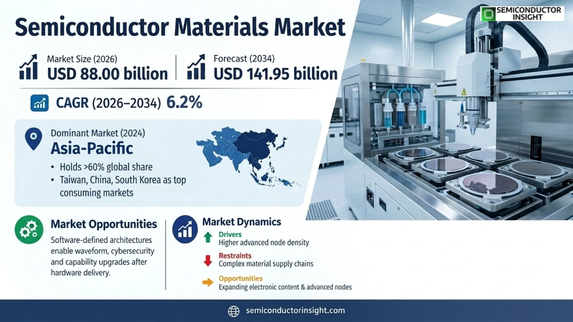
- The source-page CAGR does not reconcile with its market-size anchors. USD 78.09 billion in 2024 and USD 125.96 billion in 2032 imply approximately 6.2% annual growth, not 7.2%, producing rebased values of about USD 82.90 billion in 2025 and USD 141.95 billion in 2034.
Semiconductor Materials Market Overview
Semiconductor Materials Market is valued at USD 82.90 billion in 2025, increases to an estimated USD 88.00 billion in 2026, and is projected to reach USD 141.95 billion by 2034. The selected source-page size anchors imply a 6.2% CAGR during 2026–2034. Asia Pacific is the largest market in 2025 because the source page states that Asia Pacific holds more than 60% share and its FAQ separately identifies Asia as the dominant region, while current demand is being reshaped by advanced-node process complexity, HBM and AI computing, higher lithography intensity, 300 mm wafer demand, advanced packaging, SiC/GaN power devices, localization of high-purity chemicals and new investments in photoresists, electronic gases and packaging materials.
Semiconductor materials include the highly engineered substrates, patterning chemicals, process gases, metals, dielectrics and packaging inputs consumed from wafer preparation through final encapsulation and interconnection. The source page divides the market into wafer fab materials and packaging materials, reflecting two distinct economic stages: front-end materials directly influence transistor formation and yield, while packaging materials protect the die and enable electrical, mechanical and thermal connections in increasingly complex multi-chip systems.
Current industry evidence confirms that material consumption is rising with process intensity. SEMI reported that its independently tracked semiconductor materials market reached USD 73.2 billion in 2025, with wafer-fab materials at USD 45.8 billion and packaging materials at USD 27.4 billion. That external benchmark is lower than the source-page anchor-derived 2025 series and is therefore used only as independent context for category mix, growth and regional direction; the report’s forecast arithmetic continues to follow the source-page USD 78.09 billion 2024 and USD 125.96 billion 2032 anchors.
Materials demand is becoming increasingly strategic because advanced semiconductor manufacturing cannot switch suppliers quickly. Photoresists, gases, wafers, CMP slurries, targets and packaging compounds are qualified against specific process nodes and tool conditions, and trace impurities can alter yield. That makes supply-chain localization and customer co-development critical. TOK, Resonac, Merck and Entegris are expanding materials infrastructure, while advanced packaging consortia are bringing chemical, substrate and equipment companies closer to fabless and semiconductor customers.
Segment Analysis: By Type
The source page segments the market into Wafer Fab Materials and Packaging Materials. Wafer Fab Materials are identified as the technology frontier because advanced-node process steps consume ultra-high-purity wafers, photoresists, gases, wet chemicals, targets and CMP materials, while Packaging Materials are growing with chiplets, HBM, fan-out and 2.5D/3D architectures that require advanced substrates, bonding, molding and thermal materials.
| Type | Technical / commercial role | Market position |
|---|---|---|
| Wafer Fab Materials | Wafer fab materials include silicon wafers, photomasks, photoresists and ancillaries, electronic gases, wet chemicals, sputtering targets and CMP pads/slurries. These products directly interact with wafer surfaces during lithography, deposition, etch, cleaning and planarization. Product qualification centers on purity, uniformity, defectivity and compatibility with a specific process sequence. | Leading source-page type. SEMI independently reported USD 45.8 billion of 2025 wafer-fab-material revenue, up 5.4%, with strong double-digit growth in lithography-related materials and wet chemicals. Advanced logic, HBM and 3D NAND increase steps per wafer and value per wafer even when unit growth is moderate. |
| Packaging Materials | Packaging materials include IC substrates, lead frames, bonding wires, die attach, molding compounds, encapsulants, ceramic packages, underfills, conductive pastes and related interconnect materials. Advanced packaging increases the number of material interfaces and raises thermal, warpage, reliability and fine-line requirements as multiple dies are assembled into one system. | Fast-growing source-page category. SEMI reported independently tracked packaging-material revenue of USD 27.4 billion in 2025, up 9.3%, led by substrates and bonding wire. AI accelerators and HBM push the segment toward higher-density substrates, advanced molding, thermal materials and finer interconnects. |
Secondary segmentation: By Material Technology
The source page further divides the market into Silicon-based, Compound Semiconductors and Emerging Materials. Silicon remains the dominant platform because the entire IC manufacturing ecosystem is built around it, while SiC and GaN are gaining share in high-voltage and high-frequency power applications and 2D or quantum materials remain earlier-stage opportunities.
| Material technology | Commercial implication |
|---|---|
| Silicon-based | Silicon wafers remain the foundational substrate for logic, memory, analog and many power devices. SEMI reported 12,973 million square inches of silicon wafer shipments in 2025, up 5.8%, with AI-driven advanced epitaxial and HBM-related polished wafer demand supporting recovery. Silicon also anchors process chemicals and photoresists optimized around mature and advanced CMOS. |
| Compound Semiconductors | SiC and GaN enable higher voltage, temperature and switching frequency than silicon in selected power and RF applications. Growth creates demand not only for substrates but also for epitaxy, photoresists, implant/etch chemicals and specialized packaging. Material handling and defect control remain more challenging than established silicon manufacturing. |
| Emerging Materials | Emerging materials include 2D semiconductors, advanced dielectrics, novel metals and quantum-material systems being explored for future logic, memory and sensors. Commercial contribution remains limited, but suppliers that develop scalable deposition, cleaning and integration methods can influence the next semiconductor process platform. |
Secondary segmentation: By End User
The source page identifies IDMs, Foundries and OSATs. Foundries are described as transforming material requirements through node specialization and supplier co-development, while IDMs remain major consumers across memory, logic, analog and power. OSATs increasingly influence packaging-material demand because advanced assembly creates more process steps after wafer fabrication.
| End user | Demand characteristics |
|---|---|
| IDMs | Integrated device manufacturers qualify materials across internal wafer and package flows and may maintain unique process recipes for many years. Memory IDMs are important to high-purity wafers, gases, CMP and packaging materials because HBM and advanced DRAM require both front-end scaling and sophisticated stacking. |
| Foundries | Foundries serve many fabless customers and therefore place extreme emphasis on stable yield, process control and change management. Leading nodes require customized resist, precursor and clean-chemical solutions, creating long co-development cycles and high switching costs for qualified suppliers. |
| OSATs | Outsourced assembly and test providers consume substrates, molding compounds, underfills, bonding materials, thermal interfaces and plating chemicals. Chiplets and heterogeneous integration expand the material bill per package and make warpage, thermal conductivity and fine-line performance key purchasing criteria. |
Secondary segmentation: By Manufacturing Stage
The source page splits materials into Front-end Materials, Back-end Materials and Interconnect Materials. Front-end materials are identified as the most rapidly evolving because purity and atomic-scale uniformity directly affect transistor performance and yield, while back-end and interconnect materials gain strategic importance as advanced packaging adds more layers and die interfaces.
| Manufacturing stage | Commercial role |
|---|---|
| Front-end Materials | Wafers, photoresists, gases, chemicals, targets, precursors and CMP materials support transistor formation. Requirements tighten as dimensions shrink and process stacks become more complex. Advanced nodes consume more lithography, deposition, clean and planarization steps, increasing materials intensity per wafer. |
| Back-end Materials | Molding compounds, die attach, underfills and packaging ceramics protect devices and manage mechanical or thermal stress. Advanced packages require lower warpage, high thermal conductivity and compatibility with fine-pitch interconnects, pushing material development beyond traditional commodity encapsulation. |
| Interconnect Materials | Copper, bonding wire, substrates, solder, plating chemistry and redistribution-layer dielectrics form electrical paths between dies and packages. Chiplets and HBM increase interconnect density, making conductor resistance, adhesion, electromigration and fine-line processing important differentiators. |
Segment Analysis: By Application
By application, the source page segments demand into Memory, Logic/MPU, Analog, Discrete Device & Sensor and Others. Memory remains the largest broad consumption category, but Logic/MPU drives the most aggressive material innovation because EUV, advanced deposition and ultra-high-purity chemistry must meet the requirements of leading-edge transistors and AI processors.
| Application | Demand characteristics |
|---|---|
| Memory | DRAM, HBM and 3D NAND consume large volumes of silicon wafers, deposition precursors, etch gases, CMP materials and photoresists. HBM adds advanced packaging substrates, molding and interconnect materials after front-end fabrication. SEMI attributed 2025 wafer-material recovery partly to polished wafers used for HBM and advanced memory. |
| Logic/MPU | Leading logic uses EUV and complex deposition/etch stacks that demand photoresists, masks, specialty gases and atomic-layer precursors with extremely low contamination. The source page identifies Logic/MPU as the innovation driver because material bottlenecks can constrain entire advanced-node process ramps. |
| Analog | Analog devices use mature and specialty process technologies, including high-voltage implants, thick metals, isolation and unique dielectrics. Materials volumes grow with automotive and industrial demand, and long product lifecycles make consistency and change control more important than absolute minimum feature size. |
| Discrete Device & Sensor | Power semiconductors, MEMS and sensors use silicon, SiC, GaN, specialty gases, metals and packaging materials. Automotive electrification and industrial sensing support this segment, while compound-semiconductor devices require specialized substrates and process chemistries. |
| Others | Other applications include RF, photonics, quantum devices and emerging semiconductor architectures. Volumes are smaller but can require premium materials such as high-purity III-V substrates, specialized polymers or novel thin films, creating attractive niches for advanced materials suppliers. |
Regional Analysis
The source page says Asia Pacific holds more than 60% of global semiconductor materials share and its FAQ identifies Asia as the dominant market, with China at USD 11.93 billion in 2024. Independent SEMI 2025 regional tracking also places Taiwan, China and South Korea as the three largest semiconductor-material consuming markets, reinforcing the region’s leadership despite differences in total-market methodology.
Why is semiconductor-material demand so concentrated in Asia Pacific?
Semiconductor materials must be delivered close to fabs with strict purity, shelf-life and change-control requirements. Taiwan, South Korea, China and Japan combine leading foundries, memory IDMs, packaging plants and major suppliers, allowing dense local logistics and rapid technical support. North America is expanding domestic materials and advanced-packaging capability, Europe specializes in wafers, chemicals and power/automotive materials, while South America and MEA remain smaller and import dependent.
| Region | Position | Growth outlook | Demand profile | What decides supplier selection |
|---|---|---|---|---|
| Asia Pacific | Largest – >60% source-page share | High | Foundry, memory and packaging-led | Purity, local supply, qualification and scale |
| North America | Strategic localization market | High | Advanced logic, AI, materials R&D and fab expansion-led | Domestic supply, high-purity capability and customer support |
| Europe | Specialty materials stronghold | Moderate to high | Wafers, chemicals, automotive and power-led | Technology depth, sustainability and reliability |
| South America | Small | Low to moderate | Packaging and basic chemical demand-led | Imports, cost and local processing |
| Middle East & Africa | Emerging | Low from small base | Specialty gas, mining and future fab initiatives-led | Project scale, purification and technology transfer |
Competitive Landscape
The source page formally profiles fifteen companies spanning silicon wafers, photoresists, electronic materials, substrates and advanced packaging: Shin-Etsu Chemical, SUMCO, GlobalWafers, Kyocera, Resonac, SK Siltron, Siltronic, Merck, Entegris, JSR, DuPont, TOK, NSIG, ASE Material and Shinko Electric. The list reflects the market’s broad material scope rather than one product category, so competitive leadership is segmented by wafers, chemicals, resists and packaging technologies.
Shin-Etsu Chemical, SUMCO, GlobalWafers, SK Siltron and Siltronic compete in semiconductor wafers, where crystal quality, diameter, epitaxy and long-term supply agreements determine position. The source page states Shin-Etsu and SUMCO control nearly 60% of silicon wafer supply, although that exact share is treated as source-page evidence rather than independently recalculated here.
Resonac, Merck, Entegris, JSR, DuPont and TOK compete across photoresists, gases, precursors, filtration, CMP and other high-purity process materials. Current 2026 investments show strong demand for lithography and clean chemistry: TOK is adding high-purity chemical capacity and photoresist land, while Resonac is duplicating high-purity HF gas production for advanced etch.
Kyocera, ASE Material and Shinko Electric are more exposed to substrates and packaging materials, where advanced package density, warpage and thermal performance create different technical barriers than front-end chemistry. National Silicon Industry Group represents China’s localization push in large-diameter wafers and related materials, adding a regional strategic dimension to supplier competition.
| Competitive tier | Companies | Why they matter |
|---|---|---|
| Silicon wafer leaders | Shin-Etsu Chemical; SUMCO; GlobalWafers; SK Siltron; Siltronic AG; National Silicon Industry Group (NSIG) | These companies compete on crystal quality, 300 mm scale, epitaxy and long-term fab relationships. AI and HBM raise demand for advanced polished and epitaxial wafers, while localization policies encourage additional regional capacity. |
| Advanced chemical / resist leaders | Resonac Corporation; Merck KGaA; Entegris; JSR Corporation; DuPont; TOKYO OHKA KOGYO CO., LTD. | These suppliers provide photoresists, gases, filtration, deposition materials, CMP and specialty chemicals. Competitive advantage comes from ultra-high purity, process integration and the ability to scale a qualified formulation globally. |
| Packaging and substrate specialists | Kyocera; ASE Material; Shinko Electric Industries | These companies serve ceramic, substrate and advanced package material requirements where electrical routing, thermal management and mechanical warpage determine performance. AI and chiplet packages are increasing technical complexity and value per package. |
Companies profiled in the report
The source page profiles Shin-Etsu Chemical; SUMCO; GlobalWafers; Kyocera; Resonac Corporation; SK Siltron; Siltronic AG; Merck KGaA; Entegris; JSR Corporation; DuPont; TOKYO OHKA KOGYO CO., LTD.; National Silicon Industry Group (NSIG); ASE Material; and Shinko Electric Industries.
Production Capacity Analysis
Semiconductor-material capacity is highly product specific. Silicon wafers require crystal pulling, slicing, polishing and epitaxy; photoresists and chemicals require synthesis, purification and ultra-clean filling; electronic gases require purification and specialized logistics; packaging materials require precision substrate, metal, polymer and ceramic processing. Effective capacity exists only after a manufacturing site and product are qualified by the customer for a specific semiconductor process.
Silicon wafer capacity is measured in usable area and product mix rather than wafer count alone. SEMI reported Q2 2026 shipments of 3,573 million square inches, up 7.4% year over year and 9.1% quarter over quarter. Advanced logic, HBM, power and photonics support demand, but polished, epitaxial and specialty wafers have different manufacturing constraints and selling prices.
High-purity chemical capacity is expanding in Japan. TOK began operations at its Aso Kumamoto site with about ¥13 billion of investment for high-purity chemical supply and quality control, while Resonac is establishing a two-site domestic high-purity HF gas production system. These projects show that supply resilience is being built at the material-specific process level rather than through generic chemical expansion.
Photoresist and packaging capacity also depends on development infrastructure. TOK’s 90,794-square-meter Koriyama land acquisition sits next to an existing photoresist/high-purity chemical plant, while the US-JOINT Silicon Valley center provides cleanrooms and packaging process equipment for material validation. R&D, qualification and local technical support are therefore part of effective capacity.
Market Dynamics
Market growth is driven by increasing process steps, AI/HBM, advanced packaging, wafer recovery and power-semiconductor materials, while restraints include extreme purity requirements, environmental regulation, geographic concentration and long qualification cycles. Semiconductor materials do not behave like commodity chemicals because small formulation or contamination changes can alter wafer yield across billions of dollars of downstream equipment and chip output.
Market Drivers
| Driver | Directional impact* | Commercial mechanism |
|---|---|---|
| Advanced-node process intensity | High | More lithography, deposition, etch and CMP steps increase material consumption per wafer and require tighter purity at leading nodes. |
| AI & HBM manufacturing | High | Advanced logic and memory raise wafer, photoresist, gas, CMP and packaging-material demand simultaneously. |
| Advanced packaging | High | Chiplets and HBM require substrates, molding, underfill, bonding and redistribution materials with higher density and thermal performance. |
| SiC/GaN power electronics | Medium to High | EV and energy applications expand specialty substrate, epitaxy, resist, etch and packaging material requirements. |
Process complexity raises materials intensity per wafer
Leading-edge semiconductor manufacturing uses more masking, deposition, clean, etch and planarization steps than mature nodes. Even if wafer starts grow slowly, the material value consumed per advanced wafer can increase because each step requires precise chemicals, gases and films. This supports structural growth for high-purity suppliers rather than purely cyclical volume expansion.
AI and HBM pull multiple material categories together
AI logic needs advanced lithography and deposition, HBM requires high-quality wafers and complex memory processing, and the final package needs advanced substrates, bonding and thermal materials. SEMI’s 2025 data showed growth in both wafer fab and packaging materials, demonstrating how one compute trend propagates across the material stack.
Advanced packaging shifts value toward backend materials
Chiplets and heterogeneous integration add fine-pitch substrates, underfills, mold compounds, plating and redistribution-layer materials after the wafer is fabricated. Packaging-material revenue grew faster than wafer-fab materials in SEMI’s 2025 benchmark, reflecting the increasing amount of material engineering required outside front-end transistor formation.
Power electronics expand compound-semiconductor materials
SiC and GaN devices are used in EV traction, fast charging and high-efficiency power systems. Their substrates, epitaxial layers and process chemistries differ from mainstream silicon, creating opportunities for material suppliers that can meet defect, thermal and high-voltage requirements at commercial yield.
Market Restraints
| Restraint | Directional impact* | Commercial mechanism |
|---|---|---|
| Ultra-high purity requirements | High | Trace particles, metals or moisture can destroy wafer yield, making purification, logistics and analytical control expensive. |
| Long customer qualification | High | A new material or manufacturing site may require months or years of process and reliability validation before revenue scales. |
| Environmental regulation | Medium to High | PFAS, greenhouse gases and hazardous chemicals face tightening rules that can force process redesign and requalification. |
| Geographic concentration | Medium to High | Many critical wafers, photoresists and chemicals are concentrated in Japan, Korea and Taiwan, creating resilience concerns. |
Purity requirements create high fixed cost and barriers to entry
Semiconductor-grade materials often require contamination limits far tighter than ordinary industrial chemicals. Suppliers need dedicated production, filtration, analytical labs, clean containers and controlled logistics. This capital and know-how burden makes it difficult for regional chemical companies to enter advanced-node supply simply by upgrading a conventional plant.
Qualification makes capacity slow to become saleable
A customer does not buy a semiconductor material because the supplier can produce it; the exact product and manufacturing site must be qualified in a process flow. Changes can alter yield, film thickness, etch rate or package reliability. This means announced capacity can sit below full utilization while customer approval progresses.
Environmental rules can force expensive reformulation
PFAS, perfluorocarbon gases, solvents and hazardous precursors face growing regulatory scrutiny. Lower-impact alternatives can create opportunity, but any change must maintain process performance and often triggers customer requalification. Compliance therefore adds cost and development risk rather than simply removing old materials.
Regional concentration remains a resilience risk
Japan and other Asian markets dominate several wafer, resist and chemical categories. New capacity in the United States, Europe and China is improving diversification, but reproducing supplier ecosystems, specialized equipment and customer qualification takes years. Geopolitical or disaster risk therefore remains structurally important.
Market Opportunities
High-NA EUV and next-generation resists
Leading logic requires new resist platforms that balance resolution, sensitivity and defectivity. TOK’s 2026 investment in molecular-resist development and ongoing capacity expansion show that EUV remains a high-value innovation area inside the broader materials market.
High-purity electronic gases
Resonac’s second Japanese high-purity HF site reflects growing demand for etch gases in advanced processes, including cryogenic etching. Additional regional gas production can improve resilience and shorten logistics for materials that require specialized cylinders and strict purity control.
Advanced packaging co-development
US-JOINT provides a shared R&D environment for patterning, bonding, molding and plating. Material companies can shorten commercialization cycles by testing new formulations directly with packaging equipment and semiconductor users, creating opportunities beyond traditional standalone material qualification.
Localized semiconductor-material ecosystems
New fabs in the United States, Europe and Asia create demand for nearby high-purity chemicals, filtration and wafer support. Suppliers can localize final purification, filling or service close to customers even when upstream synthesis remains centralized, improving resilience without duplicating the entire value chain.
Supply Chain Analysis
Raw feedstocks & high-purity precursors
Crystal growth / synthesis / purification
Formulation, finishing & clean packaging
Fab / OSAT qualification and recurring consumption
Raw feedstocks & high-purity precursors
Semiconductor materials start with polysilicon, quartz, metals, gases, monomers, solvents and specialty chemicals. Upstream purity and traceability determine how difficult later purification will be, making secure feedstock relationships strategically important.
Crystal growth / synthesis / purification
Wafer suppliers grow and process crystals, while chemical and gas suppliers synthesize and purify materials to semiconductor-grade specifications. Process know-how, analytical control and contamination management form the core intellectual property of many materials businesses.
Formulation, finishing & clean packaging
Photoresists, slurries, chemicals and packaging compounds are blended, filtered and filled in ultra-clean environments. Wafers are polished or epitaxially finished and packed in contamination-controlled carriers. Site-specific qualification often applies to this finishing step.
Fab / OSAT qualification and recurring consumption
Customers qualify materials on specific process nodes, tools and packages and then consume them repeatedly in high-volume production. Strong technical support and stable lot-to-lot performance create long supplier relationships and high switching costs.
Recent Developments
Recent primary-source developments show the semiconductor-material ecosystem investing simultaneously in silicon-wafer supply, high-purity gases and chemicals, packaging R&D and regional resilience. The independent SEMI market benchmark differs numerically from the source-page forecast series, so its 2025 figures are used as external industry context rather than to replace the source anchors.
July 29, 2026 – SEMI reported Q2 silicon wafer shipments up 7.4% year over year
SEMI’s Silicon Manufacturers Group reported worldwide Q2 2026 silicon wafer shipments of 3,573 million square inches, up 7.4% from Q2 2025 and 9.1% from Q1 2026. The group cited strong AI-related demand extending from advanced logic and memory into power devices and photonics, alongside recovering industrial and automotive markets.
June 25, 2026 – Resonac announced a two-site high-purity HF gas production system
Resonac said it will start high-purity hydrogen fluoride gas production at its Tokuyama Plant during 2026, adding to existing Kawasaki output. The company linked demand to advanced semiconductor etching, including cryogenic etch, and said the two-site system is intended to strengthen stable supply.
June 8, 2026 – TOK began operations at the Aso Kumamoto high-purity chemical site
TOK announced operation of its Aso Kumamoto site for high-purity chemical supply and quality control. The 128,000-square-meter site represents approximately ¥13 billion of investment and forms part of TOK’s record ¥76 billion three-year capital plan to expand semiconductor production capacity in Japan and overseas.
May 12, 2026 – SEMI reported record 2025 semiconductor-material revenue
SEMI’s independent MMDS benchmark reported USD 73.2 billion of semiconductor-material revenue in 2025, up 6.8%, with wafer fab materials at USD 45.8 billion and packaging materials at USD 27.4 billion. Taiwan, China and South Korea were the three largest tracked consuming markets.
April 21, 2026 – US-JOINT launched a Silicon Valley advanced-packaging R&D center
TOK announced full-scale operation of US-JOINT, a twelve-company consortium with cleanrooms and equipment for patterning, bonding, molding, plating, evaluation and analysis. The center allows material and equipment suppliers to validate advanced packaging concepts with fabless and semiconductor users in the United States.
March 25, 2026 – TOK acquired 90,794 square meters for future Koriyama expansion
TOK acquired a roughly 90,794-square-meter industrial site in Koriyama, Japan, for approximately ¥1.5 billion. The site is near an existing plant that manufactures photoresist and high-purity chemicals and is intended to secure space for future semiconductor-market growth.
Report Scope & Segmentation
| Attribute | Coverage |
|---|---|
| Market | Semiconductor Materials |
| Base Year | 2025 |
| Estimated Year | 2026 |
| Forecast Period | 2026–2034 |
| 2025 Market Size | USD 82.90 billion |
| 2034 Forecast Size | USD 141.95 billion |
| CAGR | 6.2% (2026–2034) |
| Largest Market in 2025 | Asia Pacific |
| By Type | Wafer Fab Materials; Packaging Materials |
| By Application | Memory; Logic/MPU; Analog; Discrete Device & Sensor; Others |
| By End User | IDMs (Integrated Device Manufacturers); Foundries; OSAT (Outsourced Assembly and Test) |
| By Material Technology | Silicon-based; Compound Semiconductors; Emerging Materials |
| By Manufacturing Stage | Front-end Materials; Back-end Materials; Interconnect Materials |
| Regions | Asia Pacific; North America; Europe; South America; Middle East & Africa |
| Companies Profiled | Shin-Etsu Chemical; SUMCO; GlobalWafers; Kyocera; Resonac Corporation; SK Siltron; Siltronic AG; Merck KGaA; Entegris; JSR Corporation; DuPont; TOKYO OHKA KOGYO CO., LTD.; National Silicon Industry Group (NSIG); ASE Material; Shinko Electric Industries |
Frequently Asked Questions
What is the Semiconductor Materials market size in 2025?
The source page publishes USD 78.09 billion in 2024 and USD 125.96 billion in 2032. Those anchors imply a 2025 market size of approximately USD 82.90 billion. Applying the same compound factor gives an estimated USD 88.00 billion in 2026 and approximately USD 141.95 billion in 2034.
What is the projected market size by 2034?
The rebased 2034 Semiconductor Materials market is approximately USD 141.95 billion. This extends the source page’s 2024–2032 market-size anchors using the same compound annual relationship and keeps the 2025 base, 2026 estimate and 2034 endpoint mathematically consistent.
Why is the CAGR 6.2% instead of the page’s 7.2%?
USD 78.09 billion in 2024 and USD 125.96 billion in 2032 imply approximately 6.16% compound annual growth over eight years, not 7.2%. Under the batch methodology, the source-page market-size anchors control when the printed CAGR does not reconcile.
Which material type leads the market?
Wafer Fab Materials lead the source-page type segmentation and include silicon wafers, photomasks, photoresists, wet chemicals, gases, sputtering targets and CMP materials. Packaging Materials include substrates, lead frames, bonding wire, ceramics and molding compounds and are growing rapidly with advanced packaging.
Which application is the largest?
The source page states that Memory continues to dominate wafer-fab material consumption, while Logic/MPU drives the most aggressive innovation because leading nodes require extreme purity, EUV lithography and atomic-level deposition or etch control.
Which region dominates the market?
Asia Pacific is the dominant region. The source page states the region holds more than 60% share and separately says China reached USD 11.93 billion in 2024. Independent SEMI tracking also ranks Taiwan, China and South Korea as the three largest semiconductor-material consuming markets in 2025.
Why does SEMI report a different 2025 market total?
SEMI’s independent MMDS benchmark reported USD 73.2 billion in 2025, while the source-page anchor series implies about USD 82.9 billion. Because the user workflow requires source-page anchors to control the forecast series, the SEMI figure is used only as external context for segment growth and regional direction rather than replacing the source data.
How is AI changing semiconductor-material demand?
AI increases leading-logic, HBM and advanced-packaging demand simultaneously. More wafer process steps raise photoresist, gas, chemical and CMP consumption, while HBM and chiplet packaging increase substrates, molding, bonding and thermal-material requirements. Current wafer shipment and supplier-capacity investments confirm this broader materials intensity.
Who are the companies profiled in the source report?
The source page profiles Shin-Etsu Chemical, SUMCO, GlobalWafers, Kyocera, Resonac, SK Siltron, Siltronic, Merck, Entegris, JSR, DuPont, TOK, National Silicon Industry Group, ASE Material and Shinko Electric Industries.
What is the main strategic risk through 2034?
The main risk is that regional capacity or new suppliers cannot achieve customer-qualified purity and yield fast enough. Semiconductor materials require exact process compatibility and long validation cycles, so supply-chain diversification takes years even when governments or companies commit significant capital.

Get Sample Report PDF for Exclusive Insights
Report Sample Includes
- Table of Contents
- List of Tables & Figures
- Charts, Research Methodology, and more...
 Download Sample Report PDF





