
Key Statistics
Key Takeaways
- FFKM seals are the value-leading material class because the most aggressive plasma, deposition and high-temperature process steps reward longer seal life, lower contamination and reduced maintenance frequency rather than the lowest unit price.
- Dry/wet etching and plasma systems remain the most demanding application cluster, where fluorine- and chlorine-rich chemistries, vacuum duty and particle control make seal material selection directly relevant to tool uptime and wafer yield.
- Asia Pacific is the largest regional market because Taiwan, South Korea, China and Japan concentrate wafer-fabrication capacity, while supplier localization around major fab clusters shortens qualification support and replenishment lead times.
- Cleanroom manufacturing and material qualification are stronger competitive barriers than molding capacity alone. The commercial advantage lies in repeatable purity, trace-metal control, low outgassing and documented performance across specific process chemistries.
- Fab and equipment investment remains the central demand engine. SEMI projected global semiconductor equipment sales of USD 125.5 billion in 2025 and USD 138.1 billion in 2026, expanding the installed base of chambers, valves, vacuum lines and wet-process systems that consume high-performance seals.
Sealing Products in Semiconductor Market Overview
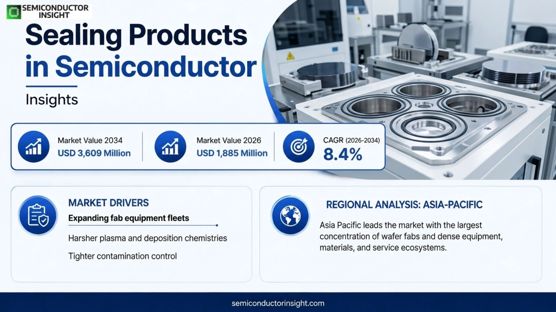
Sealing Products in Semiconductor Market is estimated at USD 1,753 million in 2025 and is projected to reach USD 3,609 million by 2034, representing a CAGR of 8.4% during 2026–2034. Asia Pacific is the largest regional market because the highest concentration of front-end wafer fabrication and advanced memory production sits in Taiwan, South Korea, China and Japan.
Semiconductor sealing products are engineered O-rings, gaskets, valve-door seals, diaphragms and custom polymer or polymer-metal assemblies used to preserve vacuum integrity, isolate aggressive chemicals and prevent contamination inside wafer-fabrication and sub-fab equipment. The market is distinguished from general industrial sealing by the requirement to combine chemical resistance, thermal stability, exceptionally low extractables and outgassing, predictable compression behavior and cleanroom-controlled manufacturing in applications where a microscopic particle or trace contaminant can create a yield-loss event.
The commercial value of a semiconductor seal is therefore measured through tool uptime and process stability rather than through component cost alone. DuPont documents Kalrez perfluoroelastomer parts across etch, deposition, ash/strip and wet processes, while Trelleborg manufactures semiconductor products in controlled cleanroom environments and positions high-purity FFKM and FKM materials around reduced particle generation, lower outgassing and longer maintenance cycles. These requirements make application engineering, compound formulation and qualification history core components of supplier value.
Industry capacity expansion provides the demand backdrop. SEMI forecast worldwide semiconductor manufacturing equipment sales at USD 125.5 billion in 2025 and USD 138.1 billion in 2026, while its October 2025 outlook put 300 mm fab equipment spending at USD 374 billion over 2026–2028. Every additional deposition, etch, clean, thermal and vacuum tool creates multiple sealing locations, while higher process intensity at leading nodes increases replacement demand per installed tool by exposing seals to more aggressive chemistries and longer duty cycles.
Segment Analysis: By Type
By type, the market is segmented into FFKM, FKM, PTFE, EPDM and VMQ. FFKM is the value-leading class in the most demanding plasma and deposition environments because its chemical and thermal resistance supports longer maintenance intervals, while FKM retains substantial volume where process conditions permit a lower-cost elastomer without compromising contamination control.
| Type | Technical role | Market position |
|---|---|---|
| FFKM | Perfluoroelastomer sealing for aggressive plasma, high-temperature and chemically severe process environments. | Largest value segment. Its premium is supported by lower particle generation, better chemical resistance and extended service intervals in etch, CVD, ALD, ash/strip and high-vacuum service. |
| FKM | Fluoroelastomer seals for moderately aggressive chemistries and temperature ranges. | High-volume value alternative where FFKM performance is unnecessary. Qualification and contamination specifications still differentiate semiconductor grades from general industrial FKM. |
| PTFE | Fluoropolymer seals and spring-energized designs used where chemical inertness, low friction and dimensional stability are priorities. | Important in wet processing, chemical delivery, vacuum and dynamic applications. PTFE-based engineered seals compete on geometry and surface finish as much as resin selection. |
| EPDM | Elastomer class with useful resistance to selected aqueous chemistries, steam and polar media. | Selective use in wet and utility-side applications; limited in aggressive fluorine plasma or hydrocarbon-rich environments where fluorinated materials are preferred. |
| VMQ | Silicone elastomer used where flexibility and broad temperature performance matter more than severe plasma resistance. | Niche semiconductor use in non-critical or lower-chemical-exposure locations, with demand constrained by contamination and plasma-performance requirements. |
Material economics and qualification depth
Material choice is made against a process-specific failure mode rather than a generic temperature rating. DuPont’s semiconductor selector materials place different Kalrez grades across PECVD, PEALD, conductor etch, dielectric etch and ash/strip, with cited maximum service temperatures extending into roughly 300 °C ranges for several deposition processes. The commercial consequence is a portfolio market: suppliers need multiple compounds, geometries and cleanroom finishing routes so an equipment OEM can qualify a seal at each location without redesigning the surrounding hardware.
Segment Analysis: By Application
By application, the market covers Dry/Wet Etching, Plasma Systems, Chemical Vapor Deposition (CVD), Atomic Layer Deposition (ALD), Physical Vapor Deposition (PVD) and adjacent process steps. Etch and plasma environments represent the strongest value pool because seal failure can simultaneously increase particles, destabilize vacuum and shorten preventive-maintenance intervals.
| Application | Demand characteristics |
|---|---|
| Dry/Wet Etching | Dry etch exposes seals to fluorine- and chlorine-based plasmas, while wet etch and cleaning expose components to acids, bases and oxidizers. Purchasing centers on compatibility with the exact chemistry, particle performance, compression set and the ability to maintain vacuum or liquid containment through repeated thermal cycles. |
| Plasma Systems | Plasma ash, strip and clean systems create severe ion, radical and thermal exposure. High-purity FFKM grades earn a premium where lower erosion and particle shedding extend chamber maintenance intervals and reduce defect risk. |
| Chemical Vapor Deposition (CVD) | CVD tools combine precursor exposure, elevated temperature and plasma-based chamber cleaning. Seals are specified at chamber lids, valves, gas delivery and exhaust locations, so a supplier must manage both chemical resistance and low outgassing. |
| Atomic Layer Deposition (ALD) | ALD and PEALD demand precise, repeated precursor pulses and increasingly high-temperature operation. Seal stability matters because small changes in chamber integrity or contamination can undermine thickness uniformity and film quality over long production runs. |
| Physical Vapor Deposition (PVD) | PVD sealing emphasizes high vacuum, particle control and resistance to process by-products. Dynamic and gate-valve locations can require engineered geometries or bonded seals that combine elastomer purity with metal support structures. |
Regional Analysis
Asia Pacific leads the semiconductor sealing-products market because it combines the largest concentration of wafer fabs with dense equipment, materials and service ecosystems. North America remains disproportionately important in material formulation and equipment-OEM qualification, while Europe combines precision sealing engineering with lithography and vacuum-system demand.
How does regional demand differ across the semiconductor sealing-products market?
Regional demand is shaped by where wafer-processing tools are installed and where sealing materials are qualified. Asia Pacific is the volume center because fabs in Taiwan, South Korea, China and Japan operate large fleets of etch, deposition and cleaning equipment. North America is qualification-intensive because major equipment makers and specialty-material suppliers influence global specifications. Europe combines leading lithography, vacuum and specialty-material capability. South America and Middle East & Africa remain smaller, project-led markets tied to emerging semiconductor, electronics and research investments.
| Region | Position | Growth outlook | Demand profile | What decides supplier selection |
|---|---|---|---|---|
| Asia Pacific | Largest | Highest absolute expansion | Fab-density and localization led | Cleanroom purity, local technical support, tool qualification and delivery reliability |
| North America | Second tier by demand; technology-critical | Strong | Equipment-OEM and advanced-node led | Qualification history, compound IP, documentation and field performance |
| Europe | Strategic specialty market | Moderate to strong | Lithography, vacuum and precision engineering led | Purity, environmental compliance, engineering support and traceability |
| South America | Small base | Selective | Import and industrial-electronics led | Landed cost, distributor availability and application support |
| Middle East & Africa | Emerging | Project-led | New semiconductor initiatives and research led | Supply assurance, qualification support and local inventory |
Competitive Landscape
Competition is organized around material formulation, process qualification, cleanroom manufacturing and application engineering. The strongest suppliers are not simply seal manufacturers; they maintain semiconductor-specific compounds, controlled production environments, failure-analysis capability and long-lived relationships with equipment OEMs and fabs.
At the premium end, perfluoroelastomer formulations create differentiated performance in plasma, deposition and thermal processes. DuPont positions Kalrez around semiconductor-specific compounds and process selectors, while Trelleborg markets Isolast PureFab FFKM and Resifluor PureFab FKM grades alongside cleanroom production, micromolding and custom engineering. These portfolios compete on the ability to solve a known chamber failure mechanism-particle shedding, compression set, chemical attack, permeation or outgassing-rather than on catalogue breadth alone.
Japanese suppliers such as NOK, Eagle Industry and VALQUA bring deep relationships with domestic equipment and materials ecosystems, while Parker Hannifin, Freudenberg, Saint-Gobain, Greene Tweed and Precision Polymer Engineering contribute broad polymer, PTFE and engineered-seal expertise. Regional specialists compete effectively where they can shorten delivery times or customize geometries, but entering a critical chamber location remains difficult because changing a seal can require months of testing and documentation before a fab accepts the new material.
Cleanroom capacity has become a visible strategic asset. Trelleborg cites ISO Class 7 manufacturing and ISO Class 5 washing/packing capabilities, while its Malta expansion adds semiconductor-focused FKM and FFKM cleanroom space. This shifts competition toward vertically controlled compounding, molding, post-cure, cleaning, inspection and packaging, because contamination introduced at any stage can negate the chemical advantages of an otherwise superior compound.
Key Industry Players
- DuPont de Nemours, Inc.
- NOK CORPORATION
- Eagle Industry Co., Ltd.
- Parker Hannifin Corporation
- Daikin Industries, Ltd.
- VALQUA, Ltd.
- Trelleborg Sealing Solutions
- Applied Seals North America
- Saint-Gobain Performance Plastics
- Precision Polymer Engineering (IDEX Corporation)
- MNE Co., Ltd.
- Freudenberg Sealing Technologies
- Greene Tweed & Co.
- Vulcan Seals Inc.
- Maxmold Polymer Technology Co., Ltd.
Competitive capability map
| Competitive capability | Why it matters | Supplier implication |
|---|---|---|
| Semiconductor-specific compound portfolio | Etch, deposition, wet clean and thermal locations impose different chemical and temperature requirements. | Suppliers with multiple FFKM, FKM and PTFE formulations can optimize total cost of ownership instead of forcing one compound across every seal location. |
| Cleanroom processing | Trace particles, metals, extractables and packaging contamination can become yield risks. | Controlled molding, post-cure, washing and double-bagging strengthen qualification and reduce incoming-cleanliness burden for fabs and OEMs. |
| Application engineering | Seal geometry, compression, groove fill, temperature and plasma exposure determine field life. | FEA, plasma testing, failure analysis and rapid prototyping shorten the route from process problem to qualified replacement. |
| Global service footprint | A qualified tool platform may be installed across Taiwan, Korea, the U.S. and Europe. | Global manufacturing and local stocking improve continuity while preserving the same material specification across fab locations. |
Production Capacity Analysis
Production capacity is constrained less by elastomer tonnage than by the availability of qualified semiconductor-grade compounding, precision molding, post-cure, cleaning, inspection and controlled packaging. The capacity that matters commercially is the capacity to reproduce a validated compound and geometry at contamination levels acceptable to a specific process tool.
FFKM supply is inherently more specialized than general elastomer supply because polymer chemistry, fillers, cure systems and post-processing determine plasma resistance, compression set, trace-metal content and outgassing. Semiconductor suppliers therefore protect compound recipes and tightly control process windows. Increasing output is not equivalent to adding presses: new tooling, cleanroom space, operators, inspection equipment and process validation must be added without changing the material characteristics that customers previously qualified.
Trelleborg’s network illustrates this multi-stage capacity model. Its semiconductor cleanrooms are used from production through washing and packaging, while the Yongin site combines elastomer manufacturing with semiconductor-focused engineering and plasma-lab capabilities. The Malta expansion adds more than 500 square meters of cleanroom space for FKM and FFKM products. These investments expand qualified throughput and regional resilience simultaneously, which is more strategically valuable than low-cost commodity molding capacity.
Upstream concentration in high-performance fluorinated polymers and specialty additives remains a supply-chain risk. Any change in raw material, cure chemistry or manufacturing site can trigger customer change-control requirements. As a result, dual-sourcing and business-continuity planning must preserve equivalence at the compound and finished-seal level, not merely secure a second source of base polymer.
| Capacity layer | Constraint | Market implication |
|---|---|---|
| Compound formulation | Specialty fluoropolymers, fillers, cure systems and proprietary recipes. | Raw-material changes can alter particles, outgassing or compression performance and may require requalification. |
| Precision molding | Tooling accuracy, flash control, large-diameter and custom geometries. | Micromolding, bonded seals and large custom O-rings create higher barriers than standard molded parts. |
| Post-cure and cleaning | Time, temperature, cleanroom capacity and contamination control. | This stage directly affects extractables, outgassing and delivery throughput for semiconductor-grade parts. |
| Inspection and packaging | Defect control, traceability, double bagging and clean handling. | Capacity must scale without increasing particle risk or weakening lot-level documentation. |
Market Dynamics
The market is pulled upward by fab equipment investment and harsher process conditions, but restrained by long qualification cycles, specialty-material cost and the risk that environmental policy changes the accepted fluoropolymer portfolio. Growth therefore favors suppliers that can combine material innovation with conservative change control.
The demand mechanism is unusually recurring. A new fab creates original-equipment demand when process tools are installed, then replacement demand as seals age through plasma exposure, thermal cycling and chemical attack. Advanced nodes increase both the number of process steps and the cost of unscheduled downtime, making maintenance interval and contamination performance more commercially important. The result is a component market whose revenue can grow faster than the installed tool base when process severity and maintenance intensity rise.
At the same time, qualification slows supplier switching. Fabs and equipment OEMs must prove that a new seal does not introduce particles, metals, outgassing, leakage or premature compression loss. A supplier that wins a critical chamber location can therefore retain that position for multiple equipment generations, but a new entrant may need extensive lab and field testing before it generates meaningful production revenue.
Market Drivers
Four forces provide the strongest structural support: expanding fab equipment fleets, more severe plasma and deposition chemistries, tighter contamination control, and the economic value of extending preventive-maintenance intervals.
| Factor | Estimated impact on CAGR forecast* | Commercial mechanism |
|---|---|---|
| Fab and semiconductor-equipment expansion | +2.4 pp | More chambers, valves, vacuum lines and wet-process systems increase the installed population of semiconductor-grade seals. |
| Advanced-node process severity | +1.8 pp | High-aspect-ratio etch, ALD/PEALD and aggressive chamber cleans accelerate adoption of premium FFKM and engineered seals. |
| Yield and contamination control | +1.3 pp | Lower particle and outgassing performance makes seal quality part of wafer-yield protection rather than maintenance cost alone. |
| Maintenance-cycle economics | +0.9 pp | Longer seal life reduces planned and unplanned downtime, supporting premium pricing where tool utilization is high. |
Fab equipment expansion increases the installed sealing base
SEMI forecast semiconductor manufacturing equipment sales of USD 125.5 billion in 2025 and USD 138.1 billion in 2026, while 300 mm fab-equipment investment is expected to total USD 374 billion during 2026–2028. Each process chamber, vacuum line, valve, gas-delivery assembly and chemical-handling subsystem contains sealing locations. The commercial effect is both an original-equipment opportunity and a durable replacement stream after tools enter high-volume production.
Advanced plasma and deposition processes reward premium materials
Leading-edge etch, PECVD, PEALD, ALD and ash/strip processes expose seals to combinations of fluorine, chlorine, oxygen plasma, high temperature and vacuum. DuPont’s semiconductor product guidance maps different Kalrez grades to specific process chemistries and service temperatures, demonstrating why a general-purpose elastomer cannot address the entire fab. As process windows become harsher, the share of value captured by FFKM and custom engineered seals increases.
Contamination control makes seals part of yield management
A seal that sheds particles or releases extractables can create defects well beyond the value of the component itself. Trelleborg manufactures semiconductor products in cleanroom environments and emphasizes high-purity materials, ultra-low trace metals and low outgassing, while DuPont positions purity and reduced particle generation as central performance variables. This makes incoming cleanliness, packaging and lot traceability procurement criteria rather than optional quality features.
Longer maintenance intervals create measurable total-cost benefits
The economic case for premium sealing becomes strongest where a seal replacement requires chamber venting, service labor, requalification and lost wafer output. DuPont documents selected fab evaluations in which Kalrez seals extended preventive-maintenance targets or wafer-cycle life versus incumbent materials. Even when a premium seal costs several times more than a standard elastomer, a meaningful extension in chamber uptime can justify the higher component price.
Market Restraints
Growth is moderated by specialty-material cost, long qualification cycles, raw-material concentration and increasing scrutiny of fluorinated chemistries. These restraints do not eliminate demand, but they influence which materials can scale and how quickly suppliers can win new specifications.
| Factor | Estimated impact on CAGR forecast* | Commercial mechanism |
|---|---|---|
| Long qualification and change-control cycles | -1.3 pp | Testing for contamination, chemical compatibility and lifetime delays supplier conversion even when a new material is technically attractive. |
| High FFKM and specialty-material cost | -0.8 pp | Customers reserve the highest-cost compounds for locations where downtime or contamination economics support the premium. |
| Raw-material and formulation concentration | -0.6 pp | Specialty fluoropolymer supply disruptions can constrain finished-seal output and complicate dual sourcing. |
| PFAS and environmental policy uncertainty | -0.5 pp | Policy pressure encourages alternative materials but can raise R&D, documentation and requalification costs. |
Qualification cycles slow share shifts
A semiconductor seal is often embedded inside a validated process chamber, so changing material may require bench testing, plasma or chemical compatibility work, particle and extractables analysis, and extended field trials. This creates strong switching inertia. Established suppliers benefit from long qualification histories, while new entrants must fund development and application support well before volume revenue appears. The same barrier also slows adoption of otherwise promising new compounds.
Premium materials create selective rather than universal adoption
FFKM delivers exceptional chemical and thermal performance but is materially more expensive than FKM, EPDM or VMQ. Fabs therefore apply premium compounds selectively to failure-critical locations and use lower-cost materials where chemistry and temperature permit. This limits unit-volume penetration even when FFKM captures a disproportionately high share of market value, and it keeps application engineering central to procurement decisions.
Specialty fluoropolymer supply can become a bottleneck
High-performance sealing depends on a narrower upstream base of fluorinated polymers, fillers and cure systems than commodity elastomers. A raw-material change can affect contamination and lifetime performance, meaning a supplier cannot always switch sources without customer notification or requalification. This increases inventory requirements and encourages geographically diversified manufacturing, but it also raises the working capital needed to protect continuity.
Environmental policy increases the cost of material transition
Fluorinated materials are deeply embedded in high-performance semiconductor sealing because few alternatives match their combined plasma, chemical and thermal resistance. At the same time, PFAS policy is driving customers and suppliers to evaluate alternatives. Trelleborg’s 2025 launch of a PFAS-free elastomer for demanding semiconductor applications shows the direction of travel, but broad substitution requires process-by-process proof and can create years of parallel qualification expense.
Market Opportunities
The strongest opportunities are in leading-edge plasma environments, regional cleanroom capacity, custom bonded assemblies and material platforms that reduce fluorinated content without sacrificing uptime.
Leading-edge etch and ALD seal platforms
High-aspect-ratio memory etch, advanced logic patterning, ALD and PEALD place higher demands on plasma resistance, thermal stability and particle performance. Suppliers that can map compounds to exact chemistries and prove longer maintenance intervals can capture premium content per tool. The opportunity is not only selling more O-rings; it is becoming the approved material platform across chamber lids, valves, gas delivery, exhaust and foreline locations.
Regional cleanroom manufacturing beside fab clusters
Fab regionalization is expanding semiconductor production in the United States, Europe, Japan, Korea and Southeast Asia. Local or regional cleanroom production can shorten replenishment lead time, simplify engineering interaction and strengthen business continuity. Trelleborg’s Malta expansion and existing Yongin semiconductor operation illustrate the strategic value of adding controlled manufacturing capacity close to customers rather than relying on one global export base.
Bonded seals and custom assemblies
Equipment makers increasingly seek assemblies that reduce installation variability and combine elastomer, metal and fluoropolymer functions. Bonded slit-valve doors, diaphragms, spring-energized PTFE seals and custom large-diameter rings can capture more value than standard O-rings because geometry and manufacturing know-how become part of the qualification. Suppliers with metal preparation, bonding and precision molding can therefore expand content per subsystem.
PFAS-reduction and alternative material development
Environmental pressure creates a long-term innovation opportunity for materials that reduce or eliminate targeted fluorinated substances while retaining semiconductor-grade purity and lifetime. The winner will not be the first material with a new label; it will be the material that survives plasma, heat and chemical testing without increasing particles or downtime. Suppliers that can support customers through dual-material qualification may gain share as regulations evolve.
Supply Chain Analysis
The supply chain runs from specialty polymer chemistry through compounding, precision molding, cleanroom finishing and finally equipment-OEM or fab qualification. Value capture increases sharply at the later stages because a finished seal must combine material performance with validated geometry, cleanliness and process documentation.
Specialty polymer inputs
The upstream layer determines the theoretical limits of chemical and thermal performance. FFKM and high-purity FKM supply is more concentrated than general elastomer supply, while PTFE performance depends on resin quality, machining or molding route and surface finish. Semiconductor compounders add value by controlling trace metals, fillers and cure chemistry. Any upstream change can propagate into outgassing or particle behavior, making supplier change control commercially important.
Compounding and precision forming
Compound formulation and molding convert raw polymer into a semiconductor-specific seal. Flash control, groove geometry, bonded metal surfaces, dimensional stability and post-cure conditions affect field life. Micromolding and large-diameter custom processes create distinct capabilities, so suppliers can differentiate through manufacturing technology as well as chemistry. This stage also determines how rapidly a new custom design can move from prototype to qualification lot.
Cleanroom finishing and packaging
Semiconductor parts require handling discipline after molding because a clean compound can still be contaminated during inspection, washing or packaging. Trelleborg states that selected semiconductor products are produced in ISO Class 7 environments and washed and double-bagged in ISO Class 5 areas. The commercial implication is that cleanroom space becomes a capacity asset and packaging documentation becomes part of the supplied product.
OEM and fab qualification
The final supply-chain stage creates the strongest customer lock-in. Equipment makers and fabs validate material, geometry and cleanliness in a specific location, then specify that part for production or service. A successful qualification can support demand across a global fleet of identical tools. Conversely, a raw-material or site change may require customer notification, comparative data or renewed testing, which is why business continuity must be engineered into the approved supply route.
Recent Developments
Recent developments show suppliers expanding cleanroom capacity and broadening material portfolios to address both more aggressive process conditions and emerging environmental requirements.
Trelleborg reported that 2025 included the launch of its first PFAS-free elastomer for demanding semiconductor applications and the inauguration of an expanded Malta facility. The combination is strategically important because it addresses two purchasing priorities simultaneously: alternative material pathways for future environmental compliance and additional controlled capacity for high-purity semiconductor sealing products.
Ahead of SEMICON Europa 2025, Trelleborg stated that its Malta site had added more than 500 square meters of cleanroom space focused on FKM and FFKM elastomer products, with production scheduled to begin in mid-2026. The investment increases European qualified capacity and gives semiconductor equipment customers a regional source for high-purity sealing products as fab investment broadens geographically.
SEMI projected worldwide 300 mm fab equipment spending of USD 374 billion during 2026–2028 after investment was expected to exceed USD 100 billion for the first time in 2025. This matters directly to sealing suppliers because front-end tool additions create a larger installed base of process chambers, vacuum valves, chemical systems and maintenance positions requiring qualified high-purity seals.
Report Scope & Segmentation
The report covers semiconductor-grade sealing products used in wafer-fabrication and associated process equipment, with segmentation aligned to material type, application, end user, material form and technology node. Competitive coverage follows the profiled company universe shown below.
| Attribute | Coverage |
|---|---|
| Base year | 2025 |
| Forecast period | 2026–2034 |
| Market size | USD 1,753 million in 2025; USD 3,609 million by 2034; CAGR 8.4% during 2026–2034. |
| By Type | FFKM; FKM; PTFE; EPDM; VMQ. |
| By Application | Dry/Wet Etching; Plasma Systems; Chemical Vapor Deposition (CVD); Atomic Layer Deposition (ALD); Physical Vapor Deposition (PVD). |
| By End User | Semiconductor Equipment OEMs; Foundries/IDMs; Research Institutions. |
| By Material Form | O-rings; Gaskets & Seals; Custom Assemblies. |
| By Technology Node | ≤28nm; 14–28nm; <14nm. |
| Regions | North America; Europe; Asia Pacific; South America; Middle East & Africa. |
| Companies profiled | DuPont de Nemours, Inc.; NOK CORPORATION; Eagle Industry Co., Ltd.; Parker Hannifin Corporation; Daikin Industries, Ltd.; VALQUA, Ltd.; Trelleborg Sealing Solutions; Applied Seals North America; Saint-Gobain Performance Plastics; Precision Polymer Engineering (IDEX Corporation); MNE Co., Ltd.; Freudenberg Sealing Technologies; Greene Tweed & Co.; Vulcan Seals Inc.; Maxmold Polymer Technology Co., Ltd. |
Frequently Asked Questions
What is the 2025 Sealing Products in Semiconductor Market size?
The global market is estimated at USD 1,753 million in 2025. Demand is generated by seals used across etch, deposition, plasma, wet-process, vacuum and related semiconductor manufacturing equipment, with value concentrated in high-purity materials and custom assemblies where chemical resistance, contamination control and maintenance lifetime are critical.
What is the projected 2034 market size?
The market is projected to reach USD 3,609 million by 2034. Expansion is supported by semiconductor-equipment investment, new wafer-fab capacity, higher process intensity at advanced nodes and the recurring replacement demand created by plasma, chemical and thermal degradation of seals already installed in production tools.
What is the CAGR during 2026–2034?
The market is projected to expand at a CAGR of 8.4% during 2026–2034. Growth is strongest where new process tools and more aggressive chemistries increase the need for FFKM, semiconductor-grade FKM, PTFE and engineered sealing assemblies that can extend maintenance intervals while controlling particles and outgassing.
Which region is the largest market?
Asia Pacific is the largest market because Taiwan, South Korea, China and Japan concentrate a substantial share of global wafer-fabrication capacity. The region also has dense local ecosystems for equipment service, specialty materials and cleanroom manufacturing, allowing qualified sealing suppliers to support fabs with shorter technical-response and replenishment lead times.
Which material type leads the market?
FFKM leads the high-value portion of the market because perfluoroelastomer formulations provide exceptional resistance to aggressive plasma chemistries and high-temperature deposition environments. FKM remains important where conditions are less severe, while PTFE and engineered polymer systems occupy applications requiring chemical inertness, low friction or specialized dynamic geometry.
Which applications create the strongest demand?
Dry and wet etching, plasma systems, CVD, ALD and PVD are the core applications covered. Etch and plasma environments are particularly demanding because fluorine- and chlorine-based chemistries, chamber cleans, high vacuum and repeated thermal cycling can accelerate seal erosion, particle generation and compression loss, directly linking seal performance with process uptime.
Why are cleanroom manufacturing capabilities important?
Cleanroom capability matters because semiconductor seals can introduce defects through particles, trace metals, extractables or packaging contamination even when their bulk material is chemically compatible. Controlled molding, post-cure, washing, inspection and double-bagging reduce those risks and give equipment OEMs and fabs greater confidence that each replacement lot matches the cleanliness of the previously qualified part.
What are the main barriers to entry?
The strongest barriers are proprietary material formulations, long equipment and fab qualification cycles, cleanroom processing, field-performance history and application engineering. A new supplier must prove chemical compatibility, low particle generation, outgassing, compression behavior and lifetime in the exact tool environment, which can require extended testing before production revenue is available.
How does fab investment affect sealing demand?
New fab investment expands the installed base of etch, deposition, cleaning, gas-delivery and vacuum equipment, creating initial demand for seals and recurring aftermarket demand throughout the tool’s service life. SEMI’s equipment outlook points to continued high levels of 300 mm and overall semiconductor-equipment spending, which provides a direct volume base for qualified sealing suppliers.
Who are the key industry players?
The report profiles DuPont, NOK, Eagle Industry, Parker Hannifin, Daikin, VALQUA, Trelleborg Sealing Solutions, Applied Seals, Saint-Gobain Performance Plastics, Precision Polymer Engineering/IDEX, MNE, Freudenberg Sealing Technologies, Greene Tweed, Vulcan Seals and Maxmold Polymer Technology. Competition centers on qualified material performance, cleanliness, engineering support and supply continuity.

Get Sample Report PDF for Exclusive Insights
Report Sample Includes
- Table of Contents
- List of Tables & Figures
- Charts, Research Methodology, and more...
 Download Sample Report PDF






