Market Insights
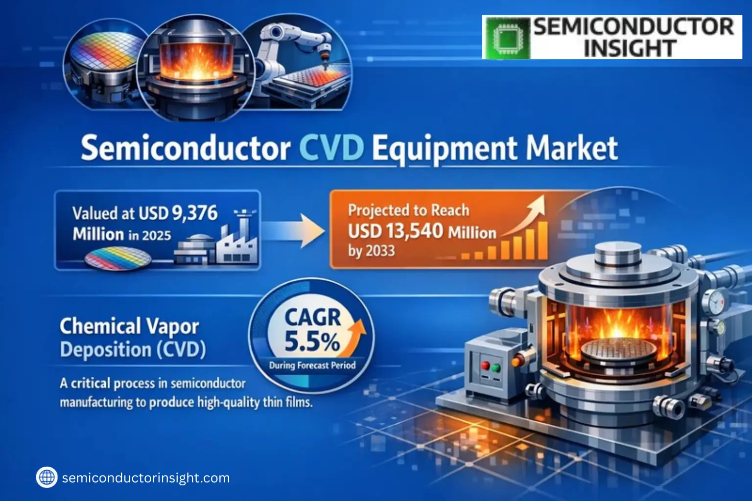
Global Semiconductor CVD Equipment Market was valued at USD 9,376 million in 2025 and is projected to reach USD 13,540 million by 2033, exhibiting a CAGR of 5.5% during the forecast period.
Chemical vapor deposition (CVD) is a critical process used in semiconductor manufacturing to produce high-quality thin films. The technique involves exposing substrates to volatile precursors that react or decompose on the surface, forming solid deposits while volatile byproducts are removed. CVD enables precise material deposition in various forms monocrystalline, polycrystalline, amorphous, and epitaxial essential for advanced semiconductor fabrication.
The market growth is driven by increasing demand for miniaturized electronic components and the expansion of foundry capacities worldwide. Key players like Applied Materials, Lam Research, and Tokyo Electron dominate the sector with a combined 73% market share. Geographically, China leads adoption with 28% market share due to aggressive semiconductor capacity expansions. Plasma-enhanced CVD (PECVD) remains the dominant technology segment at 51% share owing to its versatility in depositing dielectric films at lower temperatures.
MARKET DRIVERS
Growing Demand for Advanced Semiconductor Devices
Semiconductor CVD Equipment Market is experiencing steady growth due to increasing demand for high-performance chips in AI, 5G, and IoT applications. Leading semiconductor manufacturers are investing heavily in CVD technology to enhance production efficiency and yield rates. The market is projected to grow at a CAGR of 6.8% through 2030, driven by innovations in miniaturization and material science.
Technological Advancements in CVD Processes
Advanced deposition techniques such as atomic layer deposition (ALD) and plasma-enhanced CVD are gaining traction, enabling thinner, more uniform coatings. These innovations reduce material waste and improve device performance, further fueling adoption in the Semiconductor CVD Equipment Market.
Government initiatives supporting domestic semiconductor manufacturing are creating additional demand for CVD equipment worldwide.
MARKET CHALLENGES
High Capital and Operational Costs
Semiconductor CVD Equipment Market faces significant barriers due to the multi-million dollar investments required for advanced systems. Maintenance costs and the need for specialized operators further increase total cost of ownership, particularly for small and medium-sized manufacturers.
Other Challenges
Yield Management Complexities
Achieving consistent deposition quality across large-scale production remains technically challenging, with defect rates impacting overall product yields in the Semiconductor CVD Equipment Market.
MARKET RESTRAINTS
Supply Chain Disruptions and Component Shortages
Geopolitical tensions have created bottlenecks in the global Semiconductor CVD Equipment Market, with lead times for critical components extending beyond 12 months in some cases. This has delayed expansion plans for several major foundries and IDMs.
MARKET OPPORTUNITIES
Emerging Applications in Power Electronics
Semiconductor CVD Equipment Market is poised for growth in power device manufacturing, particularly for electric vehicles and renewable energy systems. CVD systems capable of processing wide-bandgap semiconductors like silicon carbide and gallium nitride present significant revenue opportunities.
Semiconductor CVD Equipment Market Trends
Steady Growth in Semiconductor CVD Equipment Demand
Global Semiconductor CVD Equipment Market continues its upward trajectory, valued at USD 9,376 million in 2025. Projections indicate robust expansion to USD 13,540 million by 2033, growing at a CAGR of 5.5%. This demand is primarily driven by increasing semiconductor fabrication across IDM companies and wafer foundries, supported by technological advancements in deposition processes.
Other Trends
PECVD Dominates Equipment Segments
Plasma-enhanced chemical vapor deposition (PECVD) maintains market leadership with 51% share, favored for its versatility in depositing dielectric films. The technique’s compatibility with temperature-sensitive substrates and superior throughput continues to drive adoption across semiconductor manufacturing facilities worldwide.
Regional Market Concentration
Asia-Pacific remains the dominant force in Semiconductor CVD Equipment consumption, with China alone accounting for 28% of global demand. The concentration of leading foundries and IDMs in South Korea and Taiwan further consolidates regional market position, while North America and Europe maintain steady growth through specialty applications.
Industry Consolidation Continues
The market remains concentrated with Applied Materials, Lam Research, and Tokyo Electron collectively holding 73% market share. Recent capacity expansions by these leaders reflect long-term confidence in semiconductor fabrication growth, particularly for advanced nodes below 10nm.
Emerging Process Technologies
Manufacturers are increasingly adopting Atomic Layer Deposition (ALD)-enhanced CVD systems to achieve superior film uniformity at sub-5nm nodes. This technological evolution addresses the industry’s needs for conformal coatings in 3D NAND and advanced logic devices, creating new opportunities for equipment innovation.
COMPETITIVE LANDSCAPE
Key Industry Players
Oligopolistic Market Dominated by Top 3 Players Controlling 73% Share
Semiconductor CVD Equipment Market exhibits a highly consolidated structure, with Applied Materials, Lam Research, and Tokyo Electron collectively commanding 73% of global market share. Applied Materials leads through its diversified PECVD and epitaxial systems, particularly dominating the 300mm wafer processing segment. Lam Research has strengthened its position through strategic acquisitions and advancements in atomic layer deposition (ALD)-enhanced CVD technologies. Tokyo Electron maintains strong foothold in Asian markets with specialized solutions for advanced node manufacturing.
Emerging players are gaining traction through niche segment focus: ASM International leads in single wafer ALD systems for EUV lithography applications, while Kokusai Electric specializes in batch processing CVD systems for memory manufacturers. Chinese manufacturers like Naura and Piotech are rapidly expanding capabilities to serve domestic semiconductor fabs, supported by government initiatives in semiconductor self-sufficiency. Veeco and CVD Equipment focus on specialized applications in compound semiconductors and advanced packaging.
List of Key Semiconductor CVD Equipment Companies Profiled
- Applied Materials
- Lam Research
- Tokyo Electron
- ASM International
- Kokusai Electric
- Wonik IPS
- Eugene Technology
- Jusung Engineering
- TES
- SPTS Technologies (KLA)
- Veeco
- CVD Equipment
- Piotech
- Naura
Segment Analysis:
| Segment Category | Sub-Segments | Key Insights |
| By Type |
|
PECVD dominates the semiconductor CVD equipment market due to:
|
| By Application |
|
IDM Companies represent the most significant application area because:
|
| By End User |
|
Memory Chip Producers are key adopters due to:
|
| By Material Type |
|
Silicon-based Materials maintain leadership position because:
|
| By Technology Node |
|
10nm and Below segment shows strongest demand growth due to:
|
Regional Analysis: Semiconductor CVD Equipment Market
Asia-Pacific leads in transitioning to sub-7nm nodes, requiring advanced CVD equipment for precise deposition. Foundries invest heavily in atomic layer deposition (ALD) systems to enable next-generation chips.
Regional governments provide tax incentives and subsidies for CVD equipment purchases. Strategic partnerships between public institutions and semiconductor firms accelerate technology development.
Concentrated semiconductor clusters in Hsinchu (Taiwan) and Suzhou (China) create demand synergies for CVD equipment. Proximity to component suppliers reduces lead times for maintenance and upgrades.
Strong technical education systems produce skilled engineers for CVD equipment operation. Universities collaborate with semiconductor firms on specialized deposition process research.
North America
North America maintains technological leadership in semiconductor CVD equipment innovation, housing major equipment manufacturers like Applied Materials and Lam Research. The region benefits from extensive R&D investments in next-generation deposition technologies and strategic collaborations between equipment suppliers and semiconductor fabs. While manufacturing has declined, the US CHIPS Act is driving renewed domestic production capacity. Silicon Valley remains the global hub for CVD equipment design and process development, supported by access to venture capital and cutting-edge research institutions.
Europe
Europe specializes in niche CVD equipment for power semiconductors and MEMS applications, with strong capabilities in deposition technologies for automotive and industrial chips. The EU Chips Act aims to strengthen regional semiconductor self-sufficiency, potentially boosting CVD equipment demand. Leading research institutes like IMEC in Belgium contribute to advanced deposition process development. Germany’s strong industrial base supports demand for specialized CVD systems tailored for automotive and industrial applications.
Middle East & Africa
The region shows nascent growth in semiconductor CVD equipment adoption, primarily serving local packaging and testing facilities. Government initiatives in the Gulf Cooperation Council countries aim to develop semiconductor manufacturing capabilities. Limited local fabrication capacity currently constrains equipment demand, but strategic investments in technology transfer could create new opportunities. Partnerships with Asian and European firms are establishing a foundation for future CVD equipment market growth.
South America
South America represents an emerging market for semiconductor CVD equipment, with Brazil leading in regional semiconductor manufacturing. Market growth faces challenges from limited infrastructure and investment, though some countries are developing specialized fabrication capabilities. Local demand primarily stems from consumer electronics assembly and automotive component manufacturing. The region shows potential for gradual CVD equipment adoption as regional free trade agreements facilitate technology transfer.
Report Scope
This market research report provides a comprehensive analysis of the Semiconductor CVD Equipment Market, covering the forecast period 2025–2033. It offers detailed insights into market dynamics, technological advancements, competitive landscape, and key trends shaping the industry.
Key focus areas of the report include:
- Market Overview: The report begins with an overview outlining its current market scenario, key growth indicators, and industry transformation drivers. It discusses macroeconomic factors, demand–supply balance, regulatory landscape, and the strategic role of semiconductor manufacturing equipment in powering advancements across industries such as consumer electronics, automotive, industrial automation, and telecommunications.
- Market Size & Forecast: Historical data and future projections for revenue, unit shipments, and market value across major regions and segments.
- Segmentation Analysis: Detailed breakdown by product type, technology, application, and end-user industry to identify high-growth segments and investment opportunities.
- Regional Insights: Insights into market performance across North America, Europe, Asia-Pacific, Latin America, and the Middle East & Africa, including country-level analysis where relevant.
- Competitive Landscape: Profiles of leading market participants, including their product offerings, R&D focus, manufacturing capacity, pricing strategies, and recent developments such as mergers, acquisitions, and partnerships.
- Technology Trends & Innovation: Assessment of emerging technologies, semiconductor design trends, fabrication techniques, and evolving industry standards.
- Market Drivers & Restraints: Evaluation of factors driving market growth along with challenges, supply chain constraints, regulatory issues, and market-entry barriers.
- Stakeholder Insights: Insights for equipment manufacturers, foundries, IDM companies, investors, and policymakers regarding the evolving ecosystem and strategic opportunities.
Primary and secondary research methods are employed, including interviews with industry experts, data from verified sources, and real-time market intelligence to ensure the accuracy and reliability of the insights presented.
FREQUENTLY ASKED QUESTIONS:
What is the current market size of Semiconductor CVD Equipment Market?
-> Semiconductor CVD Equipment Market was valued at USD 9,376 million in 2025 and is projected to reach USD 13,540 million by 2033, exhibiting a CAGR of 5.5% during the forecast period.
Which key companies operate in Semiconductor CVD Equipment Market?
-> Key players include Applied Materials, Lam Research, Tokyo Electron, ASM International, Kokusai Electric, Wonik IPS, Eugene Technology, Jusung Engineering, TES, SPTS Technologies (KLA), Veeco, CVD Equipment, Piotech, and Naura. The top three players hold about 73% market share.
What are the key growth drivers?
-> Key growth drivers include rising semiconductor demand, advancements in microfabrication technologies, expansion of wafer foundries, and increasing adoption of advanced materials like high-k dielectrics and graphene.
Which region dominates the market?
-> China is the largest market accounting for 28% share, followed by South Korea and Taiwan. Asia-Pacific dominates the global Semiconductor CVD Equipment Market.
What are the emerging trends?
-> Emerging trends include development of advanced CVD techniques, integration of AI in semiconductor manufacturing, and increasing demand for PECVD equipment (51% market share).

Get Sample Report PDF for Exclusive Insights
Report Sample Includes
- Table of Contents
- List of Tables & Figures
- Charts, Research Methodology, and more...


