
Sapphire Polish Wafer Market Insights
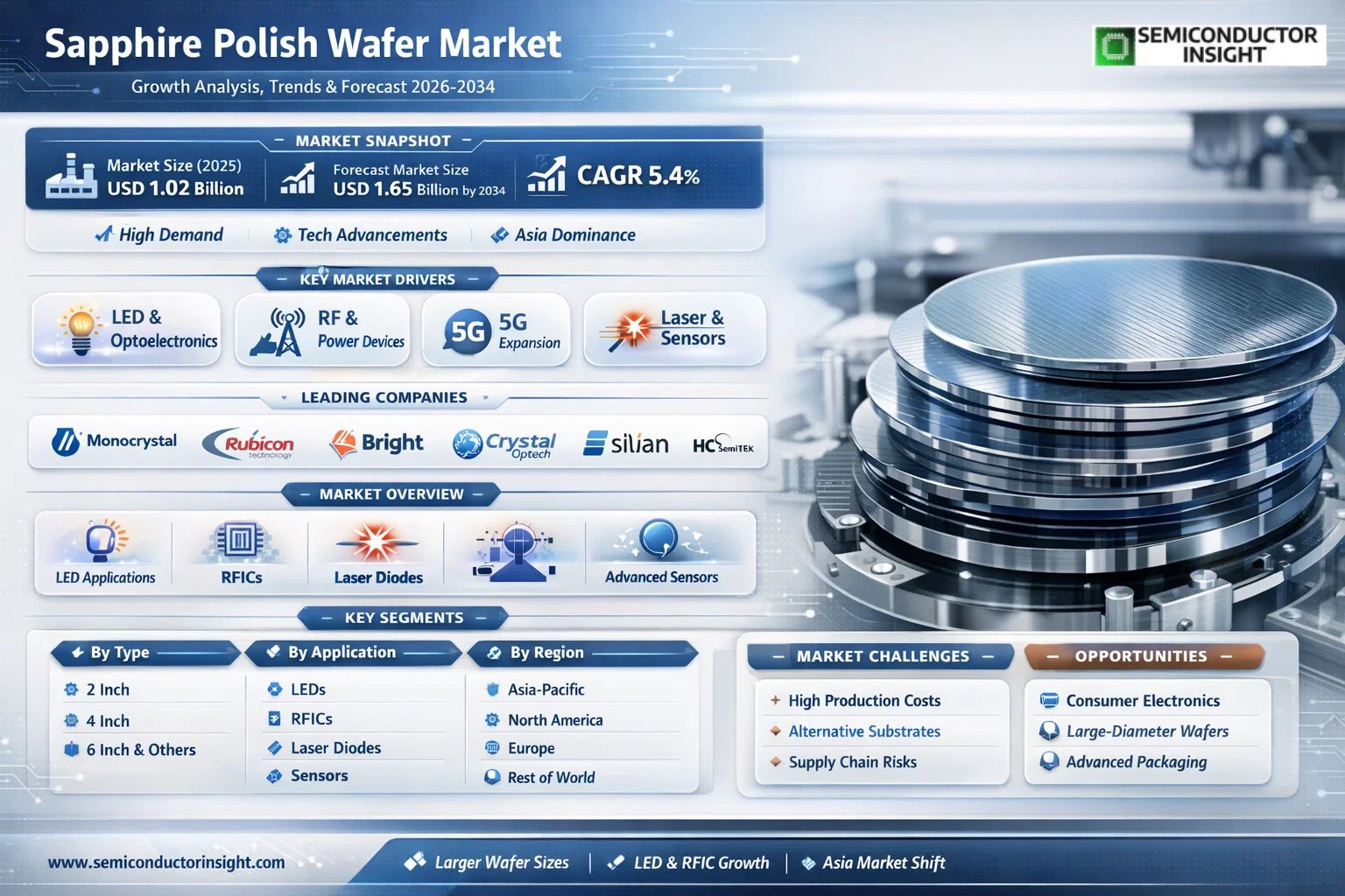
Global sapphire polish wafer market size was valued at USD 1.02 billion in 2025. The market is projected to grow from USD 1.08 billion in 2026 to USD 1.65 billion by 2034, exhibiting a CAGR of 5.4% during the forecast period.
Sapphire polish wafers are high-purity, single-crystal aluminum oxide (Al₂O₃) substrates that have undergone precision polishing to achieve an atomically smooth, defect-free surface. These wafers are crucial substrates for epitaxial growth in semiconductor and optoelectronic manufacturing because sapphire offers excellent thermal stability, high hardness, and good electrical insulation. Key applications include serving as the foundational material for manufacturing Light Emitting Diodes (LEDs), particularly blue and white LEDs, as well as for Radio Frequency Integrated Circuits (RFICs), laser diodes, and specialized sensors.
The market’s growth is primarily driven by the sustained demand in the LED industry, which consumes a significant volume of sapphire wafers, especially in the 4-inch and 6-inch diameters for high-brightness applications. Furthermore, the expansion of 5G infrastructure and wireless communication is boosting demand for RFICs that utilize sapphire substrates due to their low signal loss properties. However, the market faces challenges from cyclical downturns in the broader semiconductor sector and competitive pressure from alternative substrates like silicon carbide (SiC) and gallium nitride (GaN) on silicon for certain applications. Recent industry developments include capacity expansions by key players in Asia to meet growing demand; for instance, several Chinese manufacturers have increased their production of large-diameter polished wafers to improve economies of scale. Leading companies operating in this competitive landscape include Monocrystal, Rubicon Technology Inc., Crystal Optech, and San’an Optoelectronics.
MARKET DRIVERS
Strong Demand from LED & Optoelectronics
The core growth driver for the Sapphire Polish Wafer Market remains its critical role as a substrate for Gallium Nitride (GaN) epitaxy in LED manufacturing. Global transition to energy-efficient lighting and the proliferation of micro-LEDs and mini-LEDs for advanced displays necessitate wafers with exceptional surface quality. A polished sapphire wafer provides the atomically smooth, defect-free surface required for high-yield, high-performance epi-layer growth, directly linking market expansion to the optoelectronics industry’s innovation cycle.
Adoption in Radio Frequency and Power Devices
Beyond lighting, sapphire’s excellent electrical insulation and thermal stability are driving its evaluation and adoption for Radio Frequency (RF) applications and power electronics. As a substrate for high-electron-mobility transistors (HEMTs), a polished sapphire wafer can support devices operating at higher frequencies and power densities. This expansion into new semiconductor segments diversifies demand and reduces reliance on a single end-market.
➤ A key enabler for this demand is the continuous improvement in Chemical Mechanical Polishing (CMP) processes, which achieve surface roughness below 0.2 nm, meeting the stringent requirements of next-generation semiconductor fabrication.
The push for device miniaturization and higher performance specifications across the semiconductor industry mandates substrates of unparalleled quality. This creates a fundamental, technology-driven demand for advanced polishing services and finished wafers within the Sapphire Polish Wafer Market.
MARKET CHALLENGES
High Production Cost and Process Complexity
A primary challenge in the Sapphire Polish Wafer Market is the significant cost structure. The processes of growing high-purity sapphire crystals via methods like Kyropoulos or Heat Exchanger Method (HEM), followed by precise slicing, grinding, and multi-stage polishing, are capital and energy-intensive. The stringent defect and flatness tolerances required by leading-edge applications result in lower yield rates, further exacerbating cost pressures and creating a barrier for price-sensitive market segments.
Other Challenges
Competition from Alternative Substrates
The market faces continuous competitive pressure from materials like silicon carbide (SiC) and silicon (Si), particularly in power semiconductor and certain RF applications. While sapphire offers distinct advantages in LED and specific optoelectronic uses, competing substrates are achieving cost reductions and performance improvements that challenge sapphire’s value proposition in new application areas.
Supply Chain and Geopolitical Sensitivities
The concentration of advanced polishing expertise and crystal growth capacity in specific geographic regions creates supply chain vulnerabilities. Trade policies, export controls, and raw material availability can introduce volatility and uncertainty for global consumers of polished sapphire wafers, complicating long-term planning and procurement strategies for device manufacturers.
MARKET RESTRAINTS
Economic Cyclicality of End-User Industries
The Sapphire Polish Wafer Market is intrinsically linked to the investment and production cycles of its primary consumers, namely the LED, consumer electronics, and automotive sectors. Capital expenditure downturns or demand softening in these industries lead directly to reduced orders for substrates, creating pronounced cyclicality. This dependence restrains steady, predictable growth for wafer manufacturers and polishers, necessitating robust financial planning to weather industry downturns.
Technical Limitations for Ultra-High Power Applications
While excellent for many applications, sapphire’s lower thermal conductivity compared to substrates like silicon carbide acts as a technical restraint for ultra-high-power and high-temperature semiconductor devices. This intrinsic material property limits its penetration into the most demanding segments of the power electronics market, capping its addressable market share where thermal management is the paramount design constraint.
MARKET OPPORTUNITIES
Emergence of Novel Consumer and Defense Applications
The unique properties of polished sapphire, including its exceptional hardness and optical clarity, are unlocking opportunities beyond traditional semiconductors. Its use in cover glass for premium consumer electronics, wearable sensors, and as optical windows in defense and aerospace systems represents a high-value growth avenue. These applications often command higher margins and are less sensitive to the cost pressures prevalent in the high-volume LED sector.
Innovation in Large-Diameter Wafer Polishing
A significant opportunity lies in the scaling of wafer diameters. Transitioning from mainstream 4-inch and 6-inch wafers to larger 8-inch formats offers substantial efficiency gains for device manufacturers by increasing die-per-wafer count. Companies that master the polishing and finishing of larger-diameter sapphire wafers with high uniformity will secure a competitive advantage and cater to the semiconductor industry’s relentless drive for manufacturing economies of scale.
Advanced Packaging and Heterogenous Integration
The trend toward advanced packaging and heterogenous integration presents a promising frontier. Sapphire can be utilized as a carrier wafer or interposer due to its high rigidity and thermal stability during complex packaging processes like fan-out wafer-level packaging (FO-WLP). This application leverages the polished sapphire wafer’s physical properties in a novel context, opening a parallel market segment alongside its traditional substrate role.
Analysing the Sapphire Polish Wafer Market: Key Industry Trends
Demand for Larger Wafer Sizes Driving Technological Evolution
The predominant trend in the Sapphire Polish Wafer Market is the clear shift towards larger diameter substrates. While 2-inch and 4-inch wafers remain in production for niche applications, there is significant industry emphasis on scaling up to 6-inch and larger formats. This transition is driven by the relentless pursuit of manufacturing efficiency in end-use industries, particularly for Light Emitting Diode (LED) production. Larger Sapphire Polish Wafers provide greater surface area, allowing for more chips to be produced per wafer, which directly reduces the overall cost per device. This trend necessitates continuous advancements in crystal growth and polishing technologies to maintain the exceptional surface flatness and minimal subsurface damage required for high-performance semiconductor and optoelectronic devices.
Other Trends
Consolidation of Application Segments
Application landscape for the Sapphire Polish Wafer Market is consolidating around high-growth sectors, with Light Emitting Diodes (LEDs) continuing to dominate demand. This is closely followed by expanding use in specialized Radio Frequency Integrated Circuits (RFICs) and Laser Diodes, where the material’s superior thermal and electrical insulation properties are critical. The ‘Others’ segment, while smaller, is seeing innovative applications in areas like advanced sensors and power electronics, indicating potential future growth avenues beyond the current primary uses.
Geographical Production and Demand Realignment
A significant market trend is the ongoing realignment between production hubs and demand centers. The Asia-Pacific region, particularly China, Japan, and South Korea, represents both a major manufacturing base for Sapphire Polish Wafers and the largest consumption market, driven by their massive electronics and LED industries. However, recent regional demand fluctuations, as observed in broader semiconductor sales data, highlight the market’s sensitivity to global economic conditions. This is prompting companies to diversify supply chains and explore growth in other regions like the Americas and Europe, where demand for specialized components in automotive and industrial applications is creating new opportunities for Sapphire Polish Wafer suppliers.
COMPETITIVE LANDSCAPE
Key Industry Players
A Specialized and Capital-Intensive Market
Global sapphire polish wafer market is highly consolidated, with a few specialized manufacturers holding significant market share due to the intense capital requirements and technological expertise needed for high-volume, high-crystallographic-quality production. Industry leader Monocrystal is a dominant force, renowned for its vertically integrated production from crystal growth to polished wafers and its strong position supplying the LED and optoelectronics sectors. Similarly, Rubicon Technology and HC SemiTek Corporation are pivotal players with substantial global production capacities. The competitive structure is defined by continuous R&D investments to produce larger diameter wafers (such as 6-inch and above) with superior surface quality and TTV (Total Thickness Variation) to meet the stringent demands of applications like RFICs and laser diodes.
Beyond these top-tier players, several significant regional competitors have carved out strong niches. In China, companies like San’an Optoelectronics and Silian hold considerable domestic market share, supported by the region’s expansive LED manufacturing ecosystem. Meanwhile, firms such as Bright (Shengda Group) and Crystal Optech compete effectively in specific wafer diameters and polishing grades. Other key participants, including Sinopatt, TDG, and Unionlight Technology, focus on specialized polishing services and tailored wafer solutions for emerging applications, creating a multi-layered competitive environment where technology, cost, and regional supply chains are critical differentiators.
List of Key Sapphire Polish Wafer Companies Profiled
- Monocrystal
- Rubicon Technology, Inc.
- Bright (Shengda Group)
- Crystal Optech
- Silian
- Sinopatt
- TDG Holding Co., Ltd.
- HC SemiTek Corporation
- San’an Optoelectronics Co., Ltd.
- Unionlight Technology
- Guizhou Haotian Optoelectronics Technology Co., Ltd.
- KYOCERA Corporation
- Precision Micro-Optics Inc.
- Rayotek Scientific Inc.
- Crystalwise Technology Inc.
Segment Analysis:
| Segment Category | Sub-Segments | Key Insights |
| By Type |
|
6 Inch wafers represent the leading segment, driven by the critical need for larger substrate areas to enhance manufacturing efficiency and yield for high-volume electronics. This dimension offers a superior balance between production throughput and material utilization, making it highly desirable for advanced semiconductor fabrication. The growth is further propelled by investments in next-generation LED and power device production lines that require the superior thermal and electrical insulation properties of sapphire on a larger scale. |
| By Application |
|
Light Emitting Diode (LED) remains the dominant application segment, as sapphire’s structural properties provide an ideal lattice-matched substrate for high-brightness and energy-efficient GaN-based LED epitaxy. The relentless global push for energy conservation and the expansion of smart lighting, automotive lighting, and display backlighting continuously fuel demand. Furthermore, technological advancements in micro-LED and mini-LED displays for consumer electronics are opening new, high-value avenues for ultra-polished sapphire wafers, securing this segment’s leadership. |
| By End User |
|
LED Manufacturers constitute the primary and most influential end-user segment, directly driving volume consumption and technical specifications for polish wafers. This dominance is linked to mass production needs for general illumination and consumer electronics. These manufacturers exert significant influence on supply chain dynamics, polish quality standards, and pricing, fostering deep, strategic partnerships with key wafer suppliers to ensure a consistent flow of high-quality substrates essential for maintaining their competitive edge in a fast-evolving market. |
| By Polish Grade |
|
Prime/High-Epitaxial Grade is the leading segment, characterized by its exceptionally low surface roughness and minimal defect density, which are non-negotiable for high-performance semiconductor device fabrication. The demand for this premium grade is intensifying as device architectures become more complex and sensitive to substrate imperfections, particularly for RFICs and advanced laser diodes. This trend reflects the industry’s shift towards higher quality and reliability over pure cost considerations, with manufacturers willing to invest in superior substrates to maximize end-device yield and performance. |
| By Supply Chain Role |
|
Integrated Manufacturers, who control the process from crystal growth to final polished wafer, hold a commanding position. This vertical integration provides critical advantages in quality control, production schedule consistency, and proprietary technology development, creating high barriers to entry for smaller players. Their dominance allows for tighter specification management and rapid response to application-specific customer requirements, making them pivotal in driving industry standards and innovation in polishing techniques to meet the evolving demands of the optoelectronics and semiconductor sectors. |
Regional Analysis: Asia-Pacific
Asia-Pacific: The Dominant Powerhouse
This sub-region represents the technological apex for the Sapphire Polish Wafer Market, driven by world-leading semiconductor foundries and display manufacturers. The demand is characterized by an unrelenting need for ultra-smooth, defect-free wafers for applications in micro-LEDs and RF devices. Local polishing technology providers work in close partnership with major fabs, creating a feedback loop that accelerates process improvements and sets global quality benchmarks for surface finish and flatness.
China’s market is defined by immense scale and a strategic drive to control the entire materials supply chain. The domestic Sapphire Polish Wafer Market is fueled by a vast LED packaging industry and growing investments in GaN-on-sapphire for power electronics. Government initiatives supporting domestic semiconductor equipment and materials suppliers are fostering local capacity, impacting regional supply dynamics and competitive pricing for polishing services and consumables.
Japan maintains a strong position through its leadership in precision machining and polishing equipment, which is critical to the Sapphire Polish Wafer Market ecosystem. Japanese firms excel in supplying the advanced slurries, polishing pads, and metrology tools required for high-end wafer finishing. This expertise supports demanding applications in laser optics and sensors, making Japan an indispensable hub for high-value, specialized segments of Global polishing market.
Southeast Asia is emerging as an important growth frontier, attracting investments in semiconductor assembly and packaging. While not yet a major center for primary wafer polishing, this sub-region’s expansion in back-end manufacturing is increasing the demand for polished wafers for final device integration. It serves as a complementary production base that supports the broader Asia-Pacific Sapphire Polish Wafer Market supply chain.
North America
The North American Sapphire Polish Wafer Market is characterized by high-value, innovation-driven demand, particularly from the defense, aerospace, and optoelectronics sectors. The region hosts leading companies involved in RF filter production for 5G infrastructure and advanced research in photonic integrated circuits, which require wafers with exceptional surface quality. While manufacturing volume is less than Asia-Pacific, the focus on cutting-edge applications in power electronics and specialized sensors creates a premium market segment. Collaborative environments between national labs, universities, and private firms drive advancements in wafer polishing techniques for next-generation semiconductor devices.
Europe
Europe maintains a significant presence in the Sapphire Polish Wafer Market through its strong automotive industrial base and leadership in research institutions. The demand is closely tied to the automotive sector’s shift towards electric vehicles and advanced driver-assistance systems (ADAS), which utilize sapphire-based sensors and LED lighting. Key markets like Germany and France have a concentration of firms specializing in high-precision optics and laser systems, fostering demand for meticulously polished wafers. European Union funding for compound semiconductor initiatives further supports regional market development for specialized sapphire applications.
South America
The South American market for Sapphire Polish Wafers is currently niche and developing, with primary demand linked to research activities and limited industrial applications in telecommunications infrastructure. Brazil represents the most active country, with some demand emerging from academic and governmental research institutes focusing on materials science. The market growth is constrained by the lack of a large-scale local semiconductor fabrication ecosystem. However, regional investments in upgrading telecom networks could gradually stimulate demand for polished wafers used in optical components over the long term.
Middle East & Africa
The Middle East & Africa region holds a minor share in Global Sapphire Polish Wafer Market, with activity largely concentrated in a few technological enclaves. The Gulf Cooperation Council (GCC) nations are making strategic investments in technology diversification, which could lead to future demand for advanced materials like polished sapphire wafers for specialized electronics and sensing projects. South Africa has some research capabilities in mining-related sensor technology. Overall, market dynamics are defined by nascent demand, with growth dependent on long-term technology transfer and infrastructure development initiatives.
Report Scope
This market research report provides a comprehensive analysis of the Sapphire Polish Wafer Market , covering the forecast period 2026–2034. It offers detailed insights into market dynamics, technological advancements, competitive landscape, and key trends shaping the industry.
Key focus areas of the report include:
- Market Overview: The report begins with an overview outlining the current market scenario, key growth indicators, and industry transformation drivers. It discusses macroeconomic factors, demand–supply balance, regulatory landscape, and the strategic role of semiconductors in powering advancements across industries such as automotive, telecommunications, consumer electronics, and industrial automation.
- Market Size & Forecast: Historical data and future projections for revenue, unit shipments, and market value across major regions and segments.
- Segmentation Analysis: Detailed breakdown by product type, technology, application, and end-user industry to identify high-growth segments and investment opportunities.
- Regional Insights: Insights into market performance across North America, Europe, Asia-Pacific, Latin America, and the Middle East & Africa, including country-level analysis where relevant.
- Competitive Landscape: Profiles of leading market participants, including their product offerings, R&D focus, manufacturing capacity, pricing strategies, and recent developments such as mergers, acquisitions, and partnerships.
- Technology Trends & Innovation: Assessment of emerging technologies, integration of AI/IoT, semiconductor design trends, fabrication techniques, and evolving industry standards.
- Market Drivers & Restraints: Evaluation of factors driving market growth along with challenges, supply chain constraints, regulatory issues, and market-entry barriers.
- Stakeholder Insights: Insights for component suppliers, OEMs, system integrators, investors, and policymakers regarding the evolving ecosystem and strategic opportunities.
Primary and secondary research methods are employed, including interviews with industry experts, data from verified sources, and real-time market intelligence to ensure the accuracy and reliability of the insights presented.
FREQUENTLY ASKED QUESTIONS:
What is the current market size of Sapphire Polish Wafer Market?
-> Global Sapphire Polish Wafer market was valued at USD million in 2025 and is projected to reach USD million by 2034, at a CAGR of % during the forecast period.
Which key companies operate in Sapphire Polish Wafer Market?
-> Key players include Monocrystal, Rubicon Technology, Bright, Crystal Optech, Silian, Sinopatt, TDG, HC SemiTek Corporation, San’an Optoelectronics, and Unionlight Technology, among others.
What are the key growth drivers?
-> Key growth drivers include advancements in semiconductor applications such as LEDs, RFICs, and laser diodes, alongside ongoing global infrastructure investments in telecommunications and consumer electronics.
Which region dominates the market?
-> Asia-Pacific is the largest region for semiconductor sales, though the broader Asia-Pacific region experienced a sales decline of 2.0% year-on-year in 2022, while other regions like the Americas and Europe showed double-digit growth.
What are the emerging trends?
-> Emerging trends include increasing demand from the LED sector, the application in RFICs and laser diodes, and technological advancements in wafer fabrication and polishing techniques.

Get Sample Report PDF for Exclusive Insights
Report Sample Includes
- Table of Contents
- List of Tables & Figures
- Charts, Research Methodology, and more...
 Download Sample Report PDF



