MARKET INSIGHTS
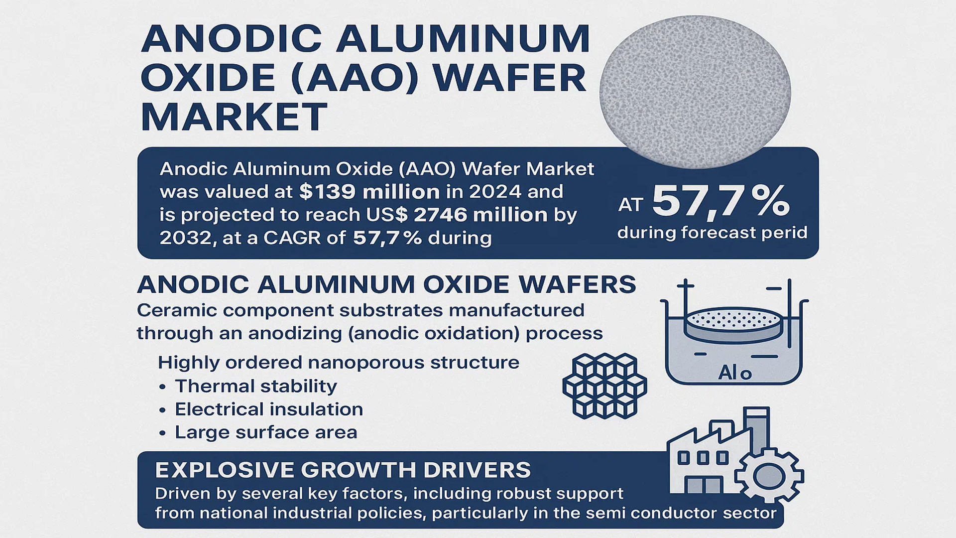
The global Anodic Aluminum Oxide (AAO) Wafer Market was valued at 139 million in 2024 and is projected to reach US$ 2746 million by 2032, at a CAGR of 57.7% during the forecast period.
Anodic Aluminum Oxide (AAO) wafers are ceramic component substrates manufactured through an anodizing (anodic oxidation) process. This technology involves growing an oxide film on the surface of aluminum by applying an electric charge after immersing it in an electrolyte solution. These wafers are critical substrates in advanced semiconductor manufacturing and nanotechnology applications due to their highly ordered nanoporous structure, which provides excellent thermal stability, electrical insulation, and a large surface area.
The market is experiencing explosive growth driven by several key factors, including robust support from national industrial policies, particularly in the semiconductor sector. For instance, China’s substantial investments in semiconductor self-sufficiency are creating significant downstream demand. Furthermore, continuous technological innovation from manufacturers striving to remain competitive is accelerating product development. The rapid expansion of transformative technologies such as 5G, artificial intelligence (AI), and the Internet of Things (IoT) is also fueling demand for advanced semiconductors, which in turn increases the need for high-performance AAO wafers. North America currently dominates production, holding over 51% of the market share, while the 4-inch wafer size is the largest product segment, accounting for more than 34% of sales. The primary application is in packaging & foundry, which constitutes over 77% of the market. Key players such as InRedox and Point Engineering are central to the market’s expansion, driving innovation and capacity to meet this surging global demand.
MARKET DYNAMICS
MARKET DRIVERS
Robust Semiconductor Industry Expansion to Propel AAO Wafer Demand
The global semiconductor industry is experiencing unprecedented growth, with revenues exceeding $600 billion annually, driving substantial demand for advanced materials like Anodic Aluminum Oxide wafers. These specialized substrates have become critical components in semiconductor manufacturing processes, particularly in packaging and foundry applications where they account for over 77% of total AAO wafer usage. The ongoing miniaturization of electronic components and increasing complexity of integrated circuits require superior thermal management and electrical insulation properties that AAO wafers provide exceptionally well. This technological necessity, combined with the semiconductor industry’s compound annual growth rate of approximately 8-10%, creates a powerful upward trajectory for AAO wafer adoption across global manufacturing facilities.
Government Initiatives and Strategic Investments in Semiconductor Infrastructure
National policies worldwide are accelerating semiconductor independence and technological sovereignty, creating favorable conditions for AAO wafer market expansion. Several countries have launched comprehensive semiconductor development programs with committed investments totaling over $200 billion globally. These initiatives specifically target advanced materials development, including substrate technologies that enhance semiconductor performance and reliability. The substantial financial backing from public and private sectors enables research institutions and manufacturing facilities to accelerate AAO wafer technology adoption and scale production capabilities to meet growing industry demands.
Emerging Technologies and Next-Generation Applications Driving Innovation
The rapid advancement of 5G networks, artificial intelligence systems, and Internet of Things applications is creating new semiconductor requirements that directly benefit AAO wafer manufacturers. These technologies demand higher processing speeds, increased power efficiency, and enhanced thermal management – all areas where AAO wafers demonstrate significant advantages over traditional substrates. The global AI chip market alone is projected to grow at approximately 35% CAGR, requiring specialized semiconductor components that utilize advanced materials like anodic aluminum oxide. This technological convergence is pushing manufacturers to develop increasingly sophisticated AAO wafers that can meet the rigorous performance standards of next-generation electronic devices and systems.
MARKET CHALLENGES
High Production Costs and Complex Manufacturing Processes
The AAO wafer market faces significant challenges related to production economics and technical complexity. Manufacturing these specialized substrates requires precise control of anodization parameters, ultra-pure aluminum sources, and sophisticated quality control systems that contribute to substantially higher production costs compared to conventional semiconductor substrates. The specialized equipment needed for consistent AAO wafer production represents a capital investment of $15-20 million per production line, creating substantial barriers to entry for new market participants. Additionally, maintaining consistent pore structure and thickness across wafer surfaces demands exceptionally tight process controls that can challenge even established manufacturers.
Other Challenges
Technical Performance Limitations
While AAO wafers offer excellent thermal and electrical properties, they face challenges in mechanical strength and handling characteristics compared to silicon-based substrates. The ceramic nature of anodic aluminum oxide makes wafers more susceptible to cracking during processing and packaging operations, potentially affecting yield rates in high-volume manufacturing environments. These technical limitations require additional handling precautions and specialized equipment, adding to overall production costs and complexity.
Supply Chain Vulnerabilities
The AAO wafer manufacturing process depends on consistent supplies of high-purity aluminum and specialized chemical reagents, creating potential vulnerabilities in the supply chain. Price fluctuations in raw materials, coupled with geopolitical factors affecting metal markets, can significantly impact production costs and planning. Recent disruptions in global supply chains have highlighted these vulnerabilities, with some manufacturers experiencing cost increases of 20-30% for critical input materials.
MARKET RESTRAINTS
Technical Standardization and Quality Consistency Issues
The absence of universally accepted technical standards for AAO wafers presents significant restraints on market growth. Different manufacturers employ varying anodization processes, electrolyte compositions, and quality control methodologies, resulting in products with differing performance characteristics. This lack of standardization complicates integration into semiconductor manufacturing processes where consistency and predictability are paramount. Semiconductor fabricators require extremely tight specifications with thickness variations limited to less than ±2% and pore density consistency within ±3% across entire wafer surfaces – specifications that challenge even the most advanced AAO production facilities.
Limited Production Capacity and Geographic Concentration
Current AAO wafer manufacturing remains heavily concentrated in specific geographic regions, with North America accounting for over 51% of global production capacity. This geographic concentration creates potential supply chain risks and limits market accessibility for semiconductor manufacturers in other regions. The specialized nature of AAO production means that establishing new manufacturing facilities requires significant technical expertise and capital investment, typically requiring 18-24 months from planning to full production capacity. This extended timeline creates challenges in rapidly responding to increased market demand, potentially constraining growth during periods of industry expansion.
Competition from Alternative Substrate Technologies
AAO wafers face increasing competition from emerging substrate technologies that offer alternative solutions for semiconductor applications. Advanced silicon-based substrates, composite materials, and novel ceramic compounds are being developed with improved performance characteristics and potentially lower production costs. These competing technologies are receiving substantial research funding, with annual investments exceeding $500 million globally for advanced substrate development. While AAO wafers currently maintain specific performance advantages, ongoing innovations in alternative materials could erode their market position unless manufacturers continue to advance AAO technology and reduce production costs.
MARKET OPPORTUNITIES
Expansion into New Application Areas Beyond Traditional Semiconductors
The unique properties of AAO wafers create significant opportunities beyond conventional semiconductor applications. Emerging fields including photonic devices, biomedical sensors, and energy storage systems are increasingly adopting AAO technology due to its excellent surface properties and tunable porosity. The global market for advanced sensors alone is projected to reach $350 billion by 2030, representing substantial potential for AAO wafer integration. These new application areas often have less stringent technical requirements than semiconductor manufacturing while offering higher profit margins, creating attractive diversification opportunities for established AAO producers.
Technological Advancements in Manufacturing Processes
Recent breakthroughs in anodization technology and process control systems are creating opportunities for significant quality improvements and cost reductions. Advanced electrochemical processes now enable more precise control of pore size distribution and thickness uniformity, potentially increasing production yields by 15-20% while reducing material waste. These technological advancements, combined with automation and Industry 4.0 implementation, are transforming AAO wafer manufacturing from a artisanal process to a highly controlled industrial operation. Manufacturers investing in these advanced production technologies can achieve substantial competitive advantages in both product quality and production economics.
Strategic Partnerships and Vertical Integration Opportunities
The growing importance of AAO wafers in advanced semiconductor manufacturing is driving increased interest from major technology companies seeking secure supply chains for critical components. This environment creates excellent opportunities for strategic partnerships, joint ventures, and potential acquisition activities. Semiconductor manufacturers are increasingly willing to establish long-term supply agreements and provide technical collaboration to ensure consistent access to high-quality AAO wafers. These partnerships often include shared development efforts and guaranteed purchase volumes, providing AAO producers with more predictable revenue streams and opportunities for technology co-development.
ANODIC ALUMINUM OXIDE (AAO) WAFER MARKET TRENDS
Technological Advancements in Semiconductor Fabrication to Emerge as a Key Trend
The semiconductor industry’s relentless pursuit of miniaturization and enhanced performance is fundamentally driving innovation in substrate materials, with Anodic Aluminum Oxide (AAO) wafers emerging as a critical enabler. These wafers are prized for their highly ordered, nanoporous structure, which is engineered through a precisely controlled electrochemical anodization process. This unique architecture is increasingly vital for creating advanced templates for nanowire growth, photonic crystals, and filtration membranes used in next-generation chip manufacturing. The market is witnessing a significant shift towards larger diameter wafers, with the 6-inch segment experiencing accelerated growth as it offers a more cost-effective surface area for high-volume production. Furthermore, process innovations are focusing on achieving unparalleled pore uniformity and aspect ratios, which are essential for the reproducibility required in commercial semiconductor fabrication. The ability to tailor pore diameters from 20 to 400 nanometers allows for incredible design flexibility, meeting the stringent specifications of emerging technologies like quantum computing components and ultra-high-density memory storage.
Other Trends
Expansion of 5G and IoT Infrastructure
The global rollout of 5G networks and the proliferation of Internet of Things (IoT) devices are creating an insatiable demand for high-performance semiconductors, which in turn fuels the need for advanced fabrication materials like AAO wafers. These wafers are integral in the production of radio frequency (RF) filters, power amplifiers, and sensors that form the backbone of 5G infrastructure and smart devices. The requirement for components that operate at higher frequencies with greater efficiency and lower power consumption directly benefits from the precise nanostructuring capabilities of AAO technology. This trend is further amplified by massive investments in smart city projects and industrial automation, which rely on a vast network of connected sensors and edge computing devices, all dependent on semiconductors fabricated using these advanced substrate materials.
Geopolitical and Policy-Driven Supply Chain Reshoring
Intensifying geopolitical tensions and a focus on supply chain security are prompting major economies to aggressively invest in domestic semiconductor production capabilities, a movement that significantly benefits the AAO wafer market. Initiatives like the CHIPS and Science Act in the United States, which allocates over $52 billion in funding for semiconductor research and manufacturing, are creating a fertile environment for advanced materials suppliers. Similarly, ambitious national strategies in China, South Korea, and across the European Union are prioritizing semiconductor sovereignty. This policy-driven push is not only increasing capital expenditure in new fabrication plants but also accelerating the adoption of sophisticated materials like AAO wafers to achieve technological independence and maintain a competitive edge. This trend is leading to increased collaboration between material science firms and integrated device manufacturers (IDMs) to develop bespoke AAO solutions that meet the specific requirements of cutting-edge nodes and packaging technologies, such as advanced fan-out wafer-level packaging (FOWLP) and 3D integration.
COMPETITIVE LANDSCAPE
Key Industry Players
Technological Innovation and Strategic Expansion Define Market Leadership
The global Anodic Aluminum Oxide (AAO) Wafer market exhibits a dynamic and evolving competitive structure, characterized by a blend of specialized technology providers and established materials science corporations. While the market is still developing, it demonstrates traits of consolidation around key technological innovators who hold critical patents and manufacturing expertise. InRedox LLC has emerged as a significant force, primarily due to its proprietary anodization processes and strong foothold in the North American market, which accounts for over 51% of global production. The company’s focus on high-precision, nanoporous AAO templates for semiconductor and research applications has positioned it as a benchmark for quality.
Point Engineering Co., Ltd. also commands a notable market presence, leveraging its advanced manufacturing capabilities and strategic location in South Korea, a hub for semiconductor innovation. The company’s growth is fueled by its extensive portfolio of wafer sizes, particularly in the dominant 4-inch segment which holds over 34% market share, and its strong relationships with packaging and foundry operations, the largest application segment consuming over 77% of output.
Furthermore, these leading players are actively engaged in scaling their production capacities and enhancing their technological offerings to meet the surging demand driven by advancements in 5G infrastructure, artificial intelligence chipsets, and IoT devices. Their growth strategies are not solely focused on capacity but also on achieving finer pore regularity and larger wafer diameters to cater to next-generation semiconductor manufacturing requirements.
Meanwhile, other specialized chemical and materials companies are entering the fray through strategic R&D investments and partnerships. These players are focusing on developing more cost-effective and scalable anodization techniques to capture value in the high-growth IDM Enterprise segment. The competitive intensity is expected to increase significantly over the forecast period, driven by the market’s projected ascent from $139 million in 2024 to $2746 million by 2032, representing a remarkable CAGR of 57.7%.
List of Key Anodic Aluminum Oxide (AAO) Wafer Companies Profiled
- InRedox LLC (U.S.)
- Point Engineering Co., Ltd. (South Korea)
- Smart Membranes GmbH (Germany)
- NTT Advanced Technology Corporation (Japan)
- TopMembranes Technology (China)
Segment Analysis:
By Type
4 Inch Segment Dominates the Market Due to its Extensive Use in Mainstream Semiconductor Packaging
The market is segmented based on type into:
- 4 Inch
- 6 Inch
- 8 Inch
- Others
By Application
Packaging & Foundry Segment Leads Due to Critical Role in Semiconductor Manufacturing Supply Chain
The market is segmented based on application into:
- Packaging & Foundry
- IDM Enterprise
By Production Process
Standard Anodizing Process Holds Prominence Due to Established Manufacturing Protocols and Cost-Effectiveness
The market is segmented based on production process into:
- Standard Anodizing
- Hard Anodizing
- Chromate Conversion
By End-Use Industry
Electronics & Semiconductor Industry Commands Largest Share Owing to Proliferation of Connected Devices and Advanced Computing
The market is segmented based on end-use industry into:
- Electronics & Semiconductor
- Automotive
- Aerospace & Defense
- Medical Devices
- Others
Regional Analysis: Anodic Aluminum Oxide (AAO) Wafer Market
North America
North America is the dominant region in the global AAO wafer market, accounting for over 51% of production share. This leadership is driven by the presence of key manufacturers like InRedox and a robust semiconductor ecosystem, particularly in the United States. The region benefits from significant investments in advanced semiconductor manufacturing and research, supported by initiatives like the CHIPS and Science Act, which allocates billions to bolster domestic chip production. Demand is primarily fueled by the packaging & foundry sector, which constitutes over 77% of the application market. While the region excels in technological innovation and high-volume production of 4-inch and larger wafers, it faces challenges related to high manufacturing costs and intense global competition, particularly from Asia-Pacific nations.
Asia-Pacific
The Asia-Pacific region represents the largest and fastest-growing consumption market for AAO wafers, driven by massive semiconductor manufacturing hubs in China, Taiwan, South Korea, and Japan. China’s aggressive national policies and substantial financial incentives to develop a self-sufficient semiconductor supply chain are major growth catalysts. The region’s expansive electronics manufacturing base, coupled with the rapid adoption of 5G, AI, and IoT technologies, creates sustained demand for semiconductors and, consequently, AAO wafers. While cost sensitivity keeps demand high for smaller wafer sizes like 4-inch, there is a noticeable shift toward larger diameters and higher-quality substrates as local technological capabilities advance. However, the market is highly competitive, with price pressures and supply chain complexities posing ongoing challenges.
Europe
Europe holds a significant, though smaller, share of the AAO wafer market, characterized by a strong focus on research, development, and high-value applications. Countries like Germany, France, and the Benelux region host advanced semiconductor research institutions and specialized manufacturers serving the automotive, industrial, and medical sectors. The region’s market is driven by stringent quality standards and the need for precision components in high-reliability applications. European initiatives, such as the EU Chips Act, aim to strengthen the regional semiconductor ecosystem, which could boost long-term demand for specialized substrates like AAO wafers. However, the region faces constraints due to higher production costs and relatively smaller manufacturing scale compared to North America and Asia-Pacific.
South America
The AAO wafer market in South America is nascent but shows potential for gradual growth. Brazil and Argentina are the most active markets, where limited local semiconductor assembly and packaging activities drive modest demand. The region’s growth is hindered by economic volatility, limited investment in high-tech infrastructure, and a reliance on imported semiconductor components. While there is growing recognition of the strategic importance of developing local electronics manufacturing capabilities, progress is slow. Market expansion depends on improved economic stability, increased foreign investment, and supportive government policies aimed at technology development.
Middle East & Africa
The Middle East & Africa region is an emerging market for AAO wafers, with development concentrated in a few nations such as Israel, Turkey, and the UAE. Israel, in particular, has a growing tech sector and investments in semiconductor design and innovation. However, the region lacks large-scale semiconductor fabrication facilities, resulting in limited local demand for AAO wafers. Market growth is primarily driven by imports to support electronics assembly and niche research applications. Long-term potential exists if regional governments prioritize technology investment and develop partnerships with global semiconductor firms, but currently, the market remains in early stages of development.
Report Scope
This market research report provides a comprehensive analysis of the global and regional Anodic Aluminum Oxide (AAO) Wafer markets, covering the forecast period 2025–2032. It offers detailed insights into market dynamics, technological advancements, competitive landscape, and key trends shaping the industry.
Key focus areas of the report include:
- Market Size & Forecast: Historical data and future projections for revenue, unit shipments, and market value across major regions and segments.
- Segmentation Analysis: Detailed breakdown by product type, technology, application, and end-user industry to identify high-growth segments and investment opportunities.
- Regional Outlook: Insights into market performance across North America, Europe, Asia-Pacific, Latin America, and the Middle East & Africa, including country-level analysis where relevant.
- Competitive Landscape: Profiles of leading market participants, including their product offerings, R&D focus, manufacturing capacity, pricing strategies, and recent developments such as mergers, acquisitions, and partnerships.
- Technology Trends & Innovation: Assessment of emerging technologies, integration of AI/IoT, semiconductor design trends, fabrication techniques, and evolving industry standards.
- Market Drivers & Restraints: Evaluation of factors driving market growth along with challenges, supply chain constraints, regulatory issues, and market-entry barriers.
- Stakeholder Analysis: Insights for component suppliers, OEMs, system integrators, investors, and policymakers regarding the evolving ecosystem and strategic opportunities.
Primary and secondary research methods are employed, including interviews with industry experts, data from verified sources, and real-time market intelligence to ensure the accuracy and reliability of the insights presented.
FREQUENTLY ASKED QUESTIONS:
What is the current market size of Global Anodic Aluminum Oxide (AAO) Wafer Market?
-> Anodic Aluminum Oxide (AAO) Wafer Market was valued at 139 million in 2024 and is projected to reach US$ 2746 million by 2032, at a CAGR of 57.7% during the forecast period.
Which key companies operate in Global Anodic Aluminum Oxide (AAO) Wafer Market?
-> Key players include InRedox and Point Engineering, among others.
What are the key growth drivers?
-> Key growth drivers include supportive national semiconductor policies, technological advancements, and rising demand from 5G, AI, and IoT applications.
Which region dominates the market?
-> North America is the largest producer, holding a market share of over 51%.
What are the emerging trends?
-> Emerging trends include increased adoption of larger wafer sizes (8 inch and above) and enhanced fabrication techniques for advanced semiconductor packaging.

Get Sample Report PDF for Exclusive Insights
Report Sample Includes
- Table of Contents
- List of Tables & Figures
- Charts, Research Methodology, and more...