Key Statistics
Key Takeaways
- Dummy wafers account for 78% of the current product mix because fabs repeatedly use non-product wafers for chamber seasoning, equipment qualification, preventive maintenance and process setup.
- IDM customers represent about 70% of current demand, reflecting the large internal requirement for monitor and dummy wafers across vertically integrated logic, memory, analog and power fabs.
- Taiwan leads with 46% market share, followed by Japan at 33% and the United States at 7%. Reclaim activity is concentrated close to large wafer-fabrication clusters because transportation, turnaround time and contamination control are operational priorities.
- The top five suppliers hold more than 74% of global revenue, led by RS Technologies, Kinik, Phoenix Silicon International, Hamada Rectech and Mimasu Semiconductor Industry.
- Advanced-node reclaim capacity is expanding. Kinik is increasing 12-inch reclaim/test/specialty-wafer capacity to 400,000 wafers per month from 3Q 2026, while Phoenix Silicon International has positioned 2nm-node reclaim production as a 2026 technology milestone.
Reclaim Wafer Market Overview
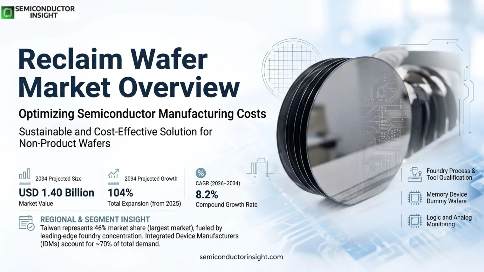
Reclaim Wafer market is valued at USD 687.1 million in 2025 and is projected to reach USD 1.40 billion by 2034, representing an 8.2% CAGR during 2026–2034. The 2026 estimated market size is USD 743.5 million. Taiwan is the largest market with 46% share, supported by its high concentration of leading-edge foundry and semiconductor manufacturing capacity.
Reclaim wafers are refurbished monitor and dummy silicon wafers used for equipment checks, process conditioning, metrology calibration and non-product manufacturing steps. They are not recovered from failed production wafers. A typical reclaim cycle removes deposited films and contamination through stripping or etching, restores geometry by grinding or polishing, performs high-purity cleaning, and verifies flatness, particles and metal contamination before the wafer returns to a fab.
The economic case strengthens as wafer diameter and process complexity increase. Prime 300 mm silicon wafers carry meaningful cost, while a monitor wafer may be cycled through non-product operations many times during its useful life. Reclaiming therefore reduces fab operating cost, lowers virgin-wafer consumption and supports waste reduction without exposing saleable product wafers to unnecessary risk.
Quality requirements are rising with advanced logic and memory. Reclaim suppliers must control metallic contamination, total thickness variation, surface roughness, particle count and remaining wafer thickness after repeated processing. Advanced nodes also increase the frequency of tool monitoring and process-control steps, creating higher demand for consistent test and dummy wafers even when product-wafer output grows at a slower rate.
Segment Analysis: By Type
By type, the market is segmented into Monitor Wafers and Dummy Wafers. Dummy wafers hold about 78% share because they are extensively used for equipment setup, chamber conditioning, thermal cycling and process-flow support, while monitor wafers are used where tighter measurement and process-control requirements apply.
| Type | Fab role | Market position |
|---|---|---|
| Dummy Wafers | Dummy wafers are used for equipment conditioning, chamber seasoning, thermal runs, deposition and etch setup, mechanical handling tests and other non-product operations. They can often tolerate broader electrical specifications than prime wafers but still require controlled geometry and cleanliness. | Largest type, about 78% share. High process-step counts and frequent preventive-maintenance cycles sustain recurring consumption across logic, memory, analog and specialty fabs. |
| Monitor Wafers | Monitor wafers support process measurements such as film thickness, particles, contamination, tool matching and repeatability. They generally require tighter surface and cleanliness specifications because the wafer itself becomes part of the measurement system. | A smaller but higher-specification segment. Advanced nodes and increasingly automated process control support demand for cleaner, flatter and more consistent reclaimed monitor wafers. |
Wafer-size and reclaim-process segmentation
The market can also be segmented by wafer size and reclaim process. 300 mm wafers represent the most important growth segment because advanced logic and memory production is concentrated on 300 mm platforms. 200 mm remains important in analog, power, MEMS and mature-node fabs. Chemical stripping, controlled grinding, chemical mechanical polishing and high-purity cleaning are combined according to the wafer’s film history and remaining thickness.
| Axis | Segments | Commercial implication |
|---|---|---|
| By Wafer Size | 200 mm · 300 mm · Other Sizes | 300 mm carries the highest unit value and strongest growth because advanced foundry and memory capacity continues to expand. 200 mm remains durable in specialty semiconductor manufacturing with long equipment lifecycles. |
| By Reclaim Process | Chemical Stripping / Etching · Grinding · CMP / Polishing · High-Purity Cleaning | The process sequence must remove prior films and damage while preserving wafer thickness and flatness. Better polishing and contamination removal increase the number of useful reclaim cycles and improve supplier economics. |
Segment Analysis: By Application
By application, IDMs account for about 70% of current market demand, followed by foundries and other semiconductor manufacturers. IDMs generate large internal requirements for monitor and dummy wafers across memory, logic, analog and power production, while foundries require high volumes of non-product wafers to qualify many customer processes and tools.
| Application | Key market insight |
|---|---|
| IDM | Integrated device manufacturers combine process development and high-volume production under one organization, creating steady demand for equipment monitoring, process qualification and preventive-maintenance wafers. Memory IDMs can be especially reclaim intensive because 3D NAND and advanced DRAM involve many repeated deposition, etch and metrology steps. |
| Foundry | Foundries operate multiple technology nodes and customer products on common tool fleets. Reclaim wafers support chamber conditioning, equipment matching and process-control tasks without consuming prime product wafers. Advanced foundry investment in Taiwan, China and the United States expands this opportunity. |
| Others | Research fabs, OSAT-related wafer processes, equipment vendors and specialty semiconductor manufacturers use reclaimed wafers for tool development, process trials and non-critical handling. Volumes are lower but specifications can be highly customized. |
Regional Analysis
Taiwan leads the Reclaim Wafer market with 46% share, followed by Japan with 33% and the United States with 7%. The market is concentrated around semiconductor manufacturing clusters because reclaim logistics benefit from short transport distances and fast turnaround. Asia Pacific remains the dominant broader region, while new U.S. and European fab investments support local service expansion.
Why is reclaim-wafer capacity concentrated near fabs?
Reclaim is a service-intensive materials business. Used wafers must be collected, processed, inspected and returned with controlled traceability. A local plant can shorten cycle time, reduce transportation risk and provide faster engineering support when a customer’s film stack or cleanliness requirement changes. This favors production bases in Taiwan, Japan, China, South Korea and established U.S. semiconductor regions.
| Region | Market position | Growth outlook | Core demand | Commercial priority |
|---|---|---|---|---|
| Taiwan / Asia Pacific | Largest | High | Foundry & memory | Turnaround, advanced-node quality and 300 mm capacity |
| Japan | Second-largest country | Moderate to high | IDM, materials & equipment | Polishing precision and long-term quality |
| North America | Growing local market | High | New fabs, logic & memory | Local capacity and supply resilience |
| Europe | Specialty growth market | Moderate | Automotive, analog & power | 200/300 mm service and lifecycle support |
| Other regions | Early-stage | Selective | Future fabs and research | Local ecosystem maturity |
Competitive Landscape
Key participants include RS Technologies, Kinik, Phoenix Silicon International, Hamada Rectech, Mimasu Semiconductor Industry, GST, Scientech, Pure Wafer, TOPCO Scientific, Ferrotec, Xtek Semiconductor, Shinryo, KST World, Vatech, OPTIM Wafer Services, Nippon Chemi-Con, KU WEI TECHNOLOGY, Hua Hsu Silicon Materials, Hwatsing Technology, Fine Silicon Manufacturing, PNC Process Systems and Silicon Valley Microelectronics. The top five suppliers hold more than 74% of global market revenue.
RS Technologies holds the leading global position and states a current market share of 33% in wafer reclaim. Its production network includes Japan, Taiwan and China. The Sanbongi plant can process 340,000 12-inch wafers per month and the Tainan plant 300,000 12-inch wafers per month, supported by proprietary chemical treatment, metal decontamination and polishing technologies.
Kinik is expanding aggressively at the high end of the market. Its May 2026 investor materials state that 12-inch reclaim/test/specialty-wafer capacity reached 360,000 wafers per month in the second quarter and will rise to 400,000 from the third quarter, with new capacity dedicated to advanced-node reclaimed wafers.
Phoenix Silicon International combines reclaim, new test wafer and thinning services. The company describes itself as the global number-one reclaim-service provider and reported 2025 revenue of NT$4.509 billion. Its roadmap includes reclaim readiness and production for 2nm processes, illustrating the move toward tighter specifications in advanced-node monitoring.
Competitive tier structure
| Competitive tier | Representative companies | Competitive strengths |
|---|---|---|
| Global leaders | RS Technologies; Kinik; Phoenix Silicon International; Hamada Rectech; Mimasu | Large 300 mm capacity, direct fab relationships, advanced-node quality and global service |
| Regional specialists | GST; Scientech; Pure Wafer; TOPCO; Ferrotec; Shinryo; KST World | Regional turnaround, mature-node expertise, customized wafer sizes and specialty process support |
| China / emerging suppliers | Xtek; Hwatsing; Fine Silicon Manufacturing; PNC Process Systems; Hua Hsu | Domestic fab proximity, capacity growth and localization-driven customer qualification |
Key companies profiled
Reclaim Wafer Capacity & Processing Analysis
Capacity is defined by stripping, grinding, polishing, cleaning, metrology and inspection throughput rather than by one polishing tool. 300 mm advanced-node reclaim uses tighter contamination and flatness specifications and therefore consumes more process-control capacity per wafer. The number of times a wafer can be reclaimed also affects effective supply because each cycle removes material from the wafer.
RS Technologies and Kinik provide visible evidence of industry capacity expansion. RS Technologies reports combined large-scale 12-inch capacity in Japan and Taiwan, while Kinik is increasing 12-inch capacity to 400,000 wafers per month in 2026. These expansions support a market that grows with fab activity rather than with consumer-device shipments alone.
Process technology can expand effective capacity by increasing reclaim cycles. Minimum material removal, low-damage grinding and improved metal decontamination preserve wafer thickness and cleanliness, allowing a wafer to return to the fab more times before retirement. This lowers customer cost and reduces the number of new test wafers required.
Market Dynamics
Growth is driven by expanding 300 mm fab capacity, rising process-control intensity, higher prime-wafer cost and sustainability. Restraints include limited reclaimable-wafer supply, strict contamination specifications, wafer-thickness loss and qualification cycles. Opportunities center on advanced-node reclaim, local capacity around new fabs and data-driven inspection.
MARKET DRIVERS
Fab capacity directly expands the reclaim pool
Every operating fab consumes non-product wafers for qualification and monitoring. SEMI expects installed 300 mm capacity to continue expanding, increasing both demand for monitor wafers and the number of used wafers available for reclamation.
Advanced nodes use tighter process control
Smaller geometries, GAA transistors, advanced DRAM and high-layer-count NAND require more metrology and chamber qualification. More process-control steps increase consumption of monitor wafers even if product-wafer volumes grow more slowly.
Reclaim lowers non-product silicon cost
Prime 300 mm wafers are too valuable to consume repeatedly for tool checks when a qualified reclaimed wafer can perform the task. Reusing each wafer several times improves fab operating economics.
Circularity improves environmental performance
Reclaim extends silicon-wafer life and reduces demand for new test wafers. This lowers material consumption and waste from non-product operations, supporting semiconductor sustainability programs.
Drivers Impact Analysis
| Driver | Impact | Primary markets | Time horizon |
|---|---|---|---|
| 300 mm fab expansion | High | Taiwan, Korea, China, U.S. | Medium to long term |
| Advanced-node process monitoring | High | Leading-edge fabs | Persistent |
| Cost reduction vs. new test wafers | High | Global fabs | Persistent |
| Waste and silicon reduction | Medium | Global | Persistent |
MARKET RESTRAINTS
Not every used wafer can be reclaimed
Wafers with excessive damage, deep contamination or insufficient remaining thickness may be rejected. Supply therefore depends on the quality and history of monitor and dummy wafers returning from fabs.
Advanced nodes tighten contamination limits
Copper, particles and residues that are acceptable for a mature process may be unacceptable near leading-edge equipment. Suppliers need advanced cleaning and analytical capability, raising capital and operating cost.
Each reclaim cycle consumes material
Grinding and polishing reduce wafer thickness. Suppliers must remove enough material to restore surface quality without shortening wafer life unnecessarily. Better process control increases the number of profitable cycles.
Qualification favors established suppliers
Fabs validate reclaimed wafers for cleanliness, geometry and process compatibility. Changing provider can require extensive trials, which creates switching barriers and slows entry by new regional competitors.
Restraints Impact Analysis
| Restraint | Impact | Exposure | Time horizon |
|---|---|---|---|
| Limited suitable used-wafer supply | High | High-utilization fabs | Persistent |
| Metal / particle contamination control | High | ||
| Thickness loss over reclaim cycles | Medium to high | Repeated reclaim | Persistent |
| Customer qualification cycles | Medium | New suppliers | Medium term |
MARKET OPPORTUNITIES
Scale 2nm and advanced-node reclaim
Phoenix Silicon International’s 2nm roadmap and Kinik’s high-end capacity investment show increasing demand for reclaimed wafers that can meet tighter leading-edge specifications.
Build local plants near new fabs
U.S., European and Chinese fab regionalization creates new service clusters. A local reclaim facility can shorten turnaround, reduce freight and improve customer engineering support.
Expand 300 mm specialty services
Advanced packaging, backside processes and new monitor applications create demand for ultra-flat, coated or otherwise customized test wafers in addition to standard reclaim.
Use automated inspection and traceability
Better metrology and data tracking can classify incoming wafers, optimize material removal and predict remaining reclaim life. This improves yield and allows customers to manage monitor-wafer inventory more precisely.
Reclaim Wafer Value Chain Analysis
Used monitor / dummy wafer collection
Film removal & surface recovery
CMP, cleaning & inspection
Fab reuse
Incoming classification determines reclaim yield
Suppliers inspect wafer thickness, breakage, film type and contamination before processing. Accurate classification avoids spending chemicals and polishing capacity on wafers that cannot meet final specifications.
Film removal must protect the silicon substrate
Different deposition stacks require different chemical or mechanical removal methods. Excessive etching damages thickness, while incomplete stripping creates contamination risk. Supplier know-how is therefore highly process specific.
Polishing and cleaning create the saleable product
Mirror finish, flatness and low metals are restored through grinding, CMP and cleaning. Metrology verifies particles, geometry and surface condition before the wafer is shipped back to the customer.
Repeated fab reuse closes the circular loop
The economic value comes from returning the same silicon wafer to non-product service multiple times. Minimum-removal technology increases the number of reclaim cycles and lowers the customer’s cost per use.
Recent Developments in the Reclaim Wafer Market
Kinik raises 12-inch reclaim/test/specialty-wafer capacity
Kinik’s first-quarter investor presentation states that 12-inch capacity reached 360,000 wafers per month in 2Q 2026 and will increase to 400,000 per month from 3Q 2026, with new capacity focused on advanced-node reclaimed wafers.
RS Technologies details global reclaim expansion
The 2025 annual report identifies wafer reclaim as the group’s core business, reports 33% current market share and outlines continued production expansion in Japan, Taiwan and China.
Phoenix Silicon International outlines 2nm reclaim roadmap
PSI’s investor presentation lists 2nm reclaim readiness in 2025 and reclaim production for 2nm in 2026, alongside test-wafer and advanced-packaging process expansion.
Kinik supplies 8-inch and 12-inch reclaimed wafers
Kinik’s current product portfolio uses ductile-mode grinding to reduce surface damage and chemical contamination compared with traditional lapping.
REPORT SCOPE & SEGMENTATION
| Attribute | Details |
|---|---|
| Study Period | 2020–2034 |
| Base Year | 2025 |
| Estimated Year | 2026 |
| Forecast Period | 2026–2034 |
| Historical Period | 2020–2025 |
| Market Size 2025 | USD 687.1 million |
| Market Size 2034 | USD 1.40 billion |
| Growth Rate | 8.2% during 2026–2034 |
| Unit | Value (USD Million/Billion) and reclaimed-wafer shipments |
| By Type | Monitor Wafers · Dummy Wafers |
| By Application | IDM · Foundry · Others |
| By Wafer Size | 200 mm · 300 mm · Other Sizes |
| By Reclaim Process | Chemical Stripping / Etching · Grinding · CMP / Polishing · High-Purity Cleaning |
| By Region | Each region analysed by wafer type, application, wafer size, reclaim process and country manufacturing ecosystem North AmericaUnited States, Canada, Mexico EuropeGermany, France, Italy, United Kingdom and other European markets Asia PacificTaiwan, Japan, China, South Korea, Singapore and other Asian markets South AmericaBrazil, Argentina and other South American markets Middle East & AfricaIsrael, Saudi Arabia, UAE, South Africa and other MEA markets |
| Key Companies Profiled | RS Technologies · Kinik · Phoenix Silicon International · Hamada Rectech · Mimasu Semiconductor Industry · GST · Scientech · Pure Wafer · TOPCO Scientific · Ferrotec · Xtek Semiconductor · Shinryo · KST World · Vatech · OPTIM Wafer Services · Nippon Chemi-Con · KU WEI TECHNOLOGY · Hua Hsu Silicon Materials · Hwatsing Technology · Fine Silicon Manufacturing · PNC Process Systems · Silicon Valley Microelectronics |
| Customization Scope | Free report customization equivalent to up to four analyst working days with purchase. Addition or alteration to country, regional and segment scope. |
Frequently Asked Questions
What is the 2025 size of the Reclaim Wafer market?
The market is valued at USD 687.1 million in 2025 and is projected to reach USD 1.40 billion by 2034. The 2026 estimate is USD 743.5 million and the 2026–2034 CAGR is 8.2%, supported by expanding fab capacity and greater process-control intensity.
Which reclaim-wafer type leads the market?
Dummy wafers lead with about 78% share because fabs use large quantities for chamber conditioning, equipment setup, maintenance and non-product process runs. Monitor wafers are a smaller, tighter-specification segment used for metrology and process-control measurements.
Which application is the largest?
IDMs account for about 70% of current demand. Vertically integrated memory, logic, analog and power manufacturers operate large tool fleets and consume monitor and dummy wafers continuously for process qualification and control.
Which country leads the market?
Taiwan leads with 46% share, followed by Japan at 33% and the United States at 7%. Taiwan’s leading position reflects its dense advanced-foundry and semiconductor-manufacturing base and strong local reclaim-service ecosystem.
What is the estimated market size in 2026?
The 2026 market size is USD 743.5 million. Growth is driven by higher 300 mm fab activity, more advanced-node process monitoring and the economic benefit of reusing silicon wafers instead of consuming new prime or test wafers.
Why are reclaimed wafers used in fabs?
They provide a lower-cost wafer for equipment monitoring, chamber seasoning, process development and tool qualification. These tasks need controlled wafer geometry and cleanliness but do not justify using a new prime wafer that could be reserved for revenue-producing devices.
What are the main market restraints?
The main restraints are limited supply of suitable used wafers, metal and particle contamination requirements, thickness loss after repeated polishing and long fab qualification cycles for new reclaim suppliers.
Why is 300 mm reclaim growing?
Advanced logic, memory and foundry manufacturing is increasingly concentrated on 300 mm wafers. New 300 mm capacity therefore creates more non-product wafer demand, while the high value of prime 300 mm silicon makes reclaim economics especially attractive.
How does reclaim support sustainability?
Reclaim extends the useful life of silicon monitor and dummy wafers, reducing virgin material consumption and waste from non-product fab operations. Better polishing technology can increase the number of reuse cycles before a wafer becomes too thin.
What does the report cover?
The report covers monitor and dummy wafers; IDM, foundry and other applications; 200 mm, 300 mm and other sizes; stripping, grinding, polishing and cleaning processes; five global regions; capacity analysis; and the major reclaim-wafer suppliers.
Research Sources & Evidence Base
View primary and authoritative evidence used in this overview
- RS Technologies. Annual Report 2025 – Wafer Reclaim Business – Primary company evidence on market share, Japan/Taiwan capacity, production bases and growth strategy.
- RS Technologies. Reclaimed Wafers – Official process information covering stripping, polishing, cleaning, copper removal and repeated reclaim.
- Kinik. Reclaimed Wafer – Official product information on 8-inch and 12-inch reclaimed wafers and ductile-mode grinding.
- Kinik. 1Q 2026 Investor Meeting – Primary evidence on 12-inch capacity expansion to 400,000 wafers per month.
- Phoenix Silicon International. Wafering Service – Official description of 6-inch, 8-inch and 12-inch reclaim-wafer services and processing technology.
- SEMI. 300mm Fab Outlook – Q2 2026 – Industry evidence on global 300 mm capacity, AI-driven fab investment and the expanding installed manufacturing base.
Get Sample Report PDF for Exclusive Insights
Report Sample Includes
- Table of Contents
- List of Tables & Figures
- Charts, Research Methodology, and more...
 Download Sample Report PDF