Key Statistics
Key Takeaways
- Polished 300mm wafers remain the commercial volume anchor, with the source page assigning them 67% of market share in 2023. Their scale reflects broad use across memory and logic manufacturing, while epitaxial and SOI variants command more application-specific value where surface engineering, device isolation, power efficiency or RF performance justify additional processing.
- Memory is the largest application, representing 52% of the market in the source-page segmentation, while Logic/MPU is positioned for faster strategic growth as AI accelerators, high-performance computing and advanced-node processors expand. SEMI’s 2025 wafer data specifically identified strong demand for polished wafers used in high-bandwidth memory and advanced epitaxial wafers used in logic.
- Asia Pacific is the largest regional market and production ecosystem. Japan remains the source page’s largest producing country, while China is identified as the fastest-growing production market. Taiwan, South Korea and Singapore add major fab demand, creating a dense local qualification network between wafer suppliers, memory manufacturers, foundries and integrated device manufacturers.
- Supply security is changing capacity geography. GlobalWafers opened an advanced integrated 300mm facility in Texas in 2025 and launched FAB300 in Italy later that year, while Japan’s METI approved a revised SUMCO supply-security plan in March 2026. These projects reduce dependence on concentrated East Asian supply without eliminating the region’s scale advantage.
- Qualification time and utilization economics remain the principal structural restraints. A new 300mm wafer line requires large crystal-growth, slicing, polishing, epitaxy, metrology and cleanroom investment, then customer-specific qualification before meaningful high-volume revenue. Siltronic’s Singapore ramp illustrates why new capacity can take several years to become fully productive even after the physical fab is commissioned.
300mm Silicon Wafers Market Overview
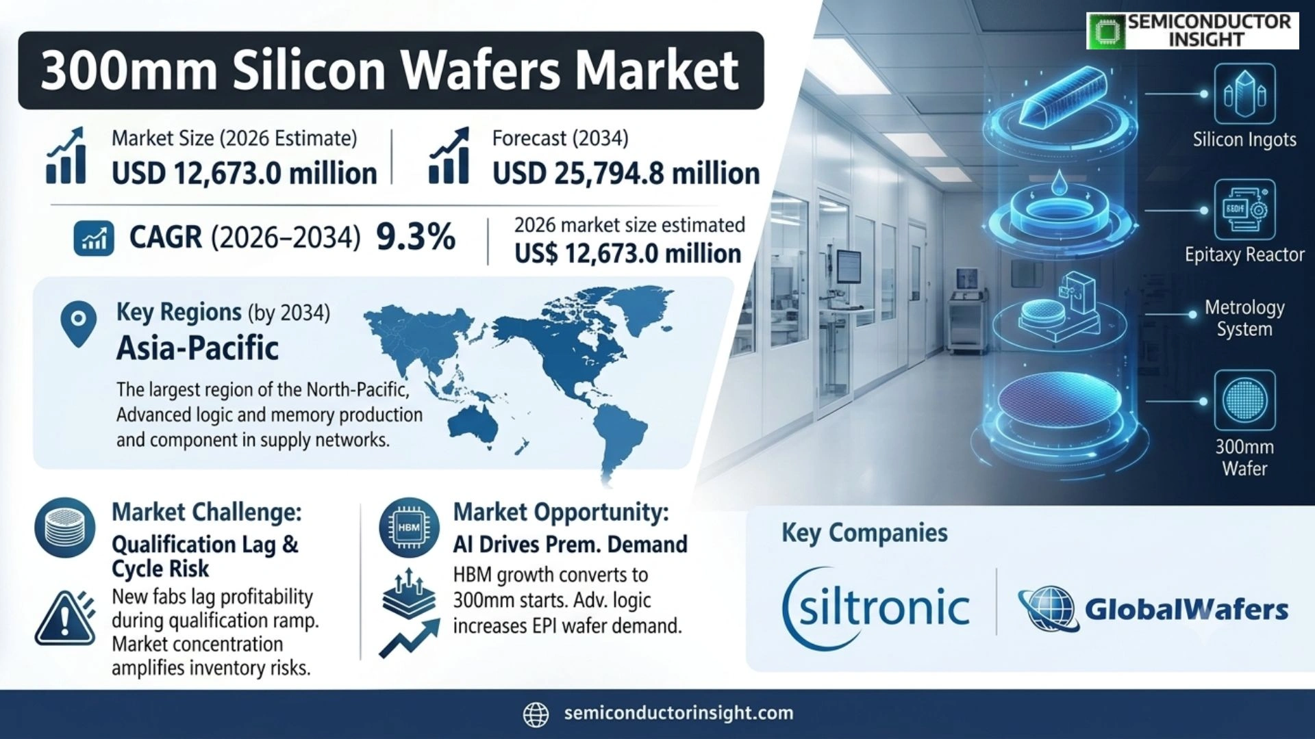
300mm Silicon Wafers Market is estimated at USD 11,595.7 million in 2025 and USD 12,673.0 million in 2026, and is projected to reach USD 25,794.8 million by 2034, implying a 9.3% CAGR during 2026–2034. Asia Pacific is the largest market because the region combines the dominant wafer-manufacturing base with the world’s largest concentration of memory, logic, foundry and integrated-device manufacturing capacity.
A 300mm silicon wafer, also called a 12-inch wafer, is the ultra-flat single-crystal silicon substrate on which hundreds or thousands of semiconductor die are fabricated. The 300mm format is the economic standard for high-volume memory and leading or mature logic production because its surface area allows substantially more die per processed wafer than 200mm formats, spreading lithography, deposition, etch and metrology cost across more devices while supporting increasingly complex process flows.
The market covered here includes polished silicon wafers, epitaxial wafers, annealed wafers and silicon-on-insulator wafers in 300mm diameter, with downstream demand segmented into memory, Logic/MPU and other device categories. It excludes smaller-diameter silicon wafers and compound-semiconductor substrates. Within this scope, commercial value is determined not only by wafer area but by crystal quality, defectivity, resistivity control, surface flatness, epitaxial specifications, SOI layer characteristics and the lengthy qualification demanded by each semiconductor manufacturer.
The demand mechanism is unusually tied to semiconductor fab capacity rather than electronics unit shipments alone. A fab establishes a qualified wafer recipe and supplier set for each device family, and changing material after production begins can require expensive requalification. That makes design-in position, consistent crystal genealogy, statistical process control and guaranteed supply more commercially important than spot-market pricing. High-end wafers therefore behave like a strategic process material with long customer relationships rather than a commodity sheet of silicon.
The market is changing now because AI infrastructure is lifting demand for advanced logic and high-bandwidth memory at the same time governments are financing geographic diversification of semiconductor supply chains. SEMI reported worldwide silicon wafer shipments rose 5.8% in 2025 to 12,973 million square inches while revenue fell 1.2% to USD 11.4 billion, showing a recovery in physical demand alongside persistent pricing and mix pressure. The combination creates opportunity for qualified capacity, but not necessarily uniform pricing power across every wafer grade.
Segment Analysis: By Type
By type, the market is segmented into 300mm polished silicon wafers, 300mm epitaxial silicon wafers, 300mm annealed silicon wafers and 300mm SOI silicon wafers. Polished wafers are the largest segment, supported by the source page’s 67% share indication for 2023, while epitaxial and SOI products capture higher-value demand where engineered surface layers or electrical isolation materially improve device performance.
| Type | Technical role | Market position and commercial logic |
|---|---|---|
| 300mm Polished Silicon Wafer | The prime wafer is sliced from a grown monocrystalline ingot, ground, chemically treated and polished to extremely tight flatness and surface-defect specifications before shipment to the device maker. | Largest type. The source page assigns polished wafers 67% share in 2023. Volume is anchored by memory and broad logic manufacturing because the product is the standard starting surface for many high-volume process flows. Competition centers on defect density, flatness, resistivity uniformity, customer yield performance and dependable delivery rather than on simple dimensional compliance. |
| 300mm Epitaxial Silicon Wafer | A precisely controlled single-crystal silicon layer is grown on the substrate after polishing. Device makers specify layer thickness, dopant concentration and defect behavior to match transistor architecture and electrical performance requirements. | Higher-value growth segment. SEMI highlighted strong 2025 demand for advanced epitaxial wafers used in logic. Epi demand benefits as advanced logic, power-management and specialty devices require more tightly engineered starting surfaces. The commercial barrier is high because crystal quality and epitaxial deposition must remain stable across millions of wafers after qualification. |
| 300mm Annealed Silicon Wafer | High-temperature treatment alters near-surface oxygen and defect characteristics, helping manufacturers optimize the wafer for specific device processes while retaining the basic 300mm monocrystalline platform. | Specification-led niche. Annealed products serve device flows where defect engineering and oxygen behavior are important. The segment is smaller than polished wafers, but its economics are less commodity-like because customers purchase a controlled material state rather than only surface finish. Supplier position depends on repeatability, technical support and long-term process compatibility. |
| 300mm SOI Silicon Wafer | A thin device-quality silicon layer is electrically isolated from the bulk substrate by a buried oxide layer. The architecture supports lower parasitic capacitance, isolation and specialized RF, automotive, aerospace and computing use cases. | Strategic specialty segment. SOI volumes are lower than mainstream polished wafer demand but can carry higher value per wafer. The U.S. Department of Commerce specifically identified 300mm SOI expansion in Missouri as strategically relevant for defense and aerospace, illustrating how resilience and application criticality can matter as much as total unit volume. |
How does wafer value differ by processing intensity?
Average selling value rises as the supplier adds more process engineering and tighter specifications. A standard polished wafer carries the broadest volume and faces the greatest exposure to utilization cycles and procurement benchmarking. Epitaxial, annealed and SOI variants embed additional processing, metrology and customer-specific requirements, so value capture shifts toward technical performance, qualification history and yield contribution. This is why a supplier can increase high-value product mix even when total square-inch demand grows more slowly.
Segment Analysis: By Application
By application, the source scope divides demand into Memory, Logic/MPU and Others. Memory is the largest segment, with a 52% source-page share for 2023, while Logic/MPU represented 46% and is strategically supported by AI and high-performance computing. The mix matters because memory buyers emphasize enormous repetitive volumes, whereas advanced logic increasingly pulls high-specification epitaxial and defect-controlled substrates.
| Application | Demand characteristics |
|---|---|
| Memory | Largest application. DRAM, NAND and high-bandwidth memory manufacturing consumes substantial 300mm polished-wafer volume because each memory generation is produced at enormous scale. AI has strengthened the premium end of this demand through HBM, and SEMI specifically cited polished wafers for HBM as a source of 2025 shipment growth. Procurement emphasizes stable long-run supply, low defectivity and cost per yielded die across very large wafer starts. |
| Logic/MPU | Logic and microprocessor demand is increasingly shaped by AI accelerators, CPUs, GPUs, networking silicon and advanced foundry nodes. The source page assigns the category 46% share in 2023 and identifies it as a rapid-growth area. Advanced logic places exceptional demands on surface cleanliness, flatness and epitaxial control, creating a pathway for higher-value wafers even when total device units do not rise at the same rate as compute intensity. |
| Others | The residual category includes analog, mixed-signal, power-management, image-sensor and other 300mm device families that have migrated from smaller diameters when volume and process economics justify conversion. These applications diversify wafer demand because their cycles do not perfectly overlap with memory or leading-edge logic. However, qualification and fab-conversion economics mean migration happens gradually rather than simply because a 300mm line offers more usable surface area. |
Regional Analysis
Asia Pacific is the largest 300mm silicon wafer market and production ecosystem, while China is the fastest-growing production market within the region. North America and Europe are increasing local wafer capacity for resilience, but Asia Pacific retains the deepest combination of wafer suppliers, advanced fabs, memory manufacturers, foundries and customer qualification infrastructure.
How does regional demand differ across the 300mm silicon wafer market?
Regional demand differs according to where semiconductor wafers are manufactured, where device fabs consume them and how aggressively governments are reducing geographic concentration. Asia Pacific combines the largest installed base with new fab construction. North America is rebuilding domestic starting-material capability around a rapidly expanding fab cluster. Europe is linking material localization with strategic autonomy. South America is policy-led and import dependent, while the Middle East and Africa remain ecosystem-development markets rather than established 300mm production centers.
| Region | Position | Growth outlook | Demand profile | What decides supplier selection |
|---|---|---|---|---|
| Asia Pacific | Largest market and production base | Highest absolute capacity growth | Integrated supplier-fab ecosystem | Qualification history, scale, defect control, local delivery, long-term agreements and the ability to support advanced memory and logic ramps across Japan, Taiwan, South Korea, China and Singapore. |
| North America | Large fab demand; historically import dependent | Accelerating localization | Reshoring and new-fab led | Domestic availability, CHIPS-aligned supply security, technical qualification with leading U.S. fab projects, traceability and the ability to meet advanced logic, memory and specialty SOI specifications. |
| Europe | Established niche production and strategic fab base | Moderate with resilience upside | Automotive, industrial and sovereignty led | High-quality local production, customer proximity, energy and sustainability performance, supply continuity, and qualification with European fabs serving automotive, industrial, power and advanced computing applications. |
| South America | Small, import-dependent base | Emerging policy support | Electronics and industrial demand led | Landed cost, import reliability, supplier technical support and whether Brazil’s semiconductor incentives eventually create enough wafer-processing scale to justify more direct regional material relationships. |
| Middle East & Africa | Nascent | Long-term ecosystem opportunity | Investment and capability-building led | Partnerships, technical training, access to global supply, government-backed semiconductor initiatives and credible downstream wafer-fab demand rather than near-term merchant 300mm production scale. |
Competitive Landscape
Competition in 300mm silicon wafers is highly concentrated because scale alone is insufficient: a supplier must combine crystal-growth expertise, polishing and epitaxy capability, ultra-low defectivity, customer-specific qualification and the financial capacity to invest through semiconductor cycles. The source page identifies Shin-Etsu Chemical, SUMCO, GlobalWafers, Siltronic and SK Siltron as the top five manufacturers with about 85% combined share in 2023.
The five global leaders compete through multi-site supply, technology breadth and long qualification histories. Device makers are reluctant to change a substrate after a process flow is qualified because seemingly small changes in crystal defects, oxygen concentration, edge geometry or surface condition can alter yield. This creates a powerful incumbency advantage: once a wafer specification is approved, purchasing negotiations focus heavily on supply assurance, capacity allocation and long-term pricing rather than on rapid supplier substitution.
Capacity strategy is increasingly geographic. GlobalWafers has added integrated capacity in the United States and Italy, while Siltronic’s Singapore fab broadens high-end 300mm and epitaxial output. SUMCO’s Japan expansion is explicitly linked to national supply security. These moves show that the competitive objective is no longer simply lowest manufacturing cost; suppliers also sell resilience, proximity and the ability to offer qualified second-source geography for customers concerned about concentrated Asian supply.
Chinese suppliers represent the most important long-term competitive change. The source page lists NSIG, Zhonghuan, Jinruihong, CCMC, GRINM, AST and ESWIN among local producers but estimates the group’s share at only about 4.2% in the referenced period. Their opportunity is substantial because Chinese fabs seek domestic materials, yet the technical barrier is equally substantial: moving from acceptable wafers to stable high-volume yield at advanced customer specifications requires years of process learning and qualification.
The market therefore has two simultaneous competitive layers. Global leaders defend advanced and high-volume programs with process stability, LTAs and multi-region capacity, while emerging suppliers target localization, mature specifications and domestic customer qualification. The result is not immediate commoditization but gradual segmentation by wafer grade, process sensitivity and geopolitical sourcing preference. Higher-value engineered wafers should remain less price elastic than mainstream polished volume.
| Competitive tier | Representative participants | What differentiates the tier |
|---|---|---|
| Tier 1 – global qualified leaders | Shin-Etsu Chemical; SUMCO; GlobalWafers; Siltronic AG; SK Siltron | Global scale, advanced crystal and polishing know-how, broad 300mm customer qualifications, long-term agreements, large capital programs and multi-site resilience. These suppliers are positioned for the most demanding memory and logic programs where wafer variability can materially affect yield. |
| Tier 2 – regional / specialist suppliers | FST Corporation; Wafer Works Corporation; MCL Electronic Materials | More focused geographic or product exposure, with opportunities in qualified niche programs, mature specifications and selected high-value applications. The commercial challenge is earning enough reference qualifications to overcome customer reluctance to change a critical starting material. |
| China localization cohort | National Silicon Industry Group (NSIG); Zhonghuan Advanced Semiconductor Materials; Zhejiang Jinruihong Technologies; Hangzhou Semiconductor Wafer (CCMC); GRINM Semiconductor Materials; Nanjing Guosheng Electronics; Hebei Puxing Electronic Technology; Shanghai Advanced Silicon Technology (AST); Zhejiang MTCN Technology; Xi’an ESWIN Material | Domestic demand and policy support create a large addressable opportunity. The decisive milestones are advanced customer qualification, sustained yield, high-specification product mix and economically utilized capacity rather than announced nameplate output alone. |
Companies profiled in the source scope
Shin-Etsu Chemical; SUMCO; GlobalWafers; Siltronic AG; SK Siltron; FST Corporation; Wafer Works Corporation; National Silicon Industry Group (NSIG); Zhonghuan Advanced Semiconductor Materials; Zhejiang Jinruihong Technologies; Hangzhou Semiconductor Wafer (CCMC); GRINM Semiconductor Materials; MCL Electronic Materials; Nanjing Guosheng Electronics; Hebei Puxing Electronic Technology; Shanghai Advanced Silicon Technology (AST); Zhejiang MTCN Technology; Xi’an ESWIN Material. The list is preserved in the source page’s scope; competitive commentary distinguishes established global scale from localization-stage capacity rather than assigning unsupported supplier shares beyond those explicitly stated.
Production Capacity Analysis
300mm wafer capacity is concentrated in a small number of highly specialized plants because production begins with ultra-pure silicon crystal growth and continues through slicing, edge shaping, lapping, etching, polishing, cleaning, annealing, epitaxy or SOI processing and extensive metrology. Nameplate capacity is therefore less informative than qualified output: a new line creates commercial supply only after it consistently meets customer defect and electrical specifications.
Asia Pacific remains the center of installed capacity, with Japan as the source page’s largest producing country and important manufacturing in South Korea, Taiwan, Singapore and China. This concentration reflects cumulative process learning and the location of major semiconductor fabs. It also creates resilience concerns for U.S. and European customers, which is why GlobalWafers’ Texas and Italy projects and SUMCO’s Japan supply-security investments are strategically important despite the time required to ramp them.
The most critical physical bottleneck is not ordinary raw silicon availability but converting semiconductor-grade feedstock into uniform 300mm crystals and then processing those crystals without introducing yield-limiting defects. Crystal pulling requires long cycles and precise thermal control; polishing and epitaxy need specialized equipment and chemistry; metrology must detect extremely small defects. A capacity addition therefore ties up substantial capital before revenue and cannot be switched quickly between specifications without customer approval.
Utilization has a large effect on profitability because depreciation, energy, cleanroom operation and skilled labor continue even when wafer starts slow. Siltronic’s Singapore project illustrates this dynamic: the company invested around EUR 2 billion through 2024, then moderated ramp speed during 2024–2026 while completing qualifications. This means market supply can remain disciplined even after a new fab is physically available, because manufacturers optimize qualification timing and customer commitments rather than flood the market with unallocated volume.
Long-term agreements and customer prepayments reduce capacity risk. Siltronic disclosed that up to 80% of its Singapore capacity can be covered by LTAs, while industry leaders increasingly align expansions with anchor customers. For buyers, these agreements provide allocation security; for suppliers, they justify capital spending through downcycles. The trade-off is lower spot flexibility, which can tighten merchant availability quickly when AI, HBM or advanced logic demand accelerates faster than contracted forecasts.
Market Dynamics
The market is being pulled upward by AI, HBM, advanced logic and new 300mm fab construction, while it is constrained by capital intensity, long qualification cycles and cyclical pricing. The most important structural shift is geographic: customers and governments are willing to pay for qualified supply in the United States and Europe because the historical production base is concentrated in East Asia, but localization must still meet the same yield and cost standards as incumbent Asian plants.
Market Drivers
| Force | Direction / relative impact* | Evidence-led commercial mechanism |
|---|---|---|
| AI, HBM and advanced logic demand | High positive | SEMI’s 2025 data linked wafer shipment growth to polished wafers used for HBM and advanced epitaxial wafers used in logic. These applications require large 300mm wafer starts and increasingly sophisticated surface specifications, improving both volume and high-value product mix for qualified suppliers. |
| New 300mm fab construction | High positive | SEMI’s Q2 2026 fab outlook identifies AI, HPC, automotive and government incentives as continuing investment drivers. Each new fab creates a multi-year substrate requirement after qualification, so fab build-outs translate into durable wafer demand rather than one-time equipment orders. |
| Supply-chain localization | Medium-high positive | U.S., Japanese and European public programs are supporting local semiconductor materials and manufacturing. The commercial effect is additional geographic capacity and more second-source qualification, expanding the addressable market for suppliers that can provide equivalent quality from multiple regions. |
| Process complexity and engineered wafers | Medium positive | Epitaxial, annealed and SOI wafers capture higher value when device performance depends on engineered starting material. As process windows tighten, the economic value of stable defectivity and material control rises because a small wafer improvement can protect far more downstream processing cost. |
AI infrastructure expands both memory and logic wafer intensity
AI servers combine accelerators, high-bandwidth memory, networking silicon and large amounts of supporting logic, so a single workload can stimulate several 300mm demand streams. SEMI’s 2025 shipment commentary is important because it identifies two specific mechanisms rather than a generic AI narrative: polished wafers benefited from HBM demand and advanced epitaxial wafers benefited from logic. That mix supports suppliers with broad technology portfolios and raises the value of high-specification capacity.
Fab expansions convert equipment investment into recurring substrate demand
Unlike lithography or deposition tools that are purchased during construction, wafers are consumed every time a fab runs. Once a new 300mm fab reaches production, substrate demand repeats for the life of the line and can increase as utilization rises. SEMI’s Q2 2026 outlook therefore matters directly to wafer suppliers: capacity additions in advanced logic and memory create recurring material pull, but the supplier must engage early enough to complete qualification before the customer’s ramp.
Government-backed localization adds a resilience premium
The United States funded GlobalWafers’ Texas and Missouri projects, Japan revised a SUMCO supply-security plan in 2026, and Europe is building local semiconductor capacity under strategic autonomy programs. These actions do not remove normal cost discipline, but they change purchasing criteria by assigning explicit value to geographic diversification. Suppliers able to replicate qualified specifications across Asia, North America and Europe can therefore compete on continuity and second-source assurance in addition to price and technical performance.
Increasing device complexity raises the value of wafer quality
A 300mm wafer entering an advanced fab accumulates enormous value through dozens of process steps. Defects in the starting substrate can therefore destroy far more downstream value than the wafer’s purchase price. As transistor architectures, interconnect density and 3D memory structures become more complex, buyers place greater weight on defectivity, flatness, epitaxial uniformity and traceability. This protects technically differentiated suppliers from pure commodity pricing in the most demanding applications.
Market Restraints
| Force | Direction / relative impact* | Evidence-led commercial mechanism |
|---|---|---|
| Capital intensity and long payback | High negative | Crystal growth, polishing, epitaxy, metrology and cleanroom infrastructure require billions of dollars at leading scale. Projects generate meaningful returns only after qualification and utilization rise, so suppliers can delay ramps when market conditions weaken, limiting how quickly new competitors can enter. |
| Lengthy customer qualification | High negative | Every major device maker has process-specific material requirements. A supplier may build physical capacity but cannot sell high-volume premium wafers until customers validate yield and reliability, turning technical qualification into a multi-quarter or multi-year commercial bottleneck. |
| Semiconductor cyclicality and pricing | Medium negative | SEMI reported wafer shipments rose in 2025 while revenue declined, showing that physical recovery does not guarantee equivalent pricing recovery. High fixed costs make utilization important, so weak traditional applications can pressure margins even when AI-related demand is strong. |
| Trade and geographic concentration | Medium negative | Most advanced production remains geographically concentrated, while trade controls and industrial policy are changing sourcing decisions. Diversification reduces single-region risk over time but can also duplicate capital, increase cost and complicate qualification across multiple supply locations. |
A new wafer fab is economically exposed before it is commercially qualified
Construction completion is only the midpoint of capacity creation. Suppliers must commission equipment, establish statistical process control, produce engineering lots and pass customer-specific qualifications before premium volume ramps. Siltronic’s Singapore disclosure that key prime-customer qualifications were completed in July 2025, after the fab began commissioning in 2024, demonstrates this lag. The result is high cash absorption during ramp and a strong advantage for incumbents with already qualified lines.
Shipment recovery can coexist with revenue pressure
SEMI’s 2025 data showed a 5.8% increase in worldwide silicon wafer shipments but a 1.2% decline in revenue to USD 11.4 billion. That divergence indicates that mix and pricing remain sensitive to weak mainstream semiconductor demand even when AI-related categories are strong. Wafer suppliers therefore face a two-speed market in which advanced products support utilization while commodity or mature segments may still require disciplined pricing and inventory management.
Customer concentration amplifies cycle risk
Large memory makers, foundries and IDMs purchase enormous wafer volumes, so changes in their inventory or fab utilization can affect supplier loading rapidly. The same qualification barriers that protect incumbent suppliers also concentrate revenue among a limited set of buyers. A delayed memory ramp or reduced foundry utilization can therefore lower wafer demand faster than end-device shipments suggest, especially when customers work down substrate inventory already committed under long-term agreements.
Localization creates cost and duplication challenges
Regional wafer plants improve resilience, but they can operate at smaller initial scale or duplicate capability already available in Asia. Customers must also qualify the new location separately even when the supplier and product family are familiar. If incentives expire before utilization matures, local capacity can face a structural cost disadvantage. The successful localization model therefore depends on anchor customers, multi-year volume commitments and technical parity rather than policy support alone.
Market Opportunities
High-bandwidth memory creates a durable polished-wafer opportunity
HBM growth converts AI compute demand into repeated 300mm memory wafer starts. Suppliers benefiting most will be those already qualified at leading DRAM manufacturers and able to support high-volume polished wafers with exceptionally stable defect and flatness performance. The commercial opportunity extends beyond 2026 because HBM capacity expansions require multi-year wafer commitments, but winning share depends on being qualified before memory lines reach peak utilization.
Advanced logic expands demand for epitaxial and premium wafers
AI accelerators, CPUs, GPUs and networking silicon push process complexity and increase the value of tightly controlled starting surfaces. SEMI explicitly connected 2025 growth to advanced epitaxial wafers for logic. This creates an attractive mix opportunity for suppliers that can combine crystal growth with in-house epitaxy, advanced metrology and co-engineering support, especially as new leading-edge fabs are constructed in the United States, Taiwan and other strategic locations.
Regional second-source qualification can create share without displacing incumbents globally
The Texas and Italy expansions show a path where GlobalWafers can win local supply positions even if Asia remains the largest production base. Customers may qualify a second geography to reduce disruption exposure, creating incremental business for suppliers that can match an existing specification in a different region. The key commercial implication is that geographic redundancy can become a paid feature when it reduces logistics, policy or disaster-concentration risk.
China localization remains a large but technically gated growth pool
Chinese wafer suppliers start from a relatively small share compared with global leaders, while domestic foundry and memory investment is substantial. Successful local companies can gain share through mature specifications first and progress toward more advanced qualifications as process capability improves. The opportunity is therefore staged: capacity announcements create potential, but repeatable customer yield, high-grade product mix and stable utilization determine whether localization turns into economically durable market share.
Supply Chain Analysis
Raw material and crystal growth. Semiconductor-grade silicon is converted into large monocrystalline ingots under tightly controlled thermal and dopant conditions. The value bottleneck is process knowledge rather than commodity feedstock alone: oxygen concentration, crystal defects, resistivity uniformity and usable ingot length directly affect downstream wafer yield. Suppliers with stable crystal recipes can spread fixed costs across more saleable wafers and support demanding customer specifications.
Slicing and surface preparation. The crystal is sliced into thin discs, then edge-shaped, lapped, chemically etched and polished. Every step must preserve geometry and reduce subsurface damage because advanced lithography depends on extremely flat, clean surfaces. High-throughput polishing and metrology are therefore central to cost competitiveness. SUMCO’s disclosed smart-factory productivity gains at major 300mm plants illustrate how incremental process efficiency can avoid large capital additions while creating material profit improvement.
Engineered wafer processing. Epitaxial growth, annealing and SOI formation add technical value after basic polishing. These steps are application specific and require additional equipment, process control and customer qualification. The commercial advantage is higher differentiation: buyers are less likely to switch a wafer that is integrated into transistor performance or isolation architecture, so suppliers can defend value through technical service and proven yield rather than only through global scale.
Fab consumption and logistics. Wafers are shipped in contamination-controlled carriers to device fabs, where they become the starting material for hundreds of process steps. Logistics reliability matters because a front-end fab cannot substitute an unqualified wafer during a shortage. Long-term agreements, local inventory, multi-region manufacturing and traceability therefore form part of the product proposition. Regional plants in Texas and Italy are strategically valuable because they shorten supply lines while providing qualified geographic redundancy.
Recent Developments in the 300mm Silicon Wafers Market
- 27 March 2026 APPROVED
Japan’s METI revised SUMCO’s supply-security plan for high-precision 300mm silicon wafers, covering crystal and processing capacity in Yamagata and Saga. The plan states required funding of ¥58 billion with a maximum ¥19.3 billion subsidy and supply milestones through 2031. This reinforces Japan’s ability to defend its upstream leadership while customers diversify semiconductor manufacturing geographically. Source - 10 February 2026 REPORTED
SEMI reported that worldwide silicon wafer shipments increased 5.8% in 2025 to 12,973 million square inches while revenue declined 1.2% to USD 11.4 billion. The organization highlighted advanced epitaxial wafers for logic and polished wafers for HBM as areas of strength, confirming that AI-related demand is improving mix even while traditional applications and pricing remain softer. Source - 16 October 2025 OPENED
GlobalWafers launched FAB300 in Novara, Italy, describing it as a fully integrated 300mm silicon wafer manufacturing facility. The project adds a new European source of advanced wafer capacity and supports regional semiconductor resilience. For customers, the commercial importance lies in the possibility of qualifying local material supply rather than relying exclusively on established East Asian production centers. Source - 16 May 2025 OPENED
GlobalWafers America officially opened its advanced integrated 300mm wafer facility in Sherman, Texas and stated an intention to expand as market demand develops. The site establishes a domestic U.S. manufacturing path for advanced 300mm wafers and aligns upstream substrate supply with major foundry and IDM investments occurring across the country. Source - 17 December 2024 FUNDED
The U.S. Department of Commerce finalized up to USD 406 million in CHIPS funding for GlobalWafers projects in Texas and Missouri. The Texas project is the first advanced high-volume 300mm silicon wafer facility in the United States, while Missouri expands 300mm SOI production. The awards illustrate how supply resilience is now an explicit capacity driver alongside conventional market demand. Source
Report Scope & Segmentation
| Attribute | Scope |
|---|---|
| Market | 300mm Silicon Wafers Market. The scope covers 300mm or 12-inch semiconductor silicon substrates used as starting material for integrated-circuit fabrication, including polished, epitaxial, annealed and silicon-on-insulator variants. Smaller silicon wafer diameters and compound-semiconductor substrates are outside the formal market definition. |
| Base / Estimated / Forecast | Base year 2025: USD 11,595.7 million. Estimated year 2026: USD 12,673.0 million. Forecast year 2034: USD 25,794.8 million. The implied CAGR for 2026–2034 is 9.3%, derived from the source page’s USD 10,610 million 2024 and USD 19,760 million 2031 anchors. |
| By Type | 300mm Polished Silicon Wafer; 300mm Epitaxial Silicon Wafer; 300mm Annealed Silicon Wafer; 300mm SOI Silicon Wafer. These labels are preserved from the source-page formal segmentation even where the descriptive overview uses shorter product names. |
| By Application | Memory; Logic/MPU; Others. The source page separately states that Memory represented 52% and Logic 46% in 2023, providing an orientation to the demand mix while the formal article avoids inventing an unsupported share for the residual category. |
| Regions | North America; Europe; Asia Pacific; South America; Middle East & Africa. Asia Pacific is treated as the largest regional market because the source page’s regional analysis says the region dominates, while Japan is separately described as the largest producing country and China as the fastest-growing production market. |
| Companies Profiled | Shin-Etsu Chemical; SUMCO; GlobalWafers; Siltronic AG; SK Siltron; FST Corporation; Wafer Works Corporation; National Silicon Industry Group (NSIG); Zhonghuan Advanced Semiconductor Materials; Zhejiang Jinruihong Technologies; Hangzhou Semiconductor Wafer (CCMC); GRINM Semiconductor Materials; MCL Electronic Materials; Nanjing Guosheng Electronics; Hebei Puxing Electronic Technology; Shanghai Advanced Silicon Technology (AST); Zhejiang MTCN Technology; Xi’an ESWIN Material. |
| Customization Scope | Free report customization equivalent to up to four analyst working days with purchase, including addition or alteration of country, regional and segment scope where the requested change remains consistent with the underlying market definition and available evidence. |
Frequently Asked Questions
What is the current size of the 300mm silicon wafers market?
The global market is estimated at USD 11,595.7 million in 2025 and USD 12,673.0 million in 2026. Using the source page’s published USD 10,610 million 2024 and USD 19,760 million 2031 anchors produces a projected USD 25,794.8 million by 2034 and an internally consistent 9.3% CAGR during 2026–2034. The source page prints 9.5%, but its two size anchors imply about 9.3%, so the anchor-based series is used.
Which region leads the 300mm silicon wafers market?
Asia Pacific is the largest regional market because it combines the dominant global wafer production base with the largest concentration of memory, foundry and advanced logic manufacturing. Within the region, Japan is identified by the source page as the largest producing country at roughly 35% of production, while China is the fastest-growing production market. Taiwan, South Korea and Singapore add substantial downstream fab and high-specification wafer capacity.
Which type of 300mm silicon wafer has the largest share?
300mm polished silicon wafers are the largest product type, with the source page indicating about 67% market share in 2023. Their leadership comes from broad use as the standard starting substrate for memory and logic manufacturing. Epitaxial, annealed and SOI wafers are smaller in volume but can capture greater value per wafer when engineered surface layers, defect characteristics or electrical isolation are critical to device performance.
What is the largest application for 300mm silicon wafers?
Memory is the largest formal application segment, with the source page assigning it 52% share in 2023, compared with 46% for Logic/MPU. AI infrastructure strengthens both categories: high-bandwidth memory consumes large volumes of polished wafers, while accelerators, CPUs and networking devices support advanced logic demand. SEMI’s 2025 industry data specifically identified HBM polished wafers and advanced logic epitaxial wafers as sources of shipment strength.
Why are 300mm wafers preferred for high-volume semiconductor manufacturing?
The 300mm diameter provides substantially more usable surface area than 200mm wafers, allowing fabs to process more die through many costly manufacturing steps at once. The economic advantage is strongest where semiconductor volumes and capital intensity justify the specialized equipment. However, wafer size alone does not determine value: advanced fabs also require extremely tight flatness, defectivity, resistivity and surface specifications, making material quality and customer qualification central to purchasing decisions.
Who are the leading manufacturers in the 300mm wafer market?
The source page identifies Shin-Etsu Chemical, SUMCO, GlobalWafers, Siltronic AG and SK Siltron as the top five global manufacturers and attributes about 85% combined share to them in 2023. Their leadership reflects decades of crystal-growth and surface-processing expertise, large capital bases, extensive customer qualifications and global supply relationships. Chinese suppliers are expanding, but their competitive progress depends on achieving stable high-volume yield at increasingly demanding customer specifications.
What is the main growth driver for the 300mm wafer market?
The strongest demand mechanism is the combination of AI, high-bandwidth memory, advanced logic and continuing 300mm fab investment. SEMI reported higher silicon wafer shipments in 2025 and specifically linked strength to polished wafers for HBM and advanced epitaxial wafers for logic. Government-backed supply-chain diversification adds a second driver by creating new regional capacity in the United States, Europe and Japan and encouraging customers to qualify more geographically resilient supply.
What are the principal restraints on new 300mm wafer capacity?
The main restraints are capital intensity, long customer qualification cycles, semiconductor cyclicality and the difficulty of maintaining ultra-low defect levels at high volume. Building a wafer fab does not create saleable premium capacity immediately; crystal growth, polishing, epitaxy and metrology processes must stabilize and customers must validate the material in production. High fixed costs also make utilization critical, so suppliers can intentionally slow ramps when market conditions are weak.
How is supply-chain localization changing competition?
Localization is creating a second competitive dimension beyond technical performance and cost. GlobalWafers opened advanced 300mm capacity in Texas and Italy, while Japan approved additional support for SUMCO. Customers can use these sites to reduce reliance on concentrated East Asian supply, but each new geography still needs qualification. Suppliers that can reproduce the same high-quality wafer specification across multiple regions can therefore sell resilience and continuity alongside defect control and pricing.
What will shape the 300mm silicon wafers market through 2034?
Through 2034, the market will be shaped by AI server investment, HBM and advanced logic wafer starts, the pace of new 300mm fab utilization, the mix of polished versus engineered wafers, customer inventory cycles and geographic diversification of semiconductor manufacturing. Asia Pacific should remain the central production ecosystem, but U.S. and European local capacity can gain strategic share. Supplier winners will combine process quality, qualification depth, capital discipline and geographically resilient capacity.
Research Sources & Evidence Base

Get Sample Report PDF for Exclusive Insights
Report Sample Includes
- Table of Contents
- List of Tables & Figures
- Charts, Research Methodology, and more...
 Download Sample Report PDF