12 Inch Semiconductor Silicon Wafer Market, Global Outlook and Forecast 2026-2034

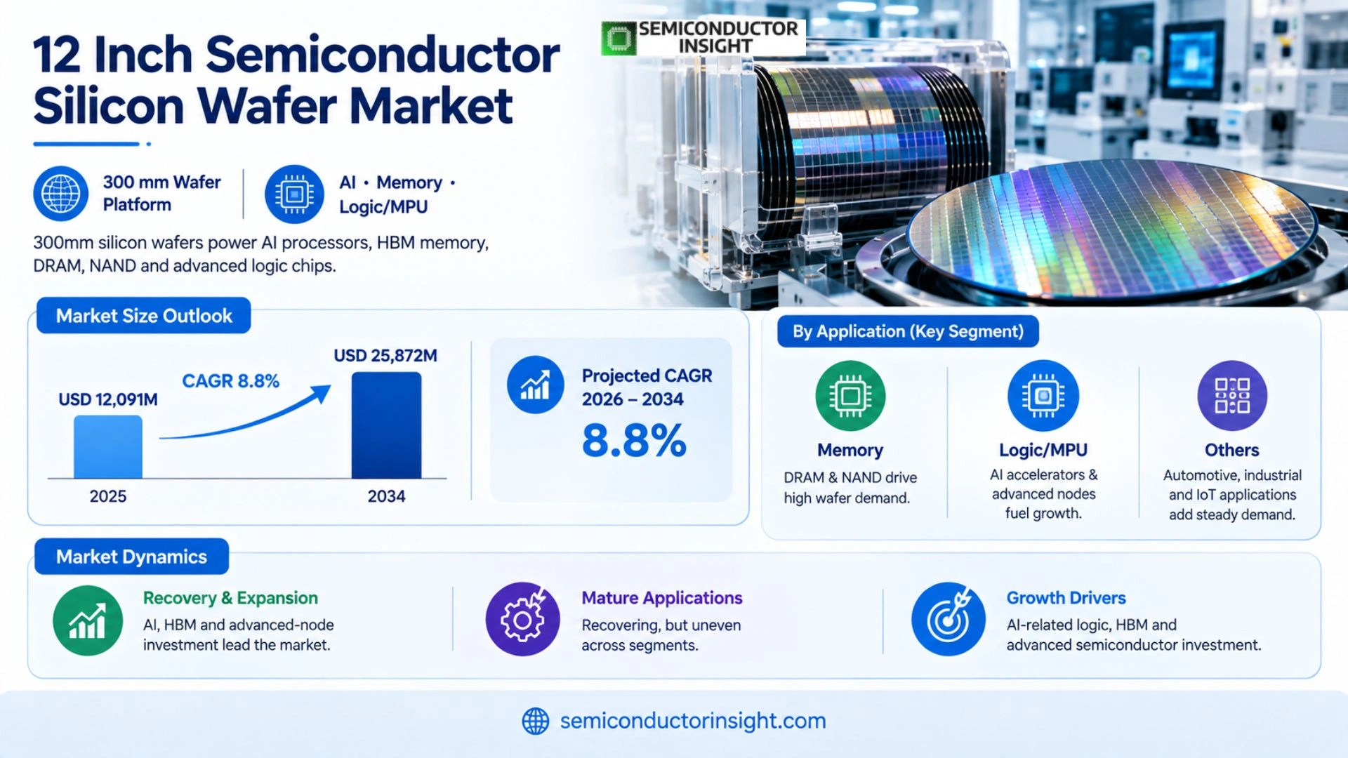
12 Inch Semiconductor Silicon Wafer Market is projected to reach approximately USD 25,872 million by 2034, implying an 8.8% CAGR for 2026–2034.

PDF Icon Download Sample Report PDF
  • Quick Dispatch

    All Orders

  • Secure Payment

    100% Secure Payment

Price range: $1,500.00 through $4,250.00

Clear

Key Statistics

2025 Market Size
USD 12,091 million
2034 Projected Size
USD 25,872 million
CAGR (2026–2034)
8.8%
Largest Market in 2025
Asia Pacific

Key Takeaways

  • USD 12.09 billion in 2025 expands to approximately USD 25.87 billion by 2034, implying an anchor-derived 8.8% CAGR.
  • 300mm polished wafers are the volume anchor, while epitaxial and SOI products capture higher-value demand where process and device requirements are more specialized.
  • AI is lifting advanced wafer demand; SEMI reported global silicon-wafer shipments of 12,973 MSI in 2025, up 5.8%, with advanced logic and HBM among the key drivers.
  • Asia Pacific dominates the supply ecosystem, combining major wafer producers with dense logic, memory and foundry manufacturing capacity.
  • Supply remains highly concentrated, making qualification, defect control, capacity discipline and multi-site resilience as important as nominal wafer price.

12 Inch Semiconductor Silicon Wafer Market Overview

12 Inch Semiconductor Silicon Wafer Market was valued at USD 12,091 million in 2025 and is projected to reach approximately USD 25,872 million by 2034, implying an 8.8% CAGR for 2026–2034. The market is centered on 300mm silicon substrates used in high-volume semiconductor manufacturing. Current demand is increasingly linked to AI-related logic, high-bandwidth memory, advanced process nodes and the broader recovery of industrial and automotive semiconductor applications, making wafer quality and reliable capacity increasingly strategic upstream constraints.

Base year: 2025 · Forecast period: 2026–2034 · Historical reference: 2019–2025 · Values in USD million unless otherwise stated; shipment data may be reported in million square inches (MSI)

A 12-inch semiconductor silicon wafer is a 300mm engineered substrate on which integrated circuits are fabricated. The wafer must provide extremely consistent geometry, surface quality, crystal characteristics and defect performance because front-end processes operate across the entire wafer surface. Larger wafer diameter also improves die economics by increasing the number of usable dies per processed wafer, which is why 300mm became the standard platform for many high-volume memory and logic applications.

The source-defined market covers 300mm Polished Silicon Wafer, 300mm Epitaxial Silicon Wafer, 300mm Annealed Silicon Wafer and 300mm SOI Silicon Wafer, with Memory, Logic/MPU and Others as applications. Each product class has a different value mechanism. Polished wafers serve the broadest manufacturing base, epitaxial wafers add controlled layers for device requirements, annealed products address thermal conditioning and SOI creates a specialized device architecture with an insulating layer. Customers qualify these materials through stringent process metrics rather than price alone.

The market is changing through a combination of technology-node migration, AI infrastructure and capacity expansion. SEMI reported worldwide silicon wafer shipments of 12,973 MSI in 2025, up 5.8% year on year, while wafer revenue declined 1.2% to USD 11.4 billion. The divergence is commercially important: volume is recovering, yet pricing remains softer in traditional semiconductor applications. In Q2 2026, shipments increased another 7.4% year on year to 3,573 MSI, indicating a strengthening demand environment led by advanced applications.

Segment Analysis: By Type

The source-defined type segmentation contains 300mm Polished Silicon Wafer, 300mm Epitaxial Silicon Wafer, 300mm Annealed Silicon Wafer and 300mm SOI Silicon Wafer. Polished wafers form the mainstream volume class, while epitaxial and engineered variants address more specific process and device requirements. The commercial difference is important: standard polished wafers compete on scale, defectivity, geometry and cost, whereas specialty products compete more heavily on process precision, technical qualification and device-specific performance.

Type Function / Definition Market Position and Demand Characteristics
300mm Polished Silicon Wafer High-purity, highly polished 300mm monocrystalline silicon wafer used as the standard starting substrate for large-scale semiconductor fabrication. Mainstream volume anchor. Polished wafers support major logic and memory manufacturing flows and therefore benefit directly from increases in wafer starts. Competition centers on defect control, flatness, surface cleanliness, thickness uniformity, lot consistency and capacity reliability. Established suppliers gain a strong benefit because fabs are reluctant to introduce wafer variability into high-cost process flows.
300mm Epitaxial Silicon Wafer 300mm silicon wafer with a controlled epitaxial layer grown on the surface to tailor electrical and device properties. A higher-value type used where layer thickness, uniformity and defect behavior are critical. AI-linked advanced logic demand has strengthened the importance of epitaxial products according to SEMI. Suppliers compete through process precision and the ability to maintain tight specifications at volume, making technical qualifications a major commercial barrier.
300mm Annealed Silicon Wafer 300mm silicon wafer subjected to controlled thermal treatment to modify or stabilize selected material properties for semiconductor processing. A specialized class serving defined process requirements rather than the broadest wafer-start base. Customers value consistency of the thermal-treatment effect and repeatability across lots. Demand depends on specific device processes, so supplier differentiation is technical and qualification led, with less exposure to pure commodity price competition than mainstream polished wafers.
300mm SOI Silicon Wafer 300mm silicon-on-insulator wafer structure with a device layer separated from the bulk substrate by an insulating layer. A specialty product used in selected logic, RF and other device architectures where electrical isolation creates system value. Demand depends on technology design rather than general wafer starts. Competition centers on layer thickness, uniformity, defect control and process compatibility, supporting higher value per wafer when customer qualification is successful.

Specification differentiation in 300mm wafers

At 300mm scale, wafer geometry and defect control are manufacturing-system variables. Small variations in thickness, flatness, particles or surface condition can influence lithography, deposition and etch uniformity and can therefore affect final device yield. SEMI’s silicon-shipment program distinguishes polished, epitaxial and other semiconductor wafer shipments, while manufacturers such as Siltronic emphasize automated production and single-wafer history tracing. The commercial implication is that wafer suppliers increasingly sell process predictability as much as physical silicon area.

The product mix is also moving toward higher-value wafers in advanced applications. SEMI reported that 2025 shipment growth was supported by strong demand for advanced epitaxial wafers used in logic and polished wafers used for HBM, while traditional semiconductor applications remained softer. This split means suppliers can experience strong shipment recovery without uniform pricing improvement. The strategic priority is therefore not only to add capacity, but to increase the share of products that solve demanding process and device requirements.

Segment Analysis: By Application

The source-defined application segmentation includes Memory, Logic/MPU and Others. Memory remains a major 300mm wafer consumer because DRAM and NAND are manufactured at scale on 300mm platforms, while logic demand is increasingly linked to AI accelerators, data-center processors and advanced foundry nodes. Current SEMI data shows a broadening recovery into industrial and automotive applications as well, creating a more diversified demand base than the market had during the weakest phase of the recent semiconductor cycle.

Application Demand Characteristics
Memory A major 300mm application with large wafer-start requirements. HBM is an important current driver because AI systems need increasingly large high-bandwidth memory capacity. The purchasing trigger is reliable high-volume wafer supply with tight surface and defect specifications. Pricing remains cyclical, so suppliers benefit when they can maintain quality and capacity utilization even as individual memory products move through pricing cycles.
Logic/MPU A critical growth application as AI accelerators, server CPUs, networking processors and advanced mobile devices move to sophisticated process nodes. Wafer quality becomes more important as process windows tighten, creating demand for low-defect polished and epitaxial products. Suppliers compete on advanced qualification, technical support and the ability to ramp consistent material alongside leading-edge fab capacity.
Others Other applications include industrial, automotive, analog, power and specialized semiconductor products that increasingly use 300mm wafers where manufacturing economics justify the format. SEMI’s 2026 shipment data indicates industrial and automotive demand is recovering, which broadens the recovery beyond AI. The segment provides diversification and helps reduce dependence on any single semiconductor end market.

12 Inch Semiconductor Silicon Wafer Market Size 2026

Regional Analysis

Asia Pacific is the largest regional market and production center because the region combines the biggest concentration of wafer suppliers with major logic, memory and foundry manufacturing ecosystems. Japan is a major wafer-production base, Taiwan anchors advanced foundry capacity, South Korea is central to memory and advanced logic, Singapore is a major 300mm manufacturing location, and China is expanding domestic wafer capacity. North America and Europe remain important strategic demand centers because of new fab investment and supply-chain localization.

How does regional demand differ across the 12 Inch Semiconductor Silicon Wafer Market?

The regional pattern follows fab location more closely than final electronics consumption. Asia Pacific converts wafer supplier capacity directly into nearby logic, memory and foundry demand. North America is increasingly project and localization led as new fabs ramp. Europe emphasizes automotive and industrial semiconductors and therefore values long-term qualification and stable supply. South America and Middle East & Africa have smaller, import-dependent demand bases. These different mechanisms affect supplier selection, inventory, technical support and capacity planning.

Region Position Growth Outlook Demand Profile Supplier-Selection Gate
Asia Pacific Largest Highest structural demand Foundry, memory and logic led Quality, capacity, qualification and proximity
North America Strategic / advanced Project-led expansion Logic, memory, automotive and new fabs Local resilience, qualification and capacity
Europe High specification Moderate / strategic Automotive and industrial Quality, long-term supply and reliability
South America Emerging Gradual Import dependent Availability, distributor support and economics
Middle East & Africa Developing Project led Semiconductor ecosystem development Partnerships, availability and technical support
Asia Pacific LARGEST

Why does Asia Pacific lead 300mm wafer demand?

Asia Pacific leads because wafer manufacturers and large semiconductor fabs are geographically interconnected. Japan anchors major wafer supply, Taiwan and South Korea provide advanced logic and memory demand, Singapore hosts a major 300mm production campus and China is expanding domestic semiconductor capacity. The concentration enables close engineering collaboration, easier logistics and high-volume customer qualification, giving the region a structural benefit that is difficult for less integrated markets to reproduce.

Market positionLargest
Growth outlookStrongest structural demand
Demand profileFoundry + memory + logic
Supplier gateQuality + qualification
Country Position in region What drives demand
Japan Major wafer supplier base Long-established wafer manufacturing and materials expertise, with customers emphasizing defect control, geometry and continuity.
Taiwan Advanced foundry hub High-volume advanced-node production drives demand for tightly controlled 300mm wafers and close supplier support.
South Korea Memory-led demand center Large DRAM and NAND ecosystems support polished-wafer demand and increasingly advanced epitaxial requirements.
Singapore Major 300mm campus Siltronic describes Singapore as its largest and most advanced production site; the second 300mm fab opened in June 2024.
China Capacity expansion zone Domestic wafer capacity is expanding alongside a large semiconductor manufacturing base, creating opportunities and competitive pressure.

Market instances

  • SEMI reported 12,973 MSI of worldwide silicon wafer shipments in 2025, up 5.8%. The increase shows that wafer demand has returned to growth, with AI-related advanced logic and HBM contributing to the recovery. The commercial implication is higher utilization across 300mm supply even though revenue remains constrained in traditional applications.
  • SEMI reported 3,573 MSI of worldwide silicon wafer shipments in Q2 2026, up 7.4% year on year. The annual increase and 9.1% quarter-on-quarter improvement indicate that AI demand is broadening beyond advanced logic and memory into power, photonics and other semiconductor applications, strengthening the overall wafer cycle.
  • Siltronic’s Singapore site exceeds 270,000 m² and includes a second 300mm fab opened in June 2024. The campus demonstrates the capital intensity, automation and history tracing required for high-volume qualified wafer production and shows why advanced wafer supply is concentrated in a limited number of sites.
  • SUMCO reported more than 10% improvement in total wafer production at a main 300mm plant. AI, data-science and IoT initiatives generated the gain, described as equivalent to more than ¥30 billion in avoided capital expenditure and more than ¥4 billion in additional annual profit. The event illustrates the importance of productivity as a capacity lever.
In the full report: Country-level market size, sales volume, manufacturer pricing, segment mix and supplier detail across the study period.
North America STRATEGIC / ADVANCED

What defines North American 300mm wafer demand?

North America is becoming more strategically important because semiconductor investment is being reshaped by new fab construction, advanced logic, memory and supply-chain localization. The region is less about historic wafer-manufacturing volume and more about securing dependable qualified material for new production capacity. Suppliers are therefore judged on technical qualification, capacity planning, logistics resilience and engineering support during fab ramps, creating opportunities for diversified global suppliers with strong customer relationships.

Market positionStrategic advanced market
Growth outlookProject-led expansion
Demand profileLogic + memory + automotive
Supplier gateResilience + qualification
Country Position in region What drives demand
United States Dominant regional demand New fabs, AI processors, memory, automotive and industrial semiconductors support expanding 300mm wafer demand.
Canada Specialized Research, industrial and advanced electronics create smaller, technically demanding demand.
Mexico Emerging downstream role Electronics and automotive manufacturing add downstream semiconductor demand but remain supplied by global wafer producers.
Rest of North America Selective Smaller fabs and electronics programs depend on qualified imported wafer supply and technical support.

Market instances

  • New North American fab projects create fresh wafer-qualification events. Every new 300mm fab must establish qualified wafer sources before high-volume production, so suppliers that can support engineering trials gain access to customer relationships that can last across multiple process generations.
  • AI infrastructure is pulling advanced logic demand higher. As AI accelerators and high-performance processors increase wafer starts, suppliers with advanced polished and epitaxial capability gain stronger relevance. The commercial opportunity is strongest for consistent quality rather than generic silicon volume.
  • Supply resilience is becoming a purchasing criterion. Customers investing in domestic semiconductor capacity increasingly value diversified wafer production, business continuity and predictable logistics. A supplier with multiple qualified sites can compete on risk reduction as well as product specifications.
  • Qualification creates switching barriers. Advanced wafers influence process yield and defect performance, so changing supplier can require substantial validation. This protects incumbents and makes technical support a core commercial capability rather than an after-sales service.
In the full report: Country-level market size, sales volume, manufacturer pricing, segment mix and supplier detail across the study period.
Europe HIGH-SPECIFICATION

What drives Europe’s 300mm wafer market?

Europe’s 300mm wafer demand is closely tied to automotive, industrial and advanced semiconductor manufacturing. Customers operate under demanding reliability and product-lifecycle requirements, so wafer consistency, traceability and long-term supply are important selection factors. The region also places strategic emphasis on semiconductor capacity localization, which creates opportunities for suppliers able to support new fabs while maintaining the quality and qualification discipline expected by automotive and industrial customers.

Market positionHigh specification
Growth outlookModerate / strategic
Demand profileAutomotive + industrial
Supplier gateQuality + long-term supply
Country Position in region What drives demand
Germany Industrial leader Automotive, industrial and power-semiconductor ecosystems require stable 300mm wafer quality and long-term supplier support.
France Advanced / research Advanced semiconductor and research activity supports specialized wafer requirements and engineering collaboration.
Italy Industrial / automotive Industrial electronics and automotive systems create demand for reliable wafer supply with consistent quality.
Benelux Advanced semiconductor ecosystem Specialized semiconductor infrastructure supports technically demanding wafer requirements and close supplier qualification.

Market instances

  • Automotive qualification increases supplier stickiness. Once a wafer grade is qualified, changing the source can affect defect behavior, process recipes and yield learning. European automotive programs therefore reward suppliers that can maintain stable material characteristics for long product cycles.
  • Engineered wafer technologies provide selective premium value. SOI and epitaxial products serve device architectures where standard polished wafers are insufficient. Suppliers can command more value when they provide tight layer control and application support rather than competing on commodity wafer price.
  • Semiconductor-capacity localization increases interest in regional supply. New European fabs can diversify customer demand even when wafer manufacturing remains internationally sourced. Suppliers that can support local qualification and logistics gain an benefit during fab ramp periods.
  • Traceability is increasingly important. Modern wafer production uses detailed process and lot records because defect analysis and yield control require precise history. Suppliers with automated tracing and mature quality systems can reduce customer process risk.
In the full report: Country-level market size, sales volume, manufacturer pricing, segment mix and supplier detail across the study period.
South America EMERGING

What shapes the South American 300mm wafer market?

South America remains a small and import-dependent market for 300mm semiconductor wafers. Brazil provides the largest electronics and industrial base, while other countries contribute demand through research, automotive, industrial and resource-linked electronics. Because local wafer production is limited, the region relies on international suppliers, making logistics, distributor relationships and customer qualification more important than local capacity economics. Opportunities are selective and tied to specific semiconductor programs rather than broad wafer-volume growth.

Market positionEmerging
Growth outlookGradual
Demand profileImport dependent
Supplier gateAvailability + economics
Country Position in region What drives demand
Brazil Largest regional base Electronics and industrial demand create the strongest local semiconductor-material opportunity.
Argentina Industrial / constrained Research and industrial electronics provide limited demand under more variable import conditions.
Chile Industrial / mining Industrial electronics and resource-sector equipment use semiconductor components but depend on global wafer supply.
Rest of South America Fragmented Demand is dispersed across smaller electronics and research activities.
Market instances

  • Import dependence makes global supplier relationships essential. Customers cannot easily substitute a qualified 300mm wafer source without validation, so established global suppliers can retain business even with longer logistics. Regional distribution and technical support can improve competitiveness significantly.
  • Industrial and automotive semiconductor recovery broadens downstream demand. SEMI’s 2026 commentary indicates recovery in these applications, creating additional wafer-start demand beyond AI and data centers. The impact is gradual because local semiconductor manufacturing remains limited.
  • Research activity can create specialty wafer demand. Development programs may use engineered or specialty 300mm structures, where technical support and reliable small-lot supply can matter more than volume pricing.
  • Working-capital requirements shape procurement. Long international lead times and minimum-order economics make inventory planning important, especially when customers are small relative to Asian or North American fab operators.
In the full report: Country-level market size, sales volume, manufacturer pricing, segment mix and supplier detail across the study period.
Middle East & Africa DEVELOPING / PROJECT-LED

Where can 300mm wafer demand develop in Middle East & Africa?

Middle East & Africa is an early-stage semiconductor-material market where demand depends on electronics manufacturing, semiconductor projects, research infrastructure and strategic technology programs. Most wafer supply is imported, so project timing, technical partnerships and logistics are critical. The region is unlikely to match Asia in volume during the near term, but individual fab or advanced-electronics projects can create concentrated opportunities for suppliers able to provide qualification support and dependable international delivery.

Market positionDeveloping
Growth outlookProject led
Demand profileSemiconductor ecosystem build-out
Supplier gatePartnership + availability
Country Position in region What drives demand
Israel Technically advanced niche Advanced semiconductor and electronics activity creates specialized demand and high technical requirements.
UAE Emerging technology hub Technology infrastructure and industrial initiatives create selective downstream demand.
Saudi Arabia Strategic development Large industrial and technology programs can create future semiconductor demand as ecosystem capacity develops.
South Africa Industrial / research Industrial and research activity provides smaller but technically relevant demand.
North Africa Emerging manufacturing Electronics assembly and export-oriented production can gradually widen semiconductor-material demand.

Market instances

  • Technology-ecosystem development is the main opportunity. A new semiconductor manufacturing or advanced-electronics project can create qualified wafer demand where none previously existed. Suppliers positioned early can establish engineering relationships before production volumes scale.
  • Technical support matters disproportionately in emerging markets. Wafer qualification requires expertise in geometry, defectivity and surface characteristics, so local engineering and application support can differentiate a global supplier even when production remains offshore.
  • Project timing makes demand lumpy. Wafer consumption can rise sharply when a new manufacturing program begins but remain small between projects. Suppliers should align capacity and inventory with concrete project milestones rather than assume steady regional volume.
  • Global suppliers remain central. Until a broader regional ecosystem develops, customers depend on established 300mm wafer manufacturers with qualified products, global logistics and process expertise. This reinforces the value of multi-site supply and strong customer engineering.
In the full report: Country-level market size, sales volume, manufacturer pricing, segment mix and supplier detail across the study period.

Competitive Landscape

The 300mm wafer market is highly concentrated because crystal growth, polishing, inspection, cleaning and customer qualification require substantial capital and process expertise. The leading group—Shin-Etsu Chemical, SUMCO, GlobalWafers, Siltronic AG and SK Siltron—competes through global capacity, advanced quality control, long customer relationships and multi-site supply. Regional suppliers compete by deepening qualifications and serving specific geographies, while emerging Chinese manufacturers emphasize localization, capacity expansion and technology catch-up.

The full company scope is Shin-Etsu Chemical, SUMCO, GlobalWafers, Siltronic AG, SK Siltron, FST Corporation, Wafer Works Corporation, National Silicon Industry Group (NSIG), Zhonghuan Advanced Semiconductor Materials, Zhejiang Jinruihong Technologies, Hangzhou Semiconductor Wafer (CCMC), GRINM Semiconductor Materials, MCL Electronic Materials, Nanjing Guosheng Electronics, Hebei Puxing Electronic Technology, Shanghai Advanced Silicon Technology (AST), Zhejiang MTCN Technology and Xi’an ESWIN Material. The companies are not equivalent in scale or qualification depth, so the report separates global leaders from regional and localization-focused suppliers rather than implying uniform competitive strength.

Qualification is the principal commercial barrier because a fab buys process predictability rather than a generic 300mm disk. Defectivity, geometry, surface quality, electrical properties, lot history and stability over time influence yield, and any change requires engineering validation. Suppliers with qualified material at leading-edge customers can therefore retain programs across multiple process generations. New entrants must demonstrate repeatability, capacity and technical service before installed capacity translates into meaningful market share.

Capacity strategy is also becoming a competitive differentiator. Siltronic’s Singapore footprint demonstrates investment in a large automated regional campus, while SUMCO’s productivity program shows how digitalization can increase effective throughput without immediate construction. Global suppliers can use multiple plants to manage regional risk, while Chinese suppliers can use domestic capacity to reduce localization barriers. The market is therefore moving toward a combination of scale, qualification, productivity and supply resilience rather than price-only competition.

Tier Companies Basis of Competition
Global leaders / diversified Shin-Etsu Chemical; SUMCO; GlobalWafers; Siltronic AG; SK Siltron High-volume 300mm capacity, advanced crystal and wafer processing, global qualifications, defect control, customer engineering and multi-site supply.
Established regional suppliers FST Corporation; Wafer Works Corporation; National Silicon Industry Group (NSIG) Regional capacity, targeted product portfolios, customer proximity and growing qualification depth.
China growth suppliers Zhonghuan Advanced Semiconductor Materials; Zhejiang Jinruihong Technologies; Hangzhou Semiconductor Wafer (CCMC); GRINM Semiconductor Materials; MCL Electronic Materials; Nanjing Guosheng Electronics; Hebei Puxing Electronic Technology; Shanghai Advanced Silicon Technology (AST); Zhejiang MTCN Technology; Xi’an ESWIN Material Localization, capacity expansion, domestic fab qualifications and movement toward higher-specification 300mm products.

Full profiled company list

The complete company list covered in the report is Shin-Etsu Chemical, SUMCO, GlobalWafers, Siltronic AG, SK Siltron, FST Corporation, Wafer Works Corporation, National Silicon Industry Group (NSIG), Zhonghuan Advanced Semiconductor Materials, Zhejiang Jinruihong Technologies, Hangzhou Semiconductor Wafer (CCMC), GRINM Semiconductor Materials, MCL Electronic Materials, Nanjing Guosheng Electronics, Hebei Puxing Electronic Technology, Shanghai Advanced Silicon Technology (AST), Zhejiang MTCN Technology and Xi’an ESWIN Material. Their competitive positions differ by wafer type, geography, process generation, qualification status and manufacturing scale.

Production Capacity Analysis / Supply-Side Analysis

300mm wafer manufacturing spans high-purity silicon, crystal growth, ingot shaping, slicing, edge treatment, lapping, polishing, cleaning, inspection and optional epitaxial or engineered-substrate processing. The supply-side challenge is not simply producing circular wafers; it is producing them at customer-qualified quality with extremely low defectivity and stable geometry. Capital equipment, clean manufacturing environments, process-control systems and long qualification cycles therefore make effective capacity more constrained than headline factory capacity.

SEMI reported worldwide silicon wafer shipments of 12,973 MSI in 2025, up 5.8%, and 3,573 MSI in Q2 2026, up 7.4% year on year. Those figures show a meaningful recovery in the wafer cycle. However, the 2025 revenue decline of 1.2% to USD 11.4 billion indicates that additional shipment area does not automatically translate into stronger pricing. Suppliers therefore need disciplined capacity management and a mix weighted toward higher-value applications.

Siltronic’s Singapore operation illustrates the physical scale of advanced wafer supply. The company describes the site as its largest and most advanced production center, with 300mm wafer and ingot manufacturing, a second 300mm fab opened in June 2024, automated production and single-wafer history tracing across more than 270,000 m². Such facilities require long planning horizons, extensive capital and customer qualification, creating meaningful barriers to rapid entry and rapid capacity substitution.

SUMCO demonstrates a second route: productivity rather than construction. The company reported more than 10% improvement in total wafer production at a main 300mm plant through AI, data science and IoT initiatives, with an associated estimate of more than ¥30 billion in avoided capital expenditure and more than ¥4 billion of additional annual profit. The supply-side implication is that digital process optimization can materially increase effective capacity when physical fab expansion would otherwise take years.

China’s expanding wafer manufacturing base creates a competitive localization pathway, but installed capacity does not immediately equal qualified capacity. Customers need reproducible defect, geometry, surface and electrical characteristics across commercial lots before a source can be considered interchangeable. The result is a gradual competitive transition in which new suppliers first win lower-risk or domestic programs and then use those references to qualify for more advanced applications and broader international demand.

Market Dynamics

The 300mm wafer market is in a recovery and expansion phase led by AI-related logic, HBM and advanced-node semiconductor investment, while mature applications recover more unevenly. The USD 12,091 million 2025 base and 8.8% CAGR imply strong structural growth, and SEMI’s shipment data confirms that the operating cycle has turned upward. Yet pricing remains differentiated, so the central commercial issue is whether suppliers can convert growing wafer starts into higher utilization and stronger value per wafer.

MARKET DRIVERS

Drivers Impact Analysis*

Factor Relative Impact Geographic Relevance Impact Timeline
AI data centers and advanced logic High Global; strongest in Asia Pacific and North America 2025–2034
HBM and advanced memory High Asia Pacific memory hubs 2025–2034
300mm advanced-node capacity High Global advanced fab regions 2026–2034
Industrial and automotive semiconductor recovery Medium Asia Pacific, Europe, North America 2026–2034

AI demand is raising advanced wafer utilization

SEMI reported that 2025 shipment growth was supported by strong demand for advanced epitaxial wafers used in logic and polished wafers used for HBM. The link to AI is commercially important because advanced logic and memory require highly consistent 300mm material. Suppliers with qualified advanced products can benefit from fab expansion even when consumer-oriented applications remain softer.

HBM increases demand for high-quality polished wafers

HBM requires substantial memory capacity and therefore creates additional wafer starts within advanced memory manufacturing. The commercial requirement is not simply more area; fabs need wafers that maintain tight surface and defect specifications. This favors suppliers with high-volume polishing, cleaning and inspection capabilities and deep customer qualification. The commercial significance is strongest when the material is qualified for a production process, because replacing a proven wafer source can introduce yield, process-control and supply-continuity risk.

Advanced process nodes increase the value of defect control

As geometries shrink, wafer-level defects, flatness variation and surface contamination can have a larger impact on yield. Customers therefore place greater value on low-defect material, repeatable geometry and lot history. Suppliers that demonstrate stable process capability can capture more value because their wafer effectively protects expensive downstream fab output. The commercial significance is strongest when the material is qualified for a production process, because replacing a proven wafer source can introduce yield, process-control and supply-continuity risk.

Automotive and industrial recovery broadens the cycle

SEMI’s 2026 updates indicated recovery in automotive and industrial semiconductor demand alongside AI strength. This matters because diversified wafer demand can improve fab utilization and reduce dependence on one end market. Automotive and industrial programs also favor established suppliers due to long qualification and product-lifecycle requirements. The commercial significance is strongest when the material is qualified for a production process, because replacing a proven wafer source can introduce yield, process-control and supply-continuity risk.

MARKET RESTRAINTS

Restraints Impact Analysis*

Factor Relative Impact Geographic Relevance Impact Timeline
High manufacturing and qualification cost Medium Global 2025–2034
Supplier concentration Medium Global 2025–2034
Mature-node pricing pressure Medium Global mature fabs Recurring
Long capacity-ramp and qualification cycles Medium New fab regions 2025–2034

Manufacturing and qualification are expensive

300mm wafer production requires high-purity materials, crystal-growth capability, precision polishing and extensive inspection. The economics are further constrained by customer qualification, which can require engineering lots and repeated process validation. New capacity therefore takes time to become revenue-producing capacity, limiting how quickly entrants can respond to market expansion or customer requests for second sources.

Supplier concentration limits interchangeability

The market is anchored by a small number of large qualified suppliers because process history and defect control are difficult to reproduce. Customers have incentives to diversify, but a second source must perform consistently before it can reduce dependence. This keeps concentration high and supports strong incumbent positions despite increasing investment by regional suppliers.

Mature-node pricing can lag shipment growth

SEMI’s 2025 results show shipment area up 5.8% while wafer revenue declined 1.2% to USD 11.4 billion. The divergence demonstrates that volume growth can be accompanied by price pressure, especially outside the strongest AI-linked segments. Suppliers therefore need mix discipline, productivity improvements and capacity management to protect returns. The commercial significance is strongest when the material is qualified for a production process, because replacing a proven wafer source can introduce yield, process-control and supply-continuity risk.

Capacity ramps require long qualification cycles

A new wafer fab or production line does not become interchangeable with an established source on opening day. Customers need to validate geometry, surface quality, defectivity and process behavior before ramping volume. This creates a lag between capital expenditure and commercial output and can make supply tight even when announced capacity appears ample.

MARKET OPPORTUNITIES

Advanced epitaxial wafers for AI logic

The strongest premium opportunity is in epitaxial products supporting advanced logic processes used for AI accelerators and high-performance computing. Suppliers can capture more value when they combine tight layer control with low defectivity and customer engineering. The commercial benefit is largest where wafer performance directly influences process yield and the product cannot be replaced with a standard polished substrate without qualification.

HBM-linked polished wafer demand

HBM growth supports additional polished-wafer demand in advanced memory fabs. Suppliers benefit when they can scale output without compromising surface quality, particles, geometry and lot consistency. Productivity programs, automation and high-throughput inspection therefore become strategic tools for capturing demand while preserving margins as overall memory cycles fluctuate. The commercial significance is strongest when the material is qualified for a production process, because replacing a proven wafer source can introduce yield, process-control and supply-continuity risk.

China localization and secondary sourcing

China’s wafer-capacity expansion offers domestic customers additional supply options and creates opportunities for suppliers to deepen qualifications. The key requirement is not installed capacity alone but repeatable product quality. Companies that convert new capacity into qualified advanced 300mm output can gain share locally and provide global customers with additional sourcing flexibility.

Automotive and industrial recovery

The gradual recovery of automotive and industrial semiconductors creates a demand stream beyond AI. Suppliers with long-term programs, stable quality and strong qualification support can benefit because these end markets value continuity and predictable material behavior. The opportunity also helps smooth utilization when consumer and memory cycles become less synchronized.

Supply Chain Analysis

Stage Value Capture and Bottleneck
UPSTREAM High-purity silicon, quartz and crucible systems, dopants and specialty chemicals feed crystal growth. Purity and contamination control affect downstream wafer quality, so upstream variation can become a major yield issue. The commercial relationship is consequently long term and quality driven, with limited tolerance for abrupt material substitution.
MANUFACTURING Crystal growth, ingot shaping, slicing, edge treatment, lapping, polishing, cleaning and inspection create the core wafer value. Epitaxial and engineered products add additional process steps. Yield, defectivity, flatness, surface quality and automation determine effective capacity, while qualification determines whether that capacity is commercially usable.
CHANNEL 300mm wafers are generally sold directly to foundries and IDMs because each customer qualifies material against specific processes. Contracts, engineering support, lot traceability and capacity planning are integral to the commercial relationship. Distribution plays a smaller role than in standard electronic components because qualification and process support are central.
DOWNSTREAM Foundries and IDMs use 300mm wafers for memory, logic, MPU, analog, power and other devices. Downstream process technology determines wafer requirements, so AI, HBM and advanced nodes can pull higher-value polished and epitaxial demand upstream while mature-node recovery sustains broader volume.

Recent Developments

  • 29 Jul 2026 Published SEMI reports 7.4% year-on-year growth in silicon wafer shipments in Q2 2026 Worldwide silicon wafer shipments reached 3,573 MSI in Q2 2026, up 7.4% year on year and 9.1% sequentially. SEMI said AI-related demand broadened beyond advanced logic and memory into power, photonics and other applications. The development confirms improving utilization across the semiconductor wafer supply chain.Source: https://www.semi.org/en/semi-press-release/semi-reports-worldwide-silicon-wafer-shipments-increase-7.4-percent-year-on-year-in-q2-2026
  • 10 Feb 2026 Published SEMI reports 5.8% growth in annual silicon wafer shipments for 2025 Worldwide silicon wafer shipments increased 5.8% to 12,973 MSI in 2025, while wafer revenue declined 1.2% to USD 11.4 billion. SEMI linked shipment strength to AI-driven demand for advanced epitaxial logic wafers and polished wafers used in HBM, while traditional applications remained weaker. The development highlights a two-speed recovery.Source: https://www.semi.org/en/semi-press-release/semi-reports-2025-annual-worldwide-silicon-wafer-shipments-and-revenue-results
  • Jun 2024 Capacity opened Siltronic opens its second 300mm fab in Singapore Siltronic states that the second 300mm fab at its Singapore site officially opened in June 2024. The company describes the site as its largest and most advanced production center, with a footprint above 270,000 m², sophisticated automation and single-wafer history tracing. The investment demonstrates the scale required to build qualified 300mm capacity.Source: https://www.siltronic.com/en/our-company/sites.html
  • 2024 Productivity milestone SUMCO reports more than 10% productivity improvement at a main 300mm plant SUMCO reported more than 10% improvement in total wafer production at a main 300mm plant through AI, data science and IoT initiatives. The company described the effect as equivalent to more than ¥30 billion of avoided capital expenditure and more than ¥4 billion in additional annual profit. The development shows the importance of digital productivity as a capacity lever.Source: https://www.sumcosi.com/english/csr/pdf/csr_rep24en.pdf

Report Scope & Segmentation

Attribute Scope
Study Period 2019–2034, using 2025 as the base year.
Base Year 2025.
Estimated Year 2025.
Forecast Period 2026–2034.
Historical Period 2019–2025.
Market Size Approximately USD 12,091 million in 2025 and USD 25,872 million in 2034.
Growth Rate 8.8% CAGR for 2026–2034 based on published market-size anchors.
Unit USD million for market value; wafer shipments are reported in MSI by SEMI.
By Type 300mm Polished Silicon Wafer; 300mm Epitaxial Silicon Wafer; 300mm Annealed Silicon Wafer; 300mm SOI Silicon Wafer.
By Application Memory; Logic/MPU; Others.
By Region North America; Europe; Asia Pacific; South America; Middle East & Africa.
Key Companies Profiled Shin-Etsu Chemical; SUMCO; GlobalWafers; Siltronic AG; SK Siltron; FST Corporation; Wafer Works Corporation; National Silicon Industry Group (NSIG); Zhonghuan Advanced Semiconductor Materials; Zhejiang Jinruihong Technologies; Hangzhou Semiconductor Wafer (CCMC); GRINM Semiconductor Materials; MCL Electronic Materials; Nanjing Guosheng Electronics; Hebei Puxing Electronic Technology; Shanghai Advanced Silicon Technology (AST); Zhejiang MTCN Technology; Xi’an ESWIN Material.
Customization Scope Country-level market size, shipment data, pricing, supplier profiling, capacity detail, application analysis and additional cuts consistent with the defined market scope.

What is the 2025 size of the 12 Inch Semiconductor Silicon Wafer Market?

The 2025 market size is approximately USD 12,091 million. The figure is derived from the published 2023 market value of USD 10,210 million and the published 2030 value of USD 18,450 million using the deterministic anchor method. It represents the defined 300mm semiconductor-silicon-wafer market, not the full global silicon or solar-wafer universe.

What is the projected market size by 2034?

The market is projected to reach approximately USD 25,872 million by 2034, corresponding to an 8.8% CAGR for 2026–2034. The outlook reflects sustained expansion in 300mm wafer consumption, driven by advanced logic, memory and specialty semiconductor capacity. Higher wafer starts increase demand for substrates, while tighter defect and flatness requirements raise the value of premium-grade material and supplier process control.

Which wafer type leads the market?

300mm Polished Silicon Wafer is the mainstream volume class because it provides the starting substrate for large-scale memory and logic manufacturing. Epitaxial, annealed and SOI wafers address narrower device and process requirements. Supplier competition therefore differs by type: polished wafers emphasize scale and defect control, while specialty wafers emphasize technical precision and qualification.

Which application leads demand?

Memory is a major 300mm wafer application because DRAM, NAND and HBM manufacturing require large wafer-start volumes. Logic/MPU is another major demand source, particularly as AI accelerators, server processors and advanced foundry nodes expand. The current market therefore depends heavily on the investment cycles of advanced memory and logic manufacturers.

What is driving 300mm wafer demand in 2026?

SEMI reported 3,573 MSI of worldwide silicon-wafer shipments in Q2 2026, up 7.4% year on year and 9.1% sequentially. SEMI linked the improvement to AI-related demand expanding beyond advanced logic and memory into power, photonics and other applications, showing that the recovery is broadening across the semiconductor ecosystem. The commercial significance is strongest when the material is qualified for a production process, because replacing a proven wafer source can introduce yield, process-control and supply-continuity risk.

Why is Asia Pacific the largest regional market?

Asia Pacific combines major wafer suppliers with the world’s largest concentration of semiconductor fabs. Japan anchors wafer manufacturing, Taiwan and South Korea serve advanced logic and memory, Singapore hosts a major 300mm production site, and China continues to expand domestic capacity. Geographic proximity supports qualification, logistics and long-term supplier relationships.

How concentrated is the 300mm wafer supplier market?

The source-defined company list is dominated by Shin-Etsu Chemical, SUMCO, GlobalWafers, Siltronic AG and SK Siltron, which form the principal global supplier tier. Concentration reflects high capital requirements, long customer-qualification cycles, defect-control expertise and the difficulty of achieving interchangeable quality at 300mm volume. The commercial significance is strongest when the material is qualified for a production process, because replacing a proven wafer source can introduce yield, process-control and supply-continuity risk.

What are the main restraints on the market?

The main restraints are high manufacturing and qualification costs, concentrated supplier capacity, long capacity-ramp cycles and mature-node pricing pressure. SEMI’s 2025 results illustrate the pricing issue because shipment area grew 5.8% while wafer revenue declined 1.2% to USD 11.4 billion. The commercial significance is strongest when the material is qualified for a production process, because replacing a proven wafer source can introduce yield, process-control and supply-continuity risk.

What role does productivity play in wafer supply?

Productivity can increase effective capacity without immediate fab construction. SUMCO reported more than 10% improvement in total wafer production at a main 300mm plant using AI, data science and IoT initiatives, equivalent to more than ¥30 billion of avoided capital expenditure and more than ¥4 billion of annual profit. Such gains improve capacity economics.

Which companies are covered in the competitive landscape?

The full company scope includes Shin-Etsu Chemical, SUMCO, GlobalWafers, Siltronic AG, SK Siltron, FST Corporation, Wafer Works Corporation, National Silicon Industry Group (NSIG), Zhonghuan Advanced Semiconductor Materials, Zhejiang Jinruihong Technologies, Hangzhou Semiconductor Wafer (CCMC), GRINM Semiconductor Materials, MCL Electronic Materials, Nanjing Guosheng Electronics, Hebei Puxing Electronic Technology, Shanghai Advanced Silicon Technology (AST), Zhejiang MTCN Technology and Xi’an ESWIN Material.

12 Inch Semiconductor Silicon Wafer Market, Global Outlook and Forecast 2026-2034

Get Sample Report PDF for Exclusive Insights

Report Sample Includes

  • Table of Contents
  • List of Tables & Figures
  • Charts, Research Methodology, and more...

PDF Icon Download Sample Report PDF

Download Sample Report

Table of Content

1 Introduction to Research & Analysis Reports
1.1 12 Inch Semiconductor Silicon Wafer Market Definition
1.2 Market Segments
1.2.1 Segment by Type
1.2.2 Segment by Application
1.3 Global 12 Inch Semiconductor Silicon Wafer Market Overview
1.4 Features & Benefits of This Report
1.5 Methodology & Sources of Information
1.5.1 Research Methodology
1.5.2 Research Process
1.5.3 Base Year
1.5.4 Report Assumptions & Caveats
2 Global 12 Inch Semiconductor Silicon Wafer Overall Market Size
2.1 Global 12 Inch Semiconductor Silicon Wafer Market Size: 2023 VS 2030
2.2 Global 12 Inch Semiconductor Silicon Wafer Market Size, Prospects & Forecasts: 2019-2030
2.3 Global 12 Inch Semiconductor Silicon Wafer Sales: 2019-2030
3 Company Landscape
3.1 Top 12 Inch Semiconductor Silicon Wafer Players in Global Market
3.2 Top Global 12 Inch Semiconductor Silicon Wafer Companies Ranked by Revenue
3.3 Global 12 Inch Semiconductor Silicon Wafer Revenue by Companies
3.4 Global 12 Inch Semiconductor Silicon Wafer Sales by Companies
3.5 Global 12 Inch Semiconductor Silicon Wafer Price by Manufacturer (2019-2024)
3.6 Top 3 and Top 5 12 Inch Semiconductor Silicon Wafer Companies in Global Market, by Revenue in 2023
3.7 Global Manufacturers 12 Inch Semiconductor Silicon Wafer Product Type
3.8 Tier 1, Tier 2, and Tier 3 12 Inch Semiconductor Silicon Wafer Players in Global Market
3.8.1 List of Global Tier 1 12 Inch Semiconductor Silicon Wafer Companies
3.8.2 List of Global Tier 2 and Tier 3 12 Inch Semiconductor Silicon Wafer Companies
4 Sights by Product
4.1 Overview
4.1.1 Segment by Type – Global 12 Inch Semiconductor Silicon Wafer Market Size Markets, 2023 & 2030
4.1.2 300mm Polished Silicon Wafer
4.1.3 300mm Epitaxial Silicon Wafer
4.1.4 300mm Annealed Silicon Wafer
4.1.5 300mm SOI Silicon Wafer
4.2 Segment – Global 12 Inch Semiconductor Silicon Wafer Revenue & Forecasts
4.2.1 Segment – Global 12 Inch Semiconductor Silicon Wafer Revenue, 2019-2024
4.2.2 Segment – Global 12 Inch Semiconductor Silicon Wafer Revenue, 2025-2030
4.2.3 Segment – Global 12 Inch Semiconductor Silicon Wafer Revenue Market Share, 2019-2030
4.3 Segment – Global 12 Inch Semiconductor Silicon Wafer Sales & Forecasts
4.3.1 Segment – Global 12 Inch Semiconductor Silicon Wafer Sales, 2019-2024
4.3.2 Segment – Global 12 Inch Semiconductor Silicon Wafer Sales, 2025-2030
4.3.3 Segment – Global 12 Inch Semiconductor Silicon Wafer Sales Market Share, 2019-2030
4.4 Segment – Global 12 Inch Semiconductor Silicon Wafer Price (Manufacturers Selling Prices), 2019-2030
5 Sights by Application
5.1 Overview
5.1.1 Segment by Application – Global 12 Inch Semiconductor Silicon Wafer Market Size, 2023 & 2030
5.1.2 Memory
5.1.3 Logic/MPU
5.1.4 Others
5.2 Segment by Application – Global 12 Inch Semiconductor Silicon Wafer Revenue & Forecasts
5.2.1 Segment by Application – Global 12 Inch Semiconductor Silicon Wafer Revenue, 2019-2024
5.2.2 Segment by Application – Global 12 Inch Semiconductor Silicon Wafer Revenue, 2025-2030
5.2.3 Segment by Application – Global 12 Inch Semiconductor Silicon Wafer Revenue Market Share, 2019-2030
5.3 Segment by Application – Global 12 Inch Semiconductor Silicon Wafer Sales & Forecasts
5.3.1 Segment by Application – Global 12 Inch Semiconductor Silicon Wafer Sales, 2019-2024
5.3.2 Segment by Application – Global 12 Inch Semiconductor Silicon Wafer Sales, 2025-2030
5.3.3 Segment by Application – Global 12 Inch Semiconductor Silicon Wafer Sales Market Share, 2019-2030
5.4 Segment by Application – Global 12 Inch Semiconductor Silicon Wafer Price (Manufacturers Selling Prices), 2019-2030
6 Sights by Region
6.1 By Region – Global 12 Inch Semiconductor Silicon Wafer Market Size, 2023 & 2030
6.2 By Region – Global 12 Inch Semiconductor Silicon Wafer Revenue & Forecasts
6.2.1 By Region – Global 12 Inch Semiconductor Silicon Wafer Revenue, 2019-2024
6.2.2 By Region – Global 12 Inch Semiconductor Silicon Wafer Revenue, 2025-2030
6.2.3 By Region – Global 12 Inch Semiconductor Silicon Wafer Revenue Market Share, 2019-2030
6.3 By Region – Global 12 Inch Semiconductor Silicon Wafer Sales & Forecasts
6.3.1 By Region – Global 12 Inch Semiconductor Silicon Wafer Sales, 2019-2024
6.3.2 By Region – Global 12 Inch Semiconductor Silicon Wafer Sales, 2025-2030
6.3.3 By Region – Global 12 Inch Semiconductor Silicon Wafer Sales Market Share, 2019-2030
6.4 North America
6.4.1 By Country – North America 12 Inch Semiconductor Silicon Wafer Revenue, 2019-2030
6.4.2 By Country – North America 12 Inch Semiconductor Silicon Wafer Sales, 2019-2030
6.4.3 United States 12 Inch Semiconductor Silicon Wafer Market Size, 2019-2030
6.4.4 Canada 12 Inch Semiconductor Silicon Wafer Market Size, 2019-2030
6.4.5 Mexico 12 Inch Semiconductor Silicon Wafer Market Size, 2019-2030
6.5 Europe
6.5.1 By Country – Europe 12 Inch Semiconductor Silicon Wafer Revenue, 2019-2030
6.5.2 By Country – Europe 12 Inch Semiconductor Silicon Wafer Sales, 2019-2030
6.5.3 Germany 12 Inch Semiconductor Silicon Wafer Market Size, 2019-2030
6.5.4 France 12 Inch Semiconductor Silicon Wafer Market Size, 2019-2030
6.5.5 U.K. 12 Inch Semiconductor Silicon Wafer Market Size, 2019-2030
6.5.6 Italy 12 Inch Semiconductor Silicon Wafer Market Size, 2019-2030
6.5.7 Russia 12 Inch Semiconductor Silicon Wafer Market Size, 2019-2030
6.5.8 Nordic Countries 12 Inch Semiconductor Silicon Wafer Market Size, 2019-2030
6.5.9 Benelux 12 Inch Semiconductor Silicon Wafer Market Size, 2019-2030
6.6 Asia
6.6.1 By Region – Asia 12 Inch Semiconductor Silicon Wafer Revenue, 2019-2030
6.6.2 By Region – Asia 12 Inch Semiconductor Silicon Wafer Sales, 2019-2030
6.6.3 China 12 Inch Semiconductor Silicon Wafer Market Size, 2019-2030
6.6.4 Japan 12 Inch Semiconductor Silicon Wafer Market Size, 2019-2030
6.6.5 South Korea 12 Inch Semiconductor Silicon Wafer Market Size, 2019-2030
6.6.6 Southeast Asia 12 Inch Semiconductor Silicon Wafer Market Size, 2019-2030
6.6.7 India 12 Inch Semiconductor Silicon Wafer Market Size, 2019-2030
6.7 South America
6.7.1 By Country – South America 12 Inch Semiconductor Silicon Wafer Revenue, 2019-2030
6.7.2 By Country – South America 12 Inch Semiconductor Silicon Wafer Sales, 2019-2030
6.7.3 Brazil 12 Inch Semiconductor Silicon Wafer Market Size, 2019-2030
6.7.4 Argentina 12 Inch Semiconductor Silicon Wafer Market Size, 2019-2030
6.8 Middle East & Africa
6.8.1 By Country – Middle East & Africa 12 Inch Semiconductor Silicon Wafer Revenue, 2019-2030
6.8.2 By Country – Middle East & Africa 12 Inch Semiconductor Silicon Wafer Sales, 2019-2030
6.8.3 Turkey 12 Inch Semiconductor Silicon Wafer Market Size, 2019-2030
6.8.4 Israel 12 Inch Semiconductor Silicon Wafer Market Size, 2019-2030
6.8.5 Saudi Arabia 12 Inch Semiconductor Silicon Wafer Market Size, 2019-2030
6.8.6 UAE 12 Inch Semiconductor Silicon Wafer Market Size, 2019-2030
7 Manufacturers & Brands Profiles
7.1 Shin-Etsu Chemical
7.1.1 Shin-Etsu Chemical Company Summary
7.1.2 Shin-Etsu Chemical Business Overview
7.1.3 Shin-Etsu Chemical 12 Inch Semiconductor Silicon Wafer Major Product Offerings
7.1.4 Shin-Etsu Chemical 12 Inch Semiconductor Silicon Wafer Sales and Revenue in Global (2019-2024)
7.1.5 Shin-Etsu Chemical Key News & Latest Developments
7.2 SUMCO
7.2.1 SUMCO Company Summary
7.2.2 SUMCO Business Overview
7.2.3 SUMCO 12 Inch Semiconductor Silicon Wafer Major Product Offerings
7.2.4 SUMCO 12 Inch Semiconductor Silicon Wafer Sales and Revenue in Global (2019-2024)
7.2.5 SUMCO Key News & Latest Developments
7.3 GlobalWafers
7.3.1 GlobalWafers Company Summary
7.3.2 GlobalWafers Business Overview
7.3.3 GlobalWafers 12 Inch Semiconductor Silicon Wafer Major Product Offerings
7.3.4 GlobalWafers 12 Inch Semiconductor Silicon Wafer Sales and Revenue in Global (2019-2024)
7.3.5 GlobalWafers Key News & Latest Developments
7.4 Siltronic AG
7.4.1 Siltronic AG Company Summary
7.4.2 Siltronic AG Business Overview
7.4.3 Siltronic AG 12 Inch Semiconductor Silicon Wafer Major Product Offerings
7.4.4 Siltronic AG 12 Inch Semiconductor Silicon Wafer Sales and Revenue in Global (2019-2024)
7.4.5 Siltronic AG Key News & Latest Developments
7.5 SK Siltron
7.5.1 SK Siltron Company Summary
7.5.2 SK Siltron Business Overview
7.5.3 SK Siltron 12 Inch Semiconductor Silicon Wafer Major Product Offerings
7.5.4 SK Siltron 12 Inch Semiconductor Silicon Wafer Sales and Revenue in Global (2019-2024)
7.5.5 SK Siltron Key News & Latest Developments
7.6 FST Corporation
7.6.1 FST Corporation Company Summary
7.6.2 FST Corporation Business Overview
7.6.3 FST Corporation 12 Inch Semiconductor Silicon Wafer Major Product Offerings
7.6.4 FST Corporation 12 Inch Semiconductor Silicon Wafer Sales and Revenue in Global (2019-2024)
7.6.5 FST Corporation Key News & Latest Developments
7.7 Wafer Works Corporation
7.7.1 Wafer Works Corporation Company Summary
7.7.2 Wafer Works Corporation Business Overview
7.7.3 Wafer Works Corporation 12 Inch Semiconductor Silicon Wafer Major Product Offerings
7.7.4 Wafer Works Corporation 12 Inch Semiconductor Silicon Wafer Sales and Revenue in Global (2019-2024)
7.7.5 Wafer Works Corporation Key News & Latest Developments
7.8 National Silicon Industry Group (NSIG)
7.8.1 National Silicon Industry Group (NSIG) Company Summary
7.8.2 National Silicon Industry Group (NSIG) Business Overview
7.8.3 National Silicon Industry Group (NSIG) 12 Inch Semiconductor Silicon Wafer Major Product Offerings
7.8.4 National Silicon Industry Group (NSIG) 12 Inch Semiconductor Silicon Wafer Sales and Revenue in Global (2019-2024)
7.8.5 National Silicon Industry Group (NSIG) Key News & Latest Developments
7.9 Zhonghuan Advanced Semiconductor Materials
7.9.1 Zhonghuan Advanced Semiconductor Materials Company Summary
7.9.2 Zhonghuan Advanced Semiconductor Materials Business Overview
7.9.3 Zhonghuan Advanced Semiconductor Materials 12 Inch Semiconductor Silicon Wafer Major Product Offerings
7.9.4 Zhonghuan Advanced Semiconductor Materials 12 Inch Semiconductor Silicon Wafer Sales and Revenue in Global (2019-2024)
7.9.5 Zhonghuan Advanced Semiconductor Materials Key News & Latest Developments
7.10 Zhejiang Jinruihong Technologies
7.10.1 Zhejiang Jinruihong Technologies Company Summary
7.10.2 Zhejiang Jinruihong Technologies Business Overview
7.10.3 Zhejiang Jinruihong Technologies 12 Inch Semiconductor Silicon Wafer Major Product Offerings
7.10.4 Zhejiang Jinruihong Technologies 12 Inch Semiconductor Silicon Wafer Sales and Revenue in Global (2019-2024)
7.10.5 Zhejiang Jinruihong Technologies Key News & Latest Developments
7.11 Hangzhou Semiconductor Wafer (CCMC)
7.11.1 Hangzhou Semiconductor Wafer (CCMC) Company Summary
7.11.2 Hangzhou Semiconductor Wafer (CCMC) Business Overview
7.11.3 Hangzhou Semiconductor Wafer (CCMC) 12 Inch Semiconductor Silicon Wafer Major Product Offerings
7.11.4 Hangzhou Semiconductor Wafer (CCMC) 12 Inch Semiconductor Silicon Wafer Sales and Revenue in Global (2019-2024)
7.11.5 Hangzhou Semiconductor Wafer (CCMC) Key News & Latest Developments
7.12 GRINM Semiconductor Materials
7.12.1 GRINM Semiconductor Materials Company Summary
7.12.2 GRINM Semiconductor Materials Business Overview
7.12.3 GRINM Semiconductor Materials 12 Inch Semiconductor Silicon Wafer Major Product Offerings
7.12.4 GRINM Semiconductor Materials 12 Inch Semiconductor Silicon Wafer Sales and Revenue in Global (2019-2024)
7.12.5 GRINM Semiconductor Materials Key News & Latest Developments
7.13 MCL Electronic Materials
7.13.1 MCL Electronic Materials Company Summary
7.13.2 MCL Electronic Materials Business Overview
7.13.3 MCL Electronic Materials 12 Inch Semiconductor Silicon Wafer Major Product Offerings
7.13.4 MCL Electronic Materials 12 Inch Semiconductor Silicon Wafer Sales and Revenue in Global (2019-2024)
7.13.5 MCL Electronic Materials Key News & Latest Developments
7.14 Nanjing Guosheng Electronics
7.14.1 Nanjing Guosheng Electronics Company Summary
7.14.2 Nanjing Guosheng Electronics Business Overview
7.14.3 Nanjing Guosheng Electronics 12 Inch Semiconductor Silicon Wafer Major Product Offerings
7.14.4 Nanjing Guosheng Electronics 12 Inch Semiconductor Silicon Wafer Sales and Revenue in Global (2019-2024)
7.14.5 Nanjing Guosheng Electronics Key News & Latest Developments
7.15 Hebei Puxing Electronic Technology
7.15.1 Hebei Puxing Electronic Technology Company Summary
7.15.2 Hebei Puxing Electronic Technology Business Overview
7.15.3 Hebei Puxing Electronic Technology 12 Inch Semiconductor Silicon Wafer Major Product Offerings
7.15.4 Hebei Puxing Electronic Technology 12 Inch Semiconductor Silicon Wafer Sales and Revenue in Global (2019-2024)
7.15.5 Hebei Puxing Electronic Technology Key News & Latest Developments
7.16 Shanghai Advanced Silicon Technology (AST)
7.16.1 Shanghai Advanced Silicon Technology (AST) Company Summary
7.16.2 Shanghai Advanced Silicon Technology (AST) Business Overview
7.16.3 Shanghai Advanced Silicon Technology (AST) 12 Inch Semiconductor Silicon Wafer Major Product Offerings
7.16.4 Shanghai Advanced Silicon Technology (AST) 12 Inch Semiconductor Silicon Wafer Sales and Revenue in Global (2019-2024)
7.16.5 Shanghai Advanced Silicon Technology (AST) Key News & Latest Developments
7.17 Zhejiang MTCN Technology
7.17.1 Zhejiang MTCN Technology Company Summary
7.17.2 Zhejiang MTCN Technology Business Overview
7.17.3 Zhejiang MTCN Technology 12 Inch Semiconductor Silicon Wafer Major Product Offerings
7.17.4 Zhejiang MTCN Technology 12 Inch Semiconductor Silicon Wafer Sales and Revenue in Global (2019-2024)
7.17.5 Zhejiang MTCN Technology Key News & Latest Developments
7.18 Xi’an ESWIN Material
7.18.1 Xi’an ESWIN Material Company Summary
7.18.2 Xi’an ESWIN Material Business Overview
7.18.3 Xi’an ESWIN Material 12 Inch Semiconductor Silicon Wafer Major Product Offerings
7.18.4 Xi’an ESWIN Material 12 Inch Semiconductor Silicon Wafer Sales and Revenue in Global (2019-2024)
7.18.5 Xi’an ESWIN Material Key News & Latest Developments
8 Global 12 Inch Semiconductor Silicon Wafer Production Capacity, Analysis
8.1 Global 12 Inch Semiconductor Silicon Wafer Production Capacity, 2019-2030
8.2 12 Inch Semiconductor Silicon Wafer Production Capacity of Key Manufacturers in Global Market
8.3 Global 12 Inch Semiconductor Silicon Wafer Production by Region
9 Key Market Trends, Opportunity, Drivers and Restraints
9.1 Market Opportunities & Trends
9.2 Market Drivers
9.3 Market Restraints
10 12 Inch Semiconductor Silicon Wafer Supply Chain Analysis
10.1 12 Inch Semiconductor Silicon Wafer Industry Value Chain
10.2 12 Inch Semiconductor Silicon Wafer Upstream Market
10.3 12 Inch Semiconductor Silicon Wafer Downstream and Clients
10.4 Marketing Channels Analysis
10.4.1 Marketing Channels
10.4.2 12 Inch Semiconductor Silicon Wafer Distributors and Sales Agents in Global
11 Conclusion
12 Appendix
12.1 Note
12.2 Examples of Clients
12.3 DisclaimerList of Tables
Table 1. Key Players of 12 Inch Semiconductor Silicon Wafer in Global Market
Table 2. Top 12 Inch Semiconductor Silicon Wafer Players in Global Market, Ranking by Revenue (2023)
Table 3. Global 12 Inch Semiconductor Silicon Wafer Revenue by Companies, (US$, Mn), 2019-2024
Table 4. Global 12 Inch Semiconductor Silicon Wafer Revenue Share by Companies, 2019-2024
Table 5. Global 12 Inch Semiconductor Silicon Wafer Sales by Companies, (K Pcs), 2019-2024
Table 6. Global 12 Inch Semiconductor Silicon Wafer Sales Share by Companies, 2019-2024
Table 7. Key Manufacturers 12 Inch Semiconductor Silicon Wafer Price (2019-2024) & (US$/Pcs)
Table 8. Global Manufacturers 12 Inch Semiconductor Silicon Wafer Product Type
Table 9. List of Global Tier 1 12 Inch Semiconductor Silicon Wafer Companies, Revenue (US$, Mn) in 2023 and Market Share
Table 10. List of Global Tier 2 and Tier 3 12 Inch Semiconductor Silicon Wafer Companies, Revenue (US$, Mn) in 2023 and Market Share
Table 11. Segment by Type – Global 12 Inch Semiconductor Silicon Wafer Revenue, (US$, Mn), 2023 & 2030
Table 12. Segment by Type – Global 12 Inch Semiconductor Silicon Wafer Revenue (US$, Mn), 2019-2024
Table 13. Segment by Type – Global 12 Inch Semiconductor Silicon Wafer Revenue (US$, Mn), 2025-2030
Table 14. Segment by Type – Global 12 Inch Semiconductor Silicon Wafer Sales (K Pcs), 2019-2024
Table 15. Segment by Type – Global 12 Inch Semiconductor Silicon Wafer Sales (K Pcs), 2025-2030
Table 16. Segment by Application – Global 12 Inch Semiconductor Silicon Wafer Revenue, (US$, Mn), 2023 & 2030
Table 17. Segment by Application – Global 12 Inch Semiconductor Silicon Wafer Revenue, (US$, Mn), 2019-2024
Table 18. Segment by Application – Global 12 Inch Semiconductor Silicon Wafer Revenue, (US$, Mn), 2025-2030
Table 19. Segment by Application – Global 12 Inch Semiconductor Silicon Wafer Sales, (K Pcs), 2019-2024
Table 20. Segment by Application – Global 12 Inch Semiconductor Silicon Wafer Sales, (K Pcs), 2025-2030
Table 21. By Region – Global 12 Inch Semiconductor Silicon Wafer Revenue, (US$, Mn), 2023-2030
Table 22. By Region – Global 12 Inch Semiconductor Silicon Wafer Revenue, (US$, Mn), 2019-2024
Table 23. By Region – Global 12 Inch Semiconductor Silicon Wafer Revenue, (US$, Mn), 2025-2030
Table 24. By Region – Global 12 Inch Semiconductor Silicon Wafer Sales, (K Pcs), 2019-2024
Table 25. By Region – Global 12 Inch Semiconductor Silicon Wafer Sales, (K Pcs), 2025-2030
Table 26. By Country – North America 12 Inch Semiconductor Silicon Wafer Revenue, (US$, Mn), 2019-2024
Table 27. By Country – North America 12 Inch Semiconductor Silicon Wafer Revenue, (US$, Mn), 2025-2030
Table 28. By Country – North America 12 Inch Semiconductor Silicon Wafer Sales, (K Pcs), 2019-2024
Table 29. By Country – North America 12 Inch Semiconductor Silicon Wafer Sales, (K Pcs), 2025-2030
Table 30. By Country – Europe 12 Inch Semiconductor Silicon Wafer Revenue, (US$, Mn), 2019-2024
Table 31. By Country – Europe 12 Inch Semiconductor Silicon Wafer Revenue, (US$, Mn), 2025-2030
Table 32. By Country – Europe 12 Inch Semiconductor Silicon Wafer Sales, (K Pcs), 2019-2024
Table 33. By Country – Europe 12 Inch Semiconductor Silicon Wafer Sales, (K Pcs), 2025-2030
Table 34. By Region – Asia 12 Inch Semiconductor Silicon Wafer Revenue, (US$, Mn), 2019-2024
Table 35. By Region – Asia 12 Inch Semiconductor Silicon Wafer Revenue, (US$, Mn), 2025-2030
Table 36. By Region – Asia 12 Inch Semiconductor Silicon Wafer Sales, (K Pcs), 2019-2024
Table 37. By Region – Asia 12 Inch Semiconductor Silicon Wafer Sales, (K Pcs), 2025-2030
Table 38. By Country – South America 12 Inch Semiconductor Silicon Wafer Revenue, (US$, Mn), 2019-2024
Table 39. By Country – South America 12 Inch Semiconductor Silicon Wafer Revenue, (US$, Mn), 2025-2030
Table 40. By Country – South America 12 Inch Semiconductor Silicon Wafer Sales, (K Pcs), 2019-2024
Table 41. By Country – South America 12 Inch Semiconductor Silicon Wafer Sales, (K Pcs), 2025-2030
Table 42. By Country – Middle East & Africa 12 Inch Semiconductor Silicon Wafer Revenue, (US$, Mn), 2019-2024
Table 43. By Country – Middle East & Africa 12 Inch Semiconductor Silicon Wafer Revenue, (US$, Mn), 2025-2030
Table 44. By Country – Middle East & Africa 12 Inch Semiconductor Silicon Wafer Sales, (K Pcs), 2019-2024
Table 45. By Country – Middle East & Africa 12 Inch Semiconductor Silicon Wafer Sales, (K Pcs), 2025-2030
Table 46. Shin-Etsu Chemical Company Summary
Table 47. Shin-Etsu Chemical 12 Inch Semiconductor Silicon Wafer Product Offerings
Table 48. Shin-Etsu Chemical 12 Inch Semiconductor Silicon Wafer Sales (K Pcs), Revenue (US$, Mn) and Average Price (US$/Pcs) & (2019-2024)
Table 49. Shin-Etsu Chemical Key News & Latest Developments
Table 50. SUMCO Company Summary
Table 51. SUMCO 12 Inch Semiconductor Silicon Wafer Product Offerings
Table 52. SUMCO 12 Inch Semiconductor Silicon Wafer Sales (K Pcs), Revenue (US$, Mn) and Average Price (US$/Pcs) & (2019-2024)
Table 53. SUMCO Key News & Latest Developments
Table 54. GlobalWafers Company Summary
Table 55. GlobalWafers 12 Inch Semiconductor Silicon Wafer Product Offerings
Table 56. GlobalWafers 12 Inch Semiconductor Silicon Wafer Sales (K Pcs), Revenue (US$, Mn) and Average Price (US$/Pcs) & (2019-2024)
Table 57. GlobalWafers Key News & Latest Developments
Table 58. Siltronic AG Company Summary
Table 59. Siltronic AG 12 Inch Semiconductor Silicon Wafer Product Offerings
Table 60. Siltronic AG 12 Inch Semiconductor Silicon Wafer Sales (K Pcs), Revenue (US$, Mn) and Average Price (US$/Pcs) & (2019-2024)
Table 61. Siltronic AG Key News & Latest Developments
Table 62. SK Siltron Company Summary
Table 63. SK Siltron 12 Inch Semiconductor Silicon Wafer Product Offerings
Table 64. SK Siltron 12 Inch Semiconductor Silicon Wafer Sales (K Pcs), Revenue (US$, Mn) and Average Price (US$/Pcs) & (2019-2024)
Table 65. SK Siltron Key News & Latest Developments
Table 66. FST Corporation Company Summary
Table 67. FST Corporation 12 Inch Semiconductor Silicon Wafer Product Offerings
Table 68. FST Corporation 12 Inch Semiconductor Silicon Wafer Sales (K Pcs), Revenue (US$, Mn) and Average Price (US$/Pcs) & (2019-2024)
Table 69. FST Corporation Key News & Latest Developments
Table 70. Wafer Works Corporation Company Summary
Table 71. Wafer Works Corporation 12 Inch Semiconductor Silicon Wafer Product Offerings
Table 72. Wafer Works Corporation 12 Inch Semiconductor Silicon Wafer Sales (K Pcs), Revenue (US$, Mn) and Average Price (US$/Pcs) & (2019-2024)
Table 73. Wafer Works Corporation Key News & Latest Developments
Table 74. National Silicon Industry Group (NSIG) Company Summary
Table 75. National Silicon Industry Group (NSIG) 12 Inch Semiconductor Silicon Wafer Product Offerings
Table 76. National Silicon Industry Group (NSIG) 12 Inch Semiconductor Silicon Wafer Sales (K Pcs), Revenue (US$, Mn) and Average Price (US$/Pcs) & (2019-2024)
Table 77. National Silicon Industry Group (NSIG) Key News & Latest Developments
Table 78. Zhonghuan Advanced Semiconductor Materials Company Summary
Table 79. Zhonghuan Advanced Semiconductor Materials 12 Inch Semiconductor Silicon Wafer Product Offerings
Table 80. Zhonghuan Advanced Semiconductor Materials 12 Inch Semiconductor Silicon Wafer Sales (K Pcs), Revenue (US$, Mn) and Average Price (US$/Pcs) & (2019-2024)
Table 81. Zhonghuan Advanced Semiconductor Materials Key News & Latest Developments
Table 82. Zhejiang Jinruihong Technologies Company Summary
Table 83. Zhejiang Jinruihong Technologies 12 Inch Semiconductor Silicon Wafer Product Offerings
Table 84. Zhejiang Jinruihong Technologies 12 Inch Semiconductor Silicon Wafer Sales (K Pcs), Revenue (US$, Mn) and Average Price (US$/Pcs) & (2019-2024)
Table 85. Zhejiang Jinruihong Technologies Key News & Latest Developments
Table 86. Hangzhou Semiconductor Wafer (CCMC) Company Summary
Table 87. Hangzhou Semiconductor Wafer (CCMC) 12 Inch Semiconductor Silicon Wafer Product Offerings
Table 88. Hangzhou Semiconductor Wafer (CCMC) 12 Inch Semiconductor Silicon Wafer Sales (K Pcs), Revenue (US$, Mn) and Average Price (US$/Pcs) & (2019-2024)
Table 89. Hangzhou Semiconductor Wafer (CCMC) Key News & Latest Developments
Table 90. GRINM Semiconductor Materials Company Summary
Table 91. GRINM Semiconductor Materials 12 Inch Semiconductor Silicon Wafer Product Offerings
Table 92. GRINM Semiconductor Materials 12 Inch Semiconductor Silicon Wafer Sales (K Pcs), Revenue (US$, Mn) and Average Price (US$/Pcs) & (2019-2024)
Table 93. GRINM Semiconductor Materials Key News & Latest Developments
Table 94. MCL Electronic Materials Company Summary
Table 95. MCL Electronic Materials 12 Inch Semiconductor Silicon Wafer Product Offerings
Table 96. MCL Electronic Materials 12 Inch Semiconductor Silicon Wafer Sales (K Pcs), Revenue (US$, Mn) and Average Price (US$/Pcs) & (2019-2024)
Table 97. MCL Electronic Materials Key News & Latest Developments
Table 98. Nanjing Guosheng Electronics Company Summary
Table 99. Nanjing Guosheng Electronics 12 Inch Semiconductor Silicon Wafer Product Offerings
Table 100. Nanjing Guosheng Electronics 12 Inch Semiconductor Silicon Wafer Sales (K Pcs), Revenue (US$, Mn) and Average Price (US$/Pcs) & (2019-2024)
Table 101. Nanjing Guosheng Electronics Key News & Latest Developments
Table 102. Hebei Puxing Electronic Technology Company Summary
Table 103. Hebei Puxing Electronic Technology 12 Inch Semiconductor Silicon Wafer Product Offerings
Table 104. Hebei Puxing Electronic Technology 12 Inch Semiconductor Silicon Wafer Sales (K Pcs), Revenue (US$, Mn) and Average Price (US$/Pcs) & (2019-2024)
Table 105. Hebei Puxing Electronic Technology Key News & Latest Developments
Table 106. Shanghai Advanced Silicon Technology (AST) Company Summary
Table 107. Shanghai Advanced Silicon Technology (AST) 12 Inch Semiconductor Silicon Wafer Product Offerings
Table 108. Shanghai Advanced Silicon Technology (AST) 12 Inch Semiconductor Silicon Wafer Sales (K Pcs), Revenue (US$, Mn) and Average Price (US$/Pcs) & (2019-2024)
Table 109. Shanghai Advanced Silicon Technology (AST) Key News & Latest Developments
Table 110. Zhejiang MTCN Technology Company Summary
Table 111. Zhejiang MTCN Technology 12 Inch Semiconductor Silicon Wafer Product Offerings
Table 112. Zhejiang MTCN Technology 12 Inch Semiconductor Silicon Wafer Sales (K Pcs), Revenue (US$, Mn) and Average Price (US$/Pcs) & (2019-2024)
Table 113. Zhejiang MTCN Technology Key News & Latest Developments
Table 114. Xi’an ESWIN Material Company Summary
Table 115. Xi’an ESWIN Material 12 Inch Semiconductor Silicon Wafer Product Offerings
Table 116. Xi’an ESWIN Material 12 Inch Semiconductor Silicon Wafer Sales (K Pcs), Revenue (US$, Mn) and Average Price (US$/Pcs) & (2019-2024)
Table 117. Xi’an ESWIN Material Key News & Latest Developments
Table 118. 12 Inch Semiconductor Silicon Wafer Capacity of Key Manufacturers in Global Market, 2022-2024 (K Pcs)
Table 119. Global 12 Inch Semiconductor Silicon Wafer Capacity Market Share of Key Manufacturers, 2022-2024
Table 120. Global 12 Inch Semiconductor Silicon Wafer Production by Region, 2019-2024 (K Pcs)
Table 121. Global 12 Inch Semiconductor Silicon Wafer Production by Region, 2025-2030 (K Pcs)
Table 122. 12 Inch Semiconductor Silicon Wafer Market Opportunities & Trends in Global Market
Table 123. 12 Inch Semiconductor Silicon Wafer Market Drivers in Global Market
Table 124. 12 Inch Semiconductor Silicon Wafer Market Restraints in Global Market
Table 125. 12 Inch Semiconductor Silicon Wafer Raw Materials
Table 126. 12 Inch Semiconductor Silicon Wafer Raw Materials Suppliers in Global Market
Table 127. Typical 12 Inch Semiconductor Silicon Wafer Downstream
Table 128. 12 Inch Semiconductor Silicon Wafer Downstream Clients in Global Market
Table 129. 12 Inch Semiconductor Silicon Wafer Distributors and Sales Agents in Global Market

List of Figures
Figure 1. 12 Inch Semiconductor Silicon Wafer Segment by Type in 2023
Figure 2. 12 Inch Semiconductor Silicon Wafer Segment by Application in 2023
Figure 3. Global 12 Inch Semiconductor Silicon Wafer Market Overview: 2023
Figure 4. Key Caveats
Figure 5. Global 12 Inch Semiconductor Silicon Wafer Market Size: 2023 VS 2030 (US$, Mn)
Figure 6. Global 12 Inch Semiconductor Silicon Wafer Revenue: 2019-2030 (US$, Mn)
Figure 7. 12 Inch Semiconductor Silicon Wafer Sales in Global Market: 2019-2030 (K Pcs)
Figure 8. The Top 3 and 5 Players Market Share by 12 Inch Semiconductor Silicon Wafer Revenue in 2023
Figure 9. Segment by Type – Global 12 Inch Semiconductor Silicon Wafer Revenue, (US$, Mn), 2023 & 2030
Figure 10. Segment by Type – Global 12 Inch Semiconductor Silicon Wafer Revenue Market Share, 2019-2030
Figure 11. Segment by Type – Global 12 Inch Semiconductor Silicon Wafer Sales Market Share, 2019-2030
Figure 12. Segment by Type – Global 12 Inch Semiconductor Silicon Wafer Price (US$/Pcs), 2019-2030
Figure 13. Segment by Application – Global 12 Inch Semiconductor Silicon Wafer Revenue, (US$, Mn), 2023 & 2030
Figure 14. Segment by Application – Global 12 Inch Semiconductor Silicon Wafer Revenue Market Share, 2019-2030
Figure 15. Segment by Application – Global 12 Inch Semiconductor Silicon Wafer Sales Market Share, 2019-2030
Figure 16. Segment by Application -Global 12 Inch Semiconductor Silicon Wafer Price (US$/Pcs), 2019-2030
Figure 17. By Region – Global 12 Inch Semiconductor Silicon Wafer Revenue, (US$, Mn), 2023 & 2030
Figure 18. By Region – Global 12 Inch Semiconductor Silicon Wafer Revenue Market Share, 2019 VS 2023 VS 2030
Figure 19. By Region – Global 12 Inch Semiconductor Silicon Wafer Revenue Market Share, 2019-2030
Figure 20. By Region – Global 12 Inch Semiconductor Silicon Wafer Sales Market Share, 2019-2030
Figure 21. By Country – North America 12 Inch Semiconductor Silicon Wafer Revenue Market Share, 2019-2030
Figure 22. By Country – North America 12 Inch Semiconductor Silicon Wafer Sales Market Share, 2019-2030
Figure 23. United States 12 Inch Semiconductor Silicon Wafer Revenue, (US$, Mn), 2019-2030
Figure 24. Canada 12 Inch Semiconductor Silicon Wafer Revenue, (US$, Mn), 2019-2030
Figure 25. Mexico 12 Inch Semiconductor Silicon Wafer Revenue, (US$, Mn), 2019-2030
Figure 26. By Country – Europe 12 Inch Semiconductor Silicon Wafer Revenue Market Share, 2019-2030
Figure 27. By Country – Europe 12 Inch Semiconductor Silicon Wafer Sales Market Share, 2019-2030
Figure 28. Germany 12 Inch Semiconductor Silicon Wafer Revenue, (US$, Mn), 2019-2030
Figure 29. France 12 Inch Semiconductor Silicon Wafer Revenue, (US$, Mn), 2019-2030
Figure 30. U.K. 12 Inch Semiconductor Silicon Wafer Revenue, (US$, Mn), 2019-2030
Figure 31. Italy 12 Inch Semiconductor Silicon Wafer Revenue, (US$, Mn), 2019-2030
Figure 32. Russia 12 Inch Semiconductor Silicon Wafer Revenue, (US$, Mn), 2019-2030
Figure 33. Nordic Countries 12 Inch Semiconductor Silicon Wafer Revenue, (US$, Mn), 2019-2030
Figure 34. Benelux 12 Inch Semiconductor Silicon Wafer Revenue, (US$, Mn), 2019-2030
Figure 35. By Region – Asia 12 Inch Semiconductor Silicon Wafer Revenue Market Share, 2019-2030
Figure 36. By Region – Asia 12 Inch Semiconductor Silicon Wafer Sales Market Share, 2019-2030
Figure 37. China 12 Inch Semiconductor Silicon Wafer Revenue, (US$, Mn), 2019-2030
Figure 38. Japan 12 Inch Semiconductor Silicon Wafer Revenue, (US$, Mn), 2019-2030
Figure 39. South Korea 12 Inch Semiconductor Silicon Wafer Revenue, (US$, Mn), 2019-2030
Figure 40. Southeast Asia 12 Inch Semiconductor Silicon Wafer Revenue, (US$, Mn), 2019-2030
Figure 41. India 12 Inch Semiconductor Silicon Wafer Revenue, (US$, Mn), 2019-2030
Figure 42. By Country – South America 12 Inch Semiconductor Silicon Wafer Revenue Market Share, 2019-2030
Figure 43. By Country – South America 12 Inch Semiconductor Silicon Wafer Sales, Market Share, 2019-2030
Figure 44. Brazil 12 Inch Semiconductor Silicon Wafer Revenue, (US$, Mn), 2019-2030
Figure 45. Argentina 12 Inch Semiconductor Silicon Wafer Revenue, (US$, Mn), 2019-2030
Figure 46. By Country – Middle East & Africa 12 Inch Semiconductor Silicon Wafer Revenue, Market Share, 2019-2030
Figure 47. By Country – Middle East & Africa 12 Inch Semiconductor Silicon Wafer Sales, Market Share, 2019-2030
Figure 48. Turkey 12 Inch Semiconductor Silicon Wafer Revenue, (US$, Mn), 2019-2030
Figure 49. Israel 12 Inch Semiconductor Silicon Wafer Revenue, (US$, Mn), 2019-2030
Figure 50. Saudi Arabia 12 Inch Semiconductor Silicon Wafer Revenue, (US$, Mn), 2019-2030
Figure 51. UAE 12 Inch Semiconductor Silicon Wafer Revenue, (US$, Mn), 2019-2030
Figure 52. Global 12 Inch Semiconductor Silicon Wafer Production Capacity (K Pcs), 2019-2030
Figure 53. The Percentage of Production 12 Inch Semiconductor Silicon Wafer by Region, 2023 VS 2030
Figure 54. 12 Inch Semiconductor Silicon Wafer Industry Value Chain
Figure 55. Marketing Channels