Key Statistics
Key Takeaways
- Market size: The market is valued at USD 45.08 million in 2025 and is projected to reach USD 90.86 million by 2034, representing a 8.1% CAGR during 2026–2034.
- Roll Shape is a leading segment, reflecting established use across major applications.
- Asia Pacific leads the market, while Asia Pacific provides the strongest growth profile.
- 300 mm Wafer is a major application, supported by rising performance and reliability requirements.
- lower-particle-shedding PVA, controlled pore structure and predictive brush-life management is becoming a central competitive differentiator as customers seek higher performance and lower system-level cost.
PVA Brush for Semiconductor Market Overview
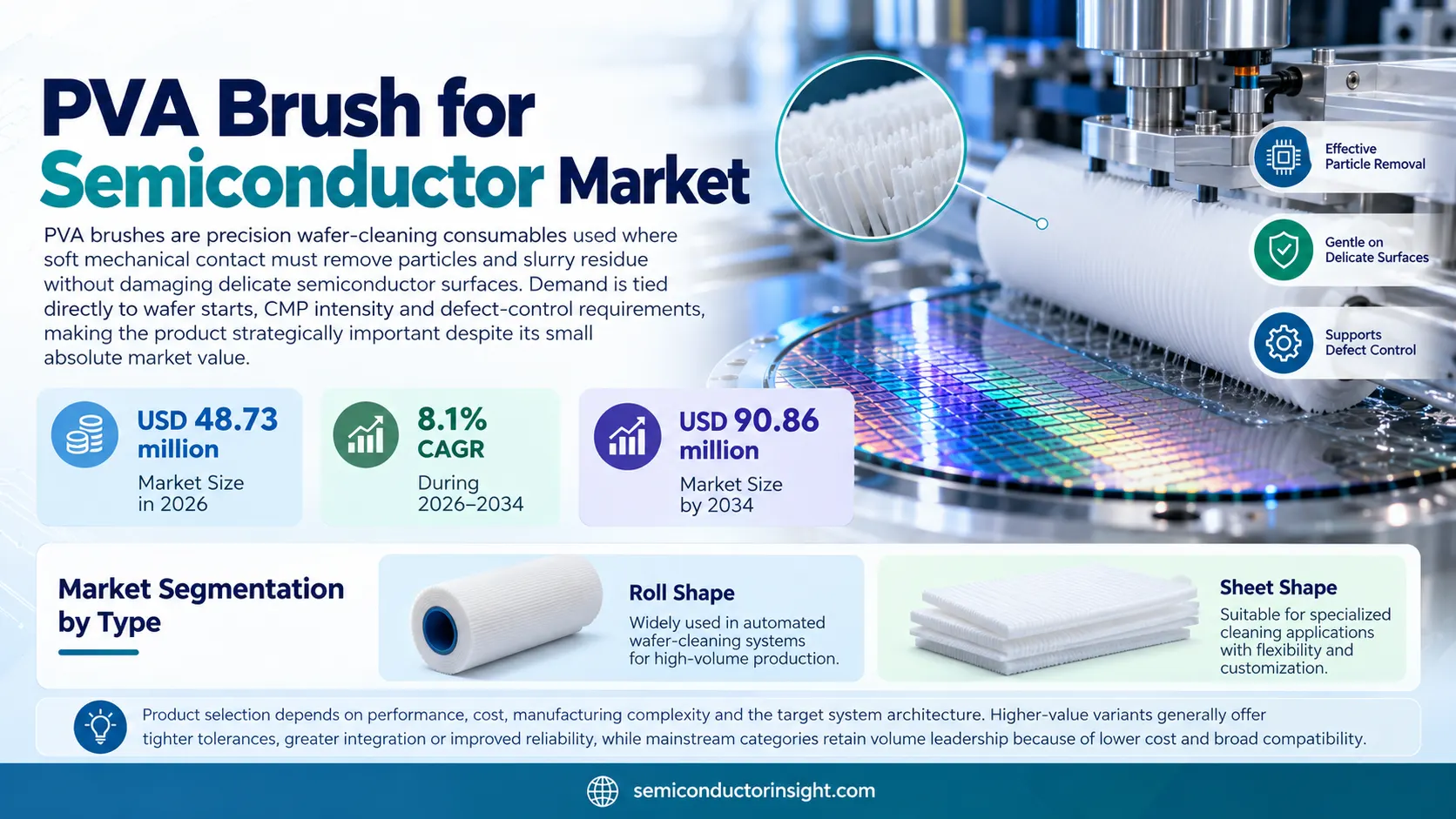
PVA brush for semiconductor market is valued at USD 45.08 million in 2025 and is projected to reach USD 90.86 million by 2034, expanding at a 8.1% CAGR during 2026–2034. The 2026 market level is USD 48.73 million. PVA brushes are precision wafer-cleaning consumables used where soft mechanical contact must remove particles and slurry residue without damaging delicate semiconductor surfaces. Demand is tied directly to wafer starts, CMP intensity and defect-control requirements, making the product strategically important despite its small absolute market value.
Advanced nodes and 3D memory structures reduce the allowable defect budget, raising expectations for brush pore uniformity, dimensional stability, chemical compatibility and low particle shedding. Brush performance is increasingly evaluated together with cleaning chemistry, megasonic settings and equipment recipes rather than as a standalone consumable. Commercial decisions in the PVA Brush for Semiconductor market depend on qualification history, integration effort, operating reliability, lifecycle support and measurable system-level value.
The market is highly qualification-driven because a change in brush geometry or material can alter defectivity and yield. Suppliers therefore compete on consistency, contamination control, application support and production capacity close to major wafer-fabrication clusters. The 300 mm segment is particularly important because leading logic and memory fabs operate at that wafer size.
Segment Analysis: By Type
By type, the market is segmented into Roll Shape, Sheet Shape. Product selection depends on performance, cost, manufacturing complexity and the target system architecture. Higher-value variants generally offer tighter tolerances, greater integration or improved reliability, while mainstream categories retain volume leadership because of lower cost and broad compatibility. Commercial decisions in the PVA Brush for Semiconductor market depend on qualification history, integration effort, operating reliability, lifecycle support and measurable system-level value.
| Type | Commercial role |
|---|---|
| Roll Shape | Roll Shape addresses a distinct requirement set within the PVA Brush for Semiconductor market, with purchasing decisions shaped by performance, qualification, integration and cost. |
| Sheet Shape | Sheet Shape addresses a distinct requirement set within the PVA Brush for Semiconductor market, with purchasing decisions shaped by performance, qualification, integration and cost. |
Additional Segmentation: By Cleaning Stage
Cleaning Stage segmentation highlights important technical and commercial differences inside the PVA Brush for Semiconductor market. These categories affect pricing, qualification, process requirements and customer fit, making them useful for evaluating where value growth differs from simple unit growth. Commercial decisions in the PVA Brush for Semiconductor market depend on qualification history, integration effort, operating reliability, lifecycle support and measurable system-level value.
| Cleaning Stage | Demand characteristics |
|---|---|
| Post-CMP Cleaning | Removes slurry residue and particles after chemical mechanical planarization. |
| Post-Etch / Residue Cleaning | Targets particles and residues after selected plasma or wet-process steps. |
| General Wafer Cleaning | Supports recurring wafer-surface maintenance across semiconductor processing. |
Segment Analysis: By Application
By application, the market covers 300 mm Wafer, 200 mm Wafer, Others. Demand varies by reliability, performance, budget and product lifecycle. Premium applications usually require stricter qualification and long-term supply support, while higher-volume applications place more emphasis on cost, manufacturing scale and rapid technology migration. Commercial decisions in the PVA Brush for Semiconductor market depend on qualification history, integration effort, operating reliability, lifecycle support and measurable system-level value.
| Application | Demand characteristics |
|---|---|
| 300 mm Wafer | 300 mm Wafer is a material demand segment where reliability, cost and system performance influence purchasing decisions. |
| 200 mm Wafer | 200 mm Wafer is a material demand segment where reliability, cost and system performance influence purchasing decisions. |
| Others | Others is a material demand segment where reliability, cost and system performance influence purchasing decisions. |
Additional Segmentation: By End User
End User segmentation clarifies how system architecture and customer requirements reshape product selection. Growth is strongest where the technology delivers a clear performance, cost, reliability or integration advantage relative to incumbent solutions. Commercial decisions in the PVA Brush for Semiconductor market depend on qualification history, integration effort, operating reliability, lifecycle support and measurable system-level value.
| End User | Commercial role |
|---|---|
| Foundries | High-volume logic and specialty wafer fabrication. |
| Memory Manufacturers | DRAM and NAND fabs with intensive CMP and cleaning cycles. |
| IDMs | Integrated logic, analog, power and sensor manufacturing. |
| Equipment OEMs | Cleaning-tool suppliers integrating PVA brush modules into wafer-cleaning systems. |
Regional Analysis
Asia Pacific leads demand because Taiwan, South Korea, China and Japan host the largest concentration of 300 mm fabs, memory capacity and post-CMP cleaning tools. The source indicates 300 mm wafers accounted for 68% of brush sales in 2024. Commercial decisions in the PVA Brush for Semiconductor market depend on qualification history, integration effort, operating reliability, lifecycle support and measurable system-level value.
Why does regional demand differ across the PVA Brush for Semiconductor market?
Regional demand closely follows advanced semiconductor wafer capacity. Asia Pacific dominates volume, North America is important in leading-edge logic and memory, Europe supports automotive and specialty fabs, while other regions remain smaller and more dependent on imported consumables. Commercial decisions in the PVA Brush for Semiconductor market depend on qualification history, integration effort, operating reliability, lifecycle support and measurable system-level value.
How does Asia Pacific participate in the PVA Brush for Semiconductor market?
Asia Pacific demand is anchored by manufacturing scale, electronics production and growing investment in advanced infrastructure. China, Japan, South Korea, Taiwan and India contribute different mixes of production, end-market demand and technical capability, making the region central to both volume growth and supply-chain development. Commercial decisions in the PVA Brush for Semiconductor market depend on qualification history, integration effort, operating reliability, lifecycle support and measurable system-level value.
How does North America participate in the PVA Brush for Semiconductor market?
North America remains a high-value market with strong technology development, enterprise spending and specialized industrial demand. The United States is the principal contributor, supported by leading technology companies, research institutions and high-value end markets that adopt premium solutions early. Commercial decisions in the PVA Brush for Semiconductor market depend on qualification history, integration effort, operating reliability, lifecycle support and measurable system-level value.
How does Europe participate in the PVA Brush for Semiconductor market?
Europe combines advanced manufacturing, healthcare, aerospace, automotive and research demand. Germany, France, the United Kingdom, Italy and other markets emphasize reliability, energy efficiency and regulatory compliance, supporting demand for technically differentiated products with strong lifecycle support. Commercial decisions in the PVA Brush for Semiconductor market depend on qualification history, integration effort, operating reliability, lifecycle support and measurable system-level value.
How does South America participate in the PVA Brush for Semiconductor market?
South America is a smaller but developing market led by Brazil and selected industrial economies. Demand is concentrated in infrastructure, healthcare, electronics, research and industrial modernization, with import dependence making distributor support, service coverage and pricing important commercial factors. Commercial decisions in the PVA Brush for Semiconductor market depend on qualification history, integration effort, operating reliability, lifecycle support and measurable system-level value.
How does Middle East & Africa participate in the PVA Brush for Semiconductor market?
Middle East & Africa remains an emerging market where demand is concentrated in infrastructure, healthcare, energy, defense and research projects. Gulf countries account for much of the premium investment, while wider adoption depends on local technical capability, procurement cycles and access to qualified suppliers. Commercial decisions in the PVA Brush for Semiconductor market depend on qualification history, integration effort, operating reliability, lifecycle support and measurable system-level value.
Competitive Landscape
The competitive landscape includes ITW Rippey, Entegris, Aion, BrushTek, 3M, Techno Medica, MicroCare and PVA TePla. Market position is shaped by technical performance, qualification depth, customer support, manufacturing scale and the ability to support product transitions without disrupting customer operations. Commercial decisions in the PVA Brush for Semiconductor market depend on qualification history, integration effort, operating reliability, lifecycle support and measurable system-level value.
Competition is increasingly centered on lower-particle-shedding PVA, controlled pore structure and predictive brush-life management. Larger suppliers benefit from global engineering resources and purchasing scale, while specialized vendors can defend attractive niches through process expertise, customization and faster technical support. Commercial decisions in the PVA Brush for Semiconductor market depend on qualification history, integration effort, operating reliability, lifecycle support and measurable system-level value.
| Competitive dimension | What matters |
|---|---|
| Technology | Performance, reliability and roadmap credibility. |
| Qualification | Customer validation, compliance and field history. |
| Supply | Capacity, lead time and regional resilience. |
| Commercial support | Application engineering, service and lifecycle support. |
Production Capacity Analysis
Capacity strategy in the PVA Brush for Semiconductor market is closely linked to demand visibility, qualification cycles and customer concentration. Suppliers add capacity carefully because advanced production often requires specialized equipment, process know-how and extended validation before new lines can serve demanding applications. Commercial decisions in the PVA Brush for Semiconductor market depend on qualification history, integration effort, operating reliability, lifecycle support and measurable system-level value.
Regional capacity decisions increasingly balance cost with resilience. Customers are asking suppliers to diversify critical steps, maintain qualified backup capacity and support shorter lead times. That trend favors manufacturers able to combine scale with consistent process control and regional technical support. Commercial decisions in the PVA Brush for Semiconductor market depend on qualification history, integration effort, operating reliability, lifecycle support and measurable system-level value.
Market Dynamics
The PVA Brush for Semiconductor market is shaped by simultaneous changes in end-market demand, product architecture, manufacturing economics and qualification requirements. Technology improvements create new use cases, but commercialization depends on whether performance gains translate into measurable system value. Commercial decisions in the PVA Brush for Semiconductor market depend on qualification history, integration effort, operating reliability, lifecycle support and measurable system-level value.
Supply-chain conditions also influence purchasing behavior. Customers increasingly evaluate continuity, regional sourcing and lifecycle support alongside unit price. This shifts competition toward suppliers that can deliver stable quality and technical service through multiple product generations. Commercial decisions in the PVA Brush for Semiconductor market depend on qualification history, integration effort, operating reliability, lifecycle support and measurable system-level value.
Market Drivers
Growth is driven by rising wafer starts, greater CMP step counts, tighter defect budgets and expansion of advanced logic, HBM and 3D NAND. More frequent cleaning and stricter contamination control increase both brush consumption and the value of higher-performance consumables. Commercial decisions in the PVA Brush for Semiconductor market depend on qualification history, integration effort, operating reliability, lifecycle support and measurable system-level value.
| Driver | CAGR impact |
|---|---|
| Technology upgrade cycle | +1.8 percentage points |
| End-market expansion | +1.3 percentage points |
| Higher content per system | +0.9 percentage points |
Market Restraints
Constraints include demanding dimensional tolerances, qualification costs, consumable price pressure and competition from alternative non-contact cleaning approaches. Small process deviations can affect wafer yield, so manufacturers must maintain very tight production consistency and contamination control. Commercial decisions in the PVA Brush for Semiconductor market depend on qualification history, integration effort, operating reliability, lifecycle support and measurable system-level value.
| Restraint | CAGR impact |
|---|---|
| Qualification and replacement cost | -0.8 percentage points |
| Price pressure | -0.6 percentage points |
| Supply or integration complexity | -0.5 percentage points |
Market Opportunities
Opportunities include 300 mm advanced-node fabs, new HBM and 3D NAND capacity, smart brush-life monitoring and brush formulations optimized for new slurry chemistries. Local supply near major semiconductor clusters can also reduce inventory risk and improve technical response times. Commercial decisions in the PVA Brush for Semiconductor market depend on qualification history, integration effort, operating reliability, lifecycle support and measurable system-level value.
| Opportunity | Commercial significance |
|---|---|
| lower-particle-shedding PVA, controlled pore structure and predictive brush-life management | Supports premium product mix and new design wins. |
| Regional capacity | Improves lead times and customer resilience. |
| Application engineering | Raises switching costs and deepens customer relationships. |
Supply Chain Analysis
The PVA Brush for Semiconductor supply chain spans upstream materials and components, specialized manufacturing, qualification and integration, distribution or direct sales, and end-use deployment. Value is not distributed evenly: the highest margins generally accrue where process know-how, IP, qualification or application engineering create defensible differentiation. Commercial decisions in the PVA Brush for Semiconductor market depend on qualification history, integration effort, operating reliability, lifecycle support and measurable system-level value.
| Stage | Role |
|---|---|
| Upstream inputs | Materials, components, software or specialized process equipment. |
| Manufacturing | Core fabrication, assembly and process control. |
| Qualification & integration | Validation, reliability testing and customer-specific adaptation. |
| End-market deployment | System integration, service and lifecycle support. |
Supply continuity has become strategically important because qualified alternatives may require lengthy validation. Buyers therefore monitor second-source readiness, geographic concentration and supplier financial stability, especially where a single component can delay a high-value system. Commercial decisions in the PVA Brush for Semiconductor market depend on qualification history, integration effort, operating reliability, lifecycle support and measurable system-level value.
Recent Developments in the PVA Brush for Semiconductor Market
Report Scope & Segmentation
This analysis covers the PVA Brush for Semiconductor market from a 2025 base year through the 2026–2034 forecast period. It evaluates demand by product type, application and two additional segmentation axes, with regional coverage spanning Asia Pacific, North America, Europe, South America, and the Middle East & Africa. Commercial decisions in the PVA Brush for Semiconductor market depend on qualification history, integration effort, operating reliability, lifecycle support and measurable system-level value.
| Scope item | Coverage |
|---|---|
| Base year | 2025 |
| Estimated year | 2026 |
| Forecast period | 2026–2034 |
| By Type | Roll Shape, Sheet Shape |
| By Application | 300 mm Wafer, 200 mm Wafer, Others |
| By Cleaning Stage | Post-CMP Cleaning, Post-Etch / Residue Cleaning, General Wafer Cleaning |
| By End User | Foundries, Memory Manufacturers, IDMs, Equipment OEMs |
| Key participants | ITW Rippey, Entegris, Aion, BrushTek, 3M, Techno Medica, MicroCare and PVA TePla |
Frequently Asked Questions
What is the PVA Brush for Semiconductor market size in 2025?
The market is valued at USD 45.08 million in 2025.
What is the market forecast for 2034?
The market is projected to reach USD 90.86 million by 2034, with a 8.1% CAGR during 2026–2034.
Which region leads the market?
Asia Pacific leads current market value, while Asia Pacific has the strongest growth profile.
Which type is most important?
Roll Shape is a leading category, although mix varies by application and performance requirement.
Which applications matter most?
300 mm Wafer is a major demand segment, alongside 200 mm Wafer, Others.
What technology trend matters most?
lower-particle-shedding PVA, controlled pore structure and predictive brush-life management is a central technology and commercialization trend.
Who are the major suppliers?
Major participants include ITW Rippey, Entegris, Aion, BrushTek, 3M, Techno Medica, MicroCare and PVA TePla.
What drives market growth?
Growth is driven by rising wafer starts, greater CMP step counts, tighter defect budgets and expansion of advanced logic, HBM and 3D NAND. More frequent cleaning and stricter contamination control increase both brush con
What limits growth?
Constraints include demanding dimensional tolerances, qualification costs, consumable price pressure and competition from alternative non-contact cleaning approaches. Small process deviations can affect wafer yield, so m
What will shape the market through 2034?
Technology roadmaps, qualification, supply continuity and lower-particle-shedding PVA, controlled pore structure and predictive brush-life management will shape competitive outcomes.
Research Sources & Evidence Base
View selected external research sources
- Entegris — Semiconductor Materials & Contamination Control: Current semiconductor contamination-control context. Open source
- Applied Materials — CMP Technology: Current CMP process and wafer-planarization context. Open source
- Lam Research — Wafer Cleaning: Current semiconductor wafer-cleaning equipment context. Open source
Get Sample Report PDF for Exclusive Insights
Report Sample Includes
- Table of Contents
- List of Tables & Figures
- Charts, Research Methodology, and more...
 Download Sample Report PDF