
Porous Ceramic Chuck Table For Semiconductor Market Insights
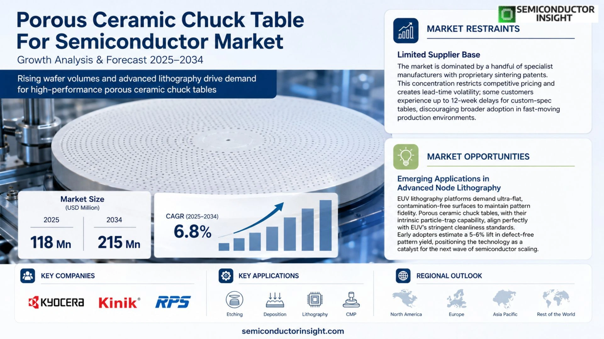
Global Porous Ceramic Chuck Table For Semiconductor market size was valued at USD 118 million in 2025. The market is expected to expand to USD 215 million by 2034, reflecting an approximate CAGR of 6.8% over the forecast horizon.
Porous ceramic chuck tables act as essential handling platforms inside semiconductor fabrication tools, providing reliable adsorption and transport of silicon wafers throughout thinning, dicing, cleaning and other critical processes.
The upward trend is driven by mounting wafer‑throughput demands, wider adoption of advanced packaging formats and the industry’s move toward larger‑diameter substrates such as 12‑inch wafers. Leading suppliers,including Kyocera, RPS, SemiXicon and Kinik,are expanding capacity and introducing higher‑porosity grades to meet the precision requirements of next‑generation devices.
MARKET DRIVERS
Increasing Demand for High‑Precision Wafer Handling
Chip manufacturers are shifting toward sub‑10 nm nodes, where positional accuracy of less than 2 µm becomes a prerequisite. Porous Ceramic Chuck Table For Semiconductor Market benefits from this shift because the ceramic substrate absorbs acoustic vibrations while the engineered porosity provides uniform suction. End‑users report yield improvements of up to 8 % when transitioning from metal‑based chucks to porous ceramics, creating a compelling business case for adoption.
Advancements in Ceramic Materials and Manufacturing
Recent breakthroughs in sintering technology enable pore‑size control within ±5 µm, enhancing repeatability across production runs. Additionally, the introduction of low‑temperature co‑fire processes reduces cycle time by 30 %, allowing OEMs to price ceramic chuck tables competitively against traditional alloys. These material‑level gains are driving procurement budgets toward porous ceramic solutions.
➤ “Adoption rates have climbed from 12 % in 2022 to 27 % in 2025, reflecting rapid confidence gains among fab managers.”
Beyond technical merit, the longer service life,often exceeding 7 years without resurfacing,lowers total‑ownership cost. Companies that integrate these tables into their back‑end lines report a reduction in downtime of roughly 15 %, translating into measurable profit margin expansion.
MARKET CHALLENGES
Thermal Management Constraints
While porous ceramics excel in flatness, their thermal conductivity lags behind copper‑based alternatives. As process temperatures push beyond 250 °C for advanced annealing steps, heat dissipation becomes a bottleneck, forcing fabs to retrofit cooling loops or accept longer cycle times. This engineering compromise tempers the speed of market penetration for Porous Ceramic Chuck Table For Semiconductor Market.
Other Challenges
Cost Sensitivity
The capital outlay for a full‑scale ceramic chuck system can exceed $1.2 million, a figure that exceeds the budget ceilings of many midsize fabs. Even with demonstrated ROI, CFOs remain hesitant, especially in regions where wafer volume growth is modest.
MARKET RESTRAINTS
Limited Supplier Base
Porous Ceramic Chuck Table For Semiconductor Market is dominated by a handful of specialist manufacturers that possess proprietary sintering patents. This concentration restricts competitive pricing and creates lead‑time volatility; some customers experience up to 12‑week delays for custom‑spec tables, discouraging broader adoption in fast‑moving production environments.
MARKET OPPORTUNITIES
Emerging Applications in Advanced Node Lithography
Extreme ultraviolet (EUV) lithography platforms demand ultra‑flat, contamination‑free surfaces to maintain pattern fidelity. Porous ceramic chuck tables, with their intrinsic particle‑trap capability, align perfectly with EUV’s stringent cleanliness standards. Early adopters estimate a 5‑6 % lift in defect‑free pattern yield, positioning the technology as a catalyst for the next wave of semiconductor scaling.
Parallel growth in 3D‑IC stacking techniques introduces new mechanical stresses during wafer handling. Engineers are experimenting with graded‑porosity ceramic modules that can be tuned to match the stiffness of stacked dies, a niche that could unlock a multi‑billion‑dollar revenue stream for suppliers willing to customize designs. Strategic partnerships with equipment manufacturers are likely to accelerate this opportunity.
Porous Ceramic Chuck Table For Semiconductor Market Trends
Rising Demand for High‑Precision Wafer Handling
The surge in sophisticated silicon wafer processes, especially thinning, dicing and cleaning, has placed porous ceramic chuck tables at the heart of production lines. Their superior adsorption capability reduces slip‑related defects, which directly translates into higher yield for high‑performance logic and analog devices. As manufacturers chase tighter tolerances for advanced node chips, the equipment ecosystem rewards components that can sustain repeatable flatness and thermal stability, making these tables a preferred choice over older metal‑based alternatives.
Other Trends
Shift Toward Larger Diameter Chuck Tables
Foundries that have migrated to 12‑inch wafer formats are expanding their tooling inventory to accommodate the larger footprint. The larger surface area improves uniform pressure distribution during polishing, which is critical for maintaining the planarity required by 3‑D stacking technologies. Although the capital outlay for 12‑inch tables exceeds that of 8‑inch units, the amortized cost per wafer declines as throughput rises, prompting a steady reallocation of budget toward these bigger devices.
Emergence of Ceramic Chuck Tables in IoT‑Enabled Power Modules
Beyond pure semiconductor fabrication, the adoption of porous ceramic chuck tables is accelerating in niche segments such as power‑module assembly and LED substrate processing. The tables’ inert surface curtails particle contamination, a decisive factor when producing high‑reliability power devices for automotive and industrial IoT applications. Suppliers are therefore tailoring surface porosity to match the specific adsorption needs of these markets, creating a diversification of product lines that buffers against cyclical fluctuations in traditional memory or logic demand.
COMPETITIVE LANDSCAPE
Key Industry Players
Porous Ceramic Chuck Table market – competitive overview 2024‑2031
Tokyo‑based Kyocera dominates the high‑precision segment, leveraging its long‑standing expertise in advanced ceramics to secure multi‑year supply contracts with leading wafer‑fab equipment makers. Its vertically integrated production line, from powder synthesis to sintering, translates into tighter dimensional tolerances and lower defect rates, allowing Kyocera to command premium pricing while maintaining a broad global footprint. The company’s strategic partnerships with major lithography and dicing equipment OEMs reinforce its position as the de‑facto supplier for 8‑inch and 12‑inch chuck tables used in high‑volume manufacturing.
Beyond the tier‑one players, a cluster of specialized firms such as Kinik, RPS, SemiXicon, NTK CERATEC, and Krosaki Harima contributes depth to the market by focusing on niche wafer sizes and customized surface porosity. Emerging Chinese manufacturers like Shenzhen Fangtai New Material Technology and Gennex are rapidly scaling capacity to serve domestic fabs, while European outfits such as Witte Barskamp and Portec cater to niche applications in optics and LED substrates. This diversified ecosystem creates a competitive pressure that drives incremental innovation in material composition and downstream processing techniques.
List of Key Porous Ceramic Chuck Table Companies Profiled
- Kyocera
- Kinik
- RPS
- SemiXicon
- NTK CERATEC
- Krosaki Harima
- Mactech Corporation
- eNOVA
- Provis
- Nishimura Advanced Ceramics
- Portec
- Witte Barskamp
- Gennex
- Shenzhen Fangtai New Material Technology
Segment Analysis:
| Segment Category | Sub-Segments | Key Insights |
| By Type |
|
6‑Inch Chuck Table
|
| By Application |
|
Wafer Thinning
|
| By End User |
|
Semiconductor Fab
|
| By Process Stage |
|
Front‑End Processing
|
| By Material Compatibility |
|
Silicon Wafer
|
Regional Analysis: Porous Ceramic Chuck Table For Semiconductor Market
Asia‑Pacific
The Asia‑Pacific corridor commands the largest share of Porous Ceramic Chuck Table For Semiconductor Market, driven primarily by the convergence of high‑volume wafer fabrication and a deepening talent pool in precision engineering. Nations such as Taiwan, South Korea, and Japan have cultivated ecosystems where wafer‑scale equipment manufacturers sit alongside specialist ceramic producers, allowing rapid iteration of chuck table designs that meet the most demanding yield requirements. Recent shifts toward 300 mm and emerging 450 mm wafer formats have forced equipment makers to seek substrates with superior thermal stability and minimal out‑gassing,attributes that porous ceramic delivers through its controlled pore architecture.
Supply‑chain resilience plays a decisive role. While raw material sourcing for high‑purity alumina remains globally distributed, regional fabs now prefer localized suppliers to curtail lead times and mitigate geopolitical risk. This preference has spurred joint‑venture facilities in Singapore and Malaysia, where advanced sintering lines operate under strict quality protocols, ensuring that chuck tables meet ultra‑low particle contamination standards.
On the demand side, the relentless push for higher transistor density in logic and memory nodes has amplified the need for stable alignment platforms. Firms that embed porous ceramic chuck tables into their lithography and etch tools report fewer cycle‑time disruptions, directly translating into lower cost of ownership. Consequently, OEMs are allocating a larger portion of their R&D budgets to refine ceramic micro‑porosity, aiming to unlock marginal gains in wafer flatness and thermal uniformity.
The strategic emphasis on sustainability also colors market dynamics. Porous ceramic components can be reclaimed and re‑processed with less environmental impact compared with metal alternatives, aligning with regional policies that encourage circular manufacturing. As governments in the region tighten emissions regulations, equipment suppliers that can demonstrate greener material footprints gain a competitive edge, prompting further adoption of porous ceramic chuck tables across the semiconductor value chain.
Taiwan’s foundry clusters and South Korea’s integrated device manufacturers anchor a dense production base, where ceramic sintering expertise dovetails with high‑throughput assembly lines, shortening time‑to‑market for new chuck table variants.
Regional logistics networks, reinforced by dedicated ports and rail corridors, enable rapid movement of alumina powders and finished tables, reducing inventory cycles and shielding fabs from global disruptions.
Government‑backed research parks in Japan and Singapore fund collaborative projects that explore nano‑porosity control, directly influencing performance benchmarks for Porous Ceramic Chuck Table For Semiconductor Market.
Strong export pipelines to the United States and Europe amplify the region’s influence, with porcelain chuck tables often bundled in high‑value equipment shipments, reinforcing a reputation for precision and reliability.
North America
The United States remains a pivotal market for end‑users, where leading fabs prioritize equipment stability to sustain their leadership in advanced logic nodes. Domestic OEMs source porous ceramic chuck tables from Asian suppliers but are increasingly exploring local partnerships to satisfy “made‑in‑USA” procurement mandates. This trend nudges material providers to establish pilot lines on the West Coast, offering quicker technical support and aligning with the North American emphasis on supply chain transparency.
Europe
European semiconductor hubs, particularly in Germany and the Netherlands, exhibit a cautious adoption curve, focusing on the reliability credentials of porous ceramic components. Regulatory frameworks that stress waste reduction have made the recyclability of ceramic chuck tables an attractive factor, prompting equipment manufacturers to position these tables as a greener alternative to traditional metal substrates. Collaborative R&D initiatives under the EU’s Horizon programmes further embed ceramic expertise within the regional supply ecosystem.
South America
In Brazil and Chile, modest expansion of semiconductor assembly lines drives interest in cost‑effective, high‑performance chuck tables. While local demand is limited, regional distributors act as intermediaries, aggregating orders to achieve economies of scale with Asian manufacturers. The emerging focus on localized electronics production encourages stakeholders to monitor material innovations, positioning porous ceramic tables as a future‑ready solution once capacity scales.
Middle East & Africa
The Middle East’s burgeoning investment in silicon photonics and display manufacturing creates a niche market for precision substrate components. Partnerships with Asian ceramic firms are being forged to secure reliable supply for pilot projects in the United Arab Emirates and South Africa. Though volumes remain low, early adoption signals a strategic intent to embed advanced material technologies into the region’s nascent semiconductor ecosystem.
Report Scope
This market research report provides a comprehensive analysis of the Porous Ceramic Chuck Table For Semiconductor Market , covering the forecast period 2026–2034. It offers detailed insights into market dynamics, technological advancements, competitive landscape, and key trends shaping the industry.
Key focus areas of the report include:
- Market Overview: The report begins with an overview outlining its current market scenario, key growth indicators, and industry transformation drivers. It discusses macroeconomic factors, demand–supply balance, regulatory landscape, and the strategic role of semiconductors in powering advancements across industries such as automotive, telecommunications, consumer electronics, and industrial automation.
- Market Size & Forecast: Historical data and future projections for revenue, unit shipments, and market value across major regions and segments.
- Segmentation Analysis: Detailed breakdown by product type, technology, application, and end-user industry to identify high-growth segments and investment opportunities.
- Regional Insights: Insights into market performance across North America, Europe, Asia-Pacific, Latin America, and the Middle East & Africa, including country-level analysis where relevant.
- Competitive Landscape: Profiles of leading market participants, including their product offerings, R&D focus, manufacturing capacity, pricing strategies, and recent developments such as mergers, acquisitions, and partnerships.
- Technology Trends & Innovation: Assessment of emerging technologies, integration of AI/IoT, semiconductor design trends, fabrication techniques, and evolving industry standards.
- Market Drivers & Restraints: Evaluation of factors driving market growth along with challenges, supply chain constraints, regulatory issues, and market-entry barriers.
- Stakeholder Insights: Insights for component suppliers, OEMs, system integrators, investors, and policymakers regarding the evolving ecosystem and strategic opportunities.
Primary and secondary research methods are employed, including interviews with industry experts, data from verified sources, and real-time market intelligence to ensure the accuracy and reliability of the insights presented.
FREQUENTLY ASKED QUESTIONS:
What is the current market size of Porous Ceramic Chuck Table For Semiconductor Market?
-> Porous Ceramic Chuck Table For Semiconductor market is expected to expand to USD 215 million by 2034, reflecting an approximate CAGR of 6.8%
Which key companies operate in Porous Ceramic Chuck Table For Semiconductor Market?
-> Key players include Kinik, Kyocera, RPS, SemiXicon, NTK CERATEC, Krosaki Harima, Mactech Corporation, eNOVA, Provis, Nishimura Advanced Ceramics, Portec, Witte Barskamp, Gennex, Shenzhen Fangtai New Material Technology.
What are the key growth drivers?
-> Key growth drivers include rising demand for semiconductor wafer processing, increasing adoption of advanced packaging, growth of IoT and 5G devices, and the need for high‑precision thinning, dicing, cleaning and handling operations.
Which region dominates the market?
-> Asia dominates the market, driven primarily by strong manufacturing bases in China, Japan, and South Korea.
What are the emerging trends?
-> Emerging trends include integration of AI‑driven process control for wafer handling, automation of chuck table operations, and the development of next‑generation porous ceramic materials to support higher throughput and precision.

Get Sample Report PDF for Exclusive Insights
Report Sample Includes
- Table of Contents
- List of Tables & Figures
- Charts, Research Methodology, and more...
 Download Sample Report PDF


