
Nanoimprint Lithography (NIL) for Semiconductors Market Insights
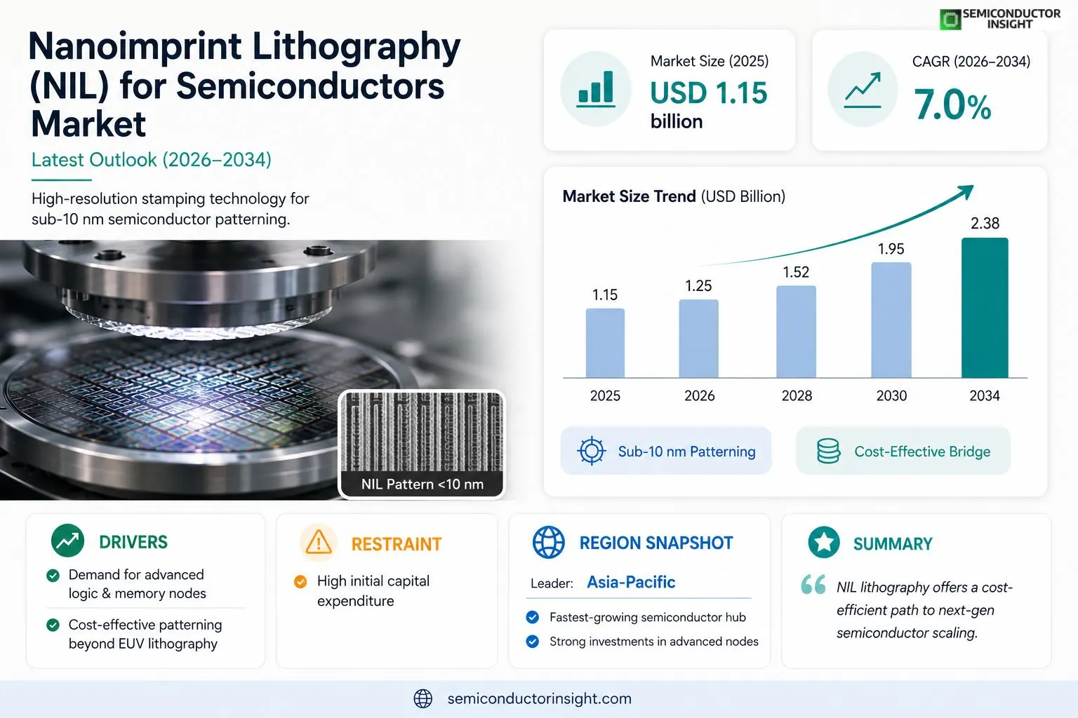
Global NIL for semiconductors market size was valued at USD 1.15 billion in 2025. The market is projected to grow from USD 1.25 billion in 2026 to USD 2.38 billion by 2034, exhibiting a CAGR of 7.0% during the forecast period.
Nanoimprint lithography (NIL) is a high‑resolution patterning technique that transfers nanoscale features onto semiconductor wafers through a physical stamping process, enabling sub‑10 nm critical dimensions with reduced cycle time and lower cost compared with traditional photolithography.The market is experiencing rapid growth due to several factors, including rising demand for advanced nodes in logic and memory chips, increased investment in heterogeneous integration, and the need for cost‑effective patterning solutions beyond extreme ultraviolet (EUV) lithography. Furthermore, recent collaborationssuch as the partnership announced in March 2024 between a leading equipment supplier and a major foundry to co‑develop high‑throughput NIL toolsare expected to accelerate adoption across the semiconductor supply chain.
MARKET DRIVERS
Cost Efficiency and Throughput Gains
Nanoimprint Lithography (NIL) for Semiconductors Market is gaining traction because it can lower per‑wafer cost by up to 30 % compared with traditional EUV lithography, while maintaining comparable throughput. Manufacturers report that the reduced cycle time translates into higher line utilization and faster time‑to‑market for new node products.
Pattern Fidelity for Advanced Nodes
Recent process refinements allow NIL to achieve sub‑10 nm pattern fidelity, supporting the roadmap for 3‑nm and beyond. This precision enables designers to pack more transistors per die, directly boosting performance per wattan essential metric for data‑center and AI accelerators.
➤ NIL’s ability to replicate nanoscale templates with minimal overlay error is a decisive advantage for heterogeneous integration.
Overall, the alignment of cost savings, high resolution, and compatibility with existing silicon‑on‑insulator platforms positions NIL as a compelling alternative for semiconductor fabs seeking sustainable growth.
MARKET CHALLENGES
Process Integration Complexity
Integrating NIL into mainstream semiconductor lines requires redesign of resist chemistry, temperature control, and defect‑inspection workflows. Many fabs face a steep learning curve, and the need for specialized metrology tools can extend ramp‑up periods.
Other Challenges
Equipment Reliability
Long‑term reliability of imprint tools under high‑volume production remains uncertain. Operators report accelerated wear on stamp surfaces, prompting additional maintenance cycles that can offset some of the cost advantages.
MARKET RESTRAINTS
High Initial Capital Expenditure
The upfront investment for NIL equipment, including imprint scanners and template fabrication stations, often exceeds $150 million for a full wafer‑scale line. This barrier deters smaller foundries and limits rapid adoption across the broader semiconductor ecosystem.
MARKET OPPORTUNITIES
Emerging Applications in Photonic ICs
Beyond logic chips, NIL is uniquely suited for creating high‑resolution photonic structures such as waveguides and metasurfaces. The growing demand for optical interconnects and LiDAR modules opens a new revenue stream, allowing NIL technology to diversify beyond traditional transistor patterning.
Nanoimprint Lithography (NIL) for Semiconductors Market Trends
Accelerated Adoption Fueled by Advanced Node Requirements
Nanoimprint Lithography (NIL) for Semiconductors Market is witnessing a pronounced shift as chip designers target sub‑10 nm critical dimensions for logic and memory products. The physical stamping method delivers pattern fidelity that rivals extreme ultraviolet (EUV) lithography while cutting cycle time and equipment cost. Semiconductor manufacturers are increasingly prioritizing NIL to meet the throughput demands of heterogeneous integration, where multiple functionalities are embedded in a single wafer. This pressure is amplified by the need for cost‑effective patterning solutions that sustain Moore’s Law without inflating fab expenditures. Consequently, NIL is emerging as a pragmatic complement to existing photolithography stacks, enabling faster prototype cycles and more aggressive node scaling across the supply chain.
Other Trends
Cost Competitiveness and Cycle Time Reduction
The imprint approach leverages a hard‑mask stamp to directly transfer nanoscale features, eliminating multiple exposure steps required by conventional optics. This simplification translates into lower material consumption and reduced energy use per wafer. In practice, fabs report a measurable shrinkage of cycle time by up to 30 % when transitioning from EUV to NIL for specific pattern layers, while maintaining comparable defect densities. The cost advantage is further reinforced by the ability to reuse stamps across large volumes, providing economies of scale that are particularly attractive for high‑volume logic and memory production.
Strategic Partnerships Strengthen Ecosystem
A notable development occurred in March 2024 when a leading equipment supplier announced a joint venture with a major foundry to co‑develop high‑throughput NIL tools. The collaboration focuses on integrating advanced metrology, real‑time defect detection, and automated stamp replacement within a single production line. Early pilot runs have demonstrated throughput levels compatible with mainstream wafer fab schedules, encouraging broader adoption among tier‑1 manufacturers. This partnership exemplifies the broader trend of ecosystem consolidation, where equipment makers, material providers, and chipmakers align roadmaps to accelerate technology transfer and mitigate risk, thereby reinforcing the market’s growth trajectory.
COMPETITIVE LANDSCAPEKey Industry Players
Emerging NIL Technology Shaping Semiconductor Fabrication
NIL Market is currently anchored by a small cohort of equipment manufacturers that dominate high‑volume wafer‑scale production. EV Group (EVG) leads the segment with its advanced imprint tools that support sub‑10 nm critical dimensions, benefiting from long‑standing collaborations with leading foundries such as TSMC and Samsung. SUSS MicroTec complements EVG by offering complementary process modules, including resist coating and pattern transfer, which enable end‑to‑end NIL workflows for logic and memory nodes. Recent joint ventures between these leaders and major fab operators have accelerated adoption, driving the market toward a projected CAGR of 7 % through 2034. The competitive dynamics are further shaped by strategic patents covering mold fabrication, imprint pressure control, and defect mitigation, which create high entry barriers for new entrants.Beyond the dominant tier, a number of niche players contribute specialized capabilities that broaden NIL’s application spectrum. Nanonex (Canon) supplies mid‑range imprint systems optimized for MEMS and photonic devices, while Picosun focuses on low‑cost, high‑throughput tools for advanced packaging. Molecular Imprints and ION X (formerly RIST) differentiate through proprietary imprint resists and nano‑template technologies. Additional innovators such as NanoInk (now part of ASML), Tokyo Electron, and Advanced Lithography Solutions provide complementary services ranging from mold replication to metrology, reinforcing a fragmented but highly collaborative ecosystem that supports both emerging and legacy semiconductor processes.
List of Key Nanoimprint Lithography Companies Profiled
- EV Group (EVG)
- SUSS MicroTec
- Nanonex (Canon)
- Picosun
- Molecular Imprints
- ION X (formerly RIST)
- NanoInk (ASML)
- Tokyo Electron
- Advanced Lithography Solutions
- IBM Research
- Samsung Advanced Process
- TSMC NIL Exploration Team
- Intel Nanoimprint Program
- Hitachi High‑Tech
- GlobalFoundries NIL Initiative
Segment Analysis:
| Segment Category | Sub-Segments | Key Insights |
| By Type |
|
UV-NIL
|
| By Application |
|
Logic Devices
|
| By End User |
|
Foundries
|
| By Integration Approach |
|
Heterogeneous Integration
|
| By Cost Sensitivity |
|
High‑volume low‑cost production
|
Regional Analysis: North America
United States
NIL is gaining traction in the display industry for fabricating advanced display structures, including transparent and flexible displays. Its ability to create intricate patterns with high resolution is crucial for enhancing display quality and efficiency.
The rise of flexible electronics is creating new opportunities for NIL. This technology allows for the fabrication of conductive and dielectric layers on flexible substrates, paving the way for wearable devices and foldable displays.
NIL is being explored for advanced semiconductor packaging to enable higher integration density and improved performance. Its precise patterning capabilities are well-suited for creating complex interconnects and micro-features in packaging.
NIL is emerging as a viable technique for fabricating photonic devices, including waveguides and optical resonators, which are essential components in optical communication systems. Its ability to transfer nanoscale patterns with high fidelity is particularly valuable in this domain.
Europe
Europe represents a significant and steadily growing market for NIL in the semiconductor sector. Driven by strong research collaborations and a focus on sustainable technologies, European countries like Germany, the Netherlands, and the UK are investing heavily in NIL development. The region benefits from a strong foundation in micro and nanoelectronics, coupled with government initiatives supporting advanced manufacturing. Applications in areas like advanced packaging for automotive electronics and energy-efficient devices are key drivers. While the market is more fragmented compared to the US, collective investments and collaborative projects are fostering innovation and expanding the adoption of NIL. The emphasis on circular economy principles also aligns with NIL’s potential for low-waste manufacturing processes.
Asia-Pacific
Asia-Pacific, particularly countries like Japan, South Korea, and Taiwan, is witnessing rapid growth in the NIL for Semiconductors Market. This expansion is fueled by a highly competitive semiconductor industry and substantial investments in advanced manufacturing capabilities. The region’s strong focus on high-performance computing and 5G infrastructure drives demand for NIL solutions in advanced packaging and interconnect technologies. Japan and South Korea are at the forefront of NIL technology development, with numerous companies actively engaged in research, development, and commercialization. The burgeoning flexible electronics market in the region further contributes to the growth of NIL applications. Government support and private sector investments are synergistically driving the adoption of NIL across various semiconductor segments.
South America
The South American market for NIL in the semiconductor industry is currently in its nascent stages but presents promising growth potential. Increasing investments in electronics manufacturing and a growing demand for sophisticated electronic devices are expected to drive the adoption of NIL technologies. Countries like Brazil and Argentina are witnessing growing interest in NIL for applications in flexible electronics, sensors, and advanced packaging. However, the market faces challenges related to infrastructure development and limited availability of advanced manufacturing expertise. Government initiatives aimed at promoting technological innovation and attracting foreign investment could significantly accelerate the growth of NIL in the region.
Middle East & Africa
The Middle East & Africa region represents a relatively small but emerging market for NIL in the semiconductor sector. The expansion of electronics manufacturing in countries like the UAE and Saudi Arabia, coupled with increasing investments in infrastructure and technology, is expected to drive gradual adoption. While significant investment in NIL is currently limited, the region’s focus on smart city initiatives and advanced industrialization could create future opportunities. The growth of the consumer electronics market and the increasing demand for sophisticated electronic devices are also expected to contribute to the market’s expansion. Government policies promoting technological development and attracting foreign investment will be crucial for unlocking the full potential of NIL in this region.
Report Scope
This market research report provides a comprehensive analysis of the Nanoimprint Lithography (NIL) for Semiconductors Market , covering the forecast period 2026–2034. It offers detailed insights into market dynamics, technological advancements, competitive landscape, and key trends shaping the industry.
Key focus areas of the report include:
- Market Overview: The report begins with an overview outlining its current market scenario, key growth indicators, and industry transformation drivers. It discusses macroeconomic factors, demand–supply balance, regulatory landscape, and the strategic role of semiconductors in powering advancements across industries such as automotive, telecommunications, consumer electronics, and industrial automation.
- Market Size & Forecast: Historical data and future projections for revenue, unit shipments, and market value across major regions and segments.
- Segmentation Analysis: Detailed breakdown by product type, technology, application, and end-user industry to identify high-growth segments and investment opportunities.
- Regional Insights: Insights into market performance across North America, Europe, Asia-Pacific, Latin America, and the Middle East & Africa, including country-level analysis where relevant.
- Competitive Landscape: Profiles of leading market participants, including their product offerings, R&D focus, manufacturing capacity, pricing strategies, and recent developments such as mergers, acquisitions, and partnerships.
- Technology Trends & Innovation: Assessment of emerging technologies, integration of AI/IoT, semiconductor design trends, fabrication techniques, and evolving industry standards.
- Market Drivers & Restraints: Evaluation of factors driving market growth along with challenges, supply chain constraints, regulatory issues, and market-entry barriers.
- Stakeholder Insights: Insights for component suppliers, OEMs, system integrators, investors, and policymakers regarding the evolving ecosystem and strategic opportunities.
Primary and secondary research methods are employed, including interviews with industry experts, data from verified sources, and real-time market intelligence to ensure the accuracy and reliability of the insights presented.
FREQUENTLY ASKED QUESTIONS:
What is the current market size of Nanoimprint Lithography (NIL) for Semiconductors Market?
-> Nanoimprint Lithography (NIL) for Semiconductors Market was valued at USD 1.15 billion in 2025 and is expected to reach USD 2.38 billion by 2034.
Which key companies operate in Nanoimprint Lithography (NIL) for Semiconductors Market?
-> Key players include leading semiconductor equipment manufacturers and major foundries; specific company names are not disclosed in the provided excerpt.
What are the key growth drivers?
-> Key growth drivers include rising demand for advanced nodes in logic and memory chips, increased investment in heterogeneous integration, and the need for cost‑effective patterning solutions beyond EUV lithography.
Which region dominates the market?
-> Regional dominance is not specified in the supplied information.
What are the emerging trends?
-> Emerging trends involve high‑throughput NIL tool development through collaborations between equipment suppliers and major foundries, aiming to accelerate adoption across the semiconductor supply chain.

Get Sample Report PDF for Exclusive Insights
Report Sample Includes
- Table of Contents
- List of Tables & Figures
- Charts, Research Methodology, and more...
 Download Sample Report PDF


