Military Grade 12-inch Silicon Wafer Market Insights
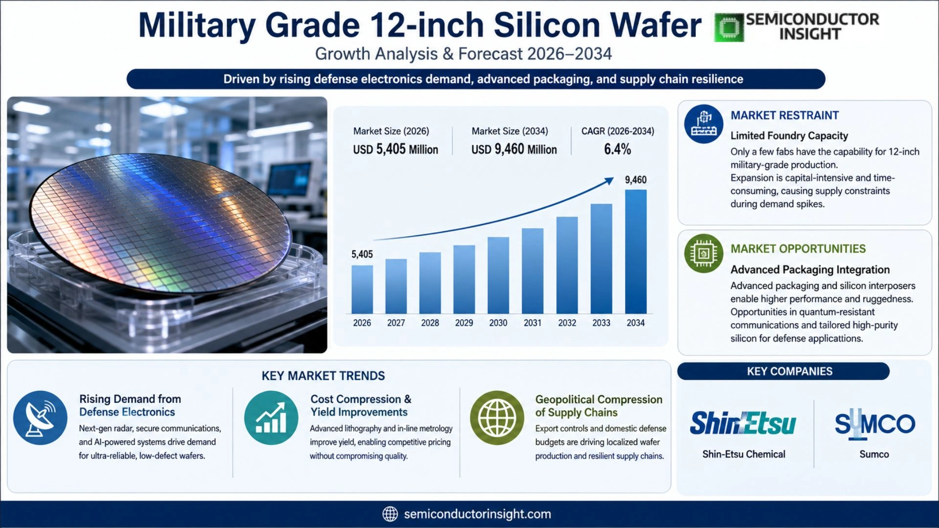
Global Military Grade 12‑inch Silicon Wafer market size was valued at USD 5,070 million in 2024, reached an estimated USD 5,405 million in 2026 and is projected to climb to USD 9,460 million by 2034, reflecting an implied compound annual growth rate of roughly 6.4% over the period.
In electronics, a wafer,also called a slice or substrate,is a thin crystalline silicon disc used as the foundational platform for integrated‑circuit fabrication and photovoltaic cell production; a military‑grade wafer meets stringent specifications for radiation hardness, low defect density and dimensional stability required by defense applications.
MARKET DRIVERS
Rising Defense Electronics Complexity
Modern combat platforms increasingly rely on high‑performance radar, phased‑array antennas, and quantum‑grade sensors. These subsystems demand wafers that meet exacting defect‑density thresholds and can operate under extreme temperature swings. Manufacturers that can certify 12‑inch silicon as “military grade” gain a decisive advantage, because a single wafer can host more circuits than smaller formats, reducing line‑time and logistics footprints for defense contractors.
Government Procurement Policies Favor Domestic Sources
Recent amendments to defense acquisition regulations prioritize domestically produced silicon that complies with ITAR and other security frameworks. This policy shift nudges prime contractors toward suppliers that demonstrate clean‑room capability and traceable supply chains. The resulting procurement preference translates into a steady order pipeline, especially for programs that cannot tolerate foreign‑origin components.
➤ “Strategic autonomy in semiconductor supply is no longer a theoretical goal; it is a contractual requirement for many defense contracts.”
Because 12‑inch wafers enable higher transistor density, system designers can consolidate multiple functions onto a single chip, cutting weight and power consumption,critical metrics for airborne and naval assets. This efficiency incentive directly fuels demand for qualified military‑grade silicon, reinforcing the upward trend observed over the past several years.
MARKET CHALLENGES
Stringent Qualification Timelines
Defense programs often enforce accelerated qualification cycles to meet operational deadlines. The rigorous testing regimen for each wafer batch,covering radiation hardness, thermal cycling, and mechanical shock,can clash with short‑lead‑time expectations, creating a bottleneck for suppliers that lack a mature qualification infrastructure.
Other Challenges
Cost Sensitivity
Even though defense budgets are sizable, each dollar spent on silicon must be justified against the mission cost. The premium associated with clean‑room environments, enhanced inspection protocols, and security clearances raises the unit price of military‑grade wafers, prompting procurement officers to scrutinize every purchase.
MARKET RESTRAINTS
Limited Foundry Capacity
Only a handful of fabs worldwide possess the equipment and clean‑room classifications required for 12‑inch military‑grade production. Expansion projects are capital‑intensive and span multiple years, meaning that sudden spikes in demand can outpace the current supply capability. This capacity constraint caps market expansion despite favorable procurement trends.
MARKET OPPORTUNITIES
Advanced Packaging Integration
Emerging packaging technologies such as silicon‑interposers and heterogeneous integration are reshaping the defense semiconductor landscape. By pairing military‑grade 12‑inch wafers with these advanced packages, system architects can achieve unprecedented performance envelopes while preserving ruggedness. Suppliers that develop turnkey solutions integrating wafer fabrication with specialized packaging stand to capture a growing share of defense contracts.
In parallel, the increasing emphasis on quantum‑resistant communication links opens a niche for high‑purity silicon substrates that can sustain low‑noise, high‑frequency operation. Companies that invest in research collaborations with defense labs to tailor crystal orientation and doping profiles may unlock new revenue streams as the government seeks hardened quantum components.
Military Grade 12-inch Silicon Wafer Market Trends
Rising Demand from Defense Electronics
Military Grade 12-inch Silicon Wafer Market is feeling a pronounced pull from next‑generation defense platforms. Modern radar arrays, secure communication links, and high‑energy laser systems all rely on wafers that can guarantee low defect densities under extreme operating conditions. As armed forces transition from legacy analog modules to digitally‑steered phased‑array and AI‑augmented sensor suites, the criteria for wafer qualification tighten, prompting buyers to favor suppliers that can certify batch‑level reliability. This shift not only lifts order volumes but also forces manufacturers to embed more rigorous testing protocols, thereby raising the overall value proposition of each wafer delivered.
Other Trends
Cost Compression and Yield Improvements
Alongside the demand surge, pricing pressure is reshaping the supply side of Military Grade 12-inch Silicon Wafer Market. Customers negotiate tighter unit costs while still insisting on the stringent defect thresholds required for mission‑critical applications. In response, fab operators are investing in advanced lithography alignment and in‑line metrology to boost first‑pass yield. The resulting efficiency gains translate into a narrower price band,typically a few hundred to a few thousand dollars per wafer,without compromising the high‑purity silicon crystal quality that defense contracts demand. This balance of cost and performance is becoming a decisive factor when OEMs select a wafer partner.
Geopolitical Compression of Supply Chains
Strategic considerations are now dictating how Military Grade 12-inch Silicon Wafer Market sources its raw materials and equipment. Export controls and regional trade tensions have encouraged major producers to diversify manufacturing footprints, establishing secondary lines in North America and Europe to mitigate the risk of single‑source disruption. At the same time, domestic defense budgets are earmarking funds for on‑shore wafer capacity, reinforcing a trend toward localized supply chains. The combined effect is a market environment where resilience, rather than sheer scale, determines competitive advantage, prompting firms to reassess inventory strategies and partner ecosystems.
COMPETITIVE LANDSCAPE
Key Industry Players
Military Grade 12‑inch Silicon Wafer – Competitive Overview
Shin‑Etsu Chemical continues to dominate the military‑grade 12‑inch wafer segment, leveraging its extensive crystal‑growth capacity and deep relationships with defense contractors. Its ability to guarantee low‑defect density and high‑purity substrates has secured a decisive share of contracts in advanced radar and secure communications modules. The firm’s vertically integrated supply chain,from polysilicon procurement to wafer polishing,allows it to maintain margins while meeting stringent qualification standards imposed by armed forces worldwide. Complementing Shin‑Etsu, Sumco and GlobalWafers occupy the upper tier of the market, each operating multiple 300‑mm fabs that feed both classified and commercial programs. Their strategic positioning in Japan and South Korea, respectively, provides proximity to key OEMs and access to government‑backed research initiatives, reinforcing a duopolistic structure where scale and technical credibility dictate competitive advantage.
Beyond the heavyweight tier, a cluster of specialized manufacturers supplies niche capabilities that bolster the overall ecosystem. Siltronic, with its focus on heavily doped substrates, caters to high‑power logic chips used in missile guidance. SK Siltron and Ferrotec emphasize custom doping profiles for radiation‑hardened memory devices, while companies such as WaferWorks and POSHING target low‑volume, high‑reliability orders for prototype testing. Emerging Chinese entrants like Zhonghuan and Shanghai Advanced Semiconductor fabricate cost‑competitive wafers that satisfy non‑classified defense projects, gradually expanding their footprint through joint ventures with domestic defense labs. This diversification of players creates a dynamic marketplace where large incumbents set performance baselines and smaller firms pursue differentiation through tailored process options and rapid turnaround.
List of Key Military Grade 12‑inch Silicon Wafer Companies Profiled
- Shin‑Etsu Chemical
- Shin‑Etsu Chemical
- Sumco
- Sumco
- GlobalWafers
- Siltronic
- SK Siltron
- Ferrotec
- AST
- WaferWorks
- POSHING
- Zhonghuan
- Shanghai Advanced Semiconductor
- TSMC (military wafer services)
- MEMSIC
Segment Analysis:
| Segment Category | Sub-Segments | Key Insights |
| By Type |
|
Lightly Doped Wafer
|
| By Application |
|
Radar & Signal Processing
|
| By End User |
|
Aerospace Systems
|
| By Doping Level |
|
Ultra‑Low Doping
|
| By Mission Criticality |
|
Strategic Defense
|
Regional Analysis: Military Grade 12-inch Silicon Wafer Market
Recent amendments to the Defense Federal Acquisition Regulation allow greater flexibility for contractors to source wafers that meet precise radiation‑tolerance criteria. This regulatory nuance encourages firms to engage with niche suppliers capable of delivering military‑grade products, effectively raising the bar for quality while preserving cost discipline.
The region’s fabs have incorporated state‑of‑the‑art clean‑room technologies and inline metrology that align with the strict defect‑density thresholds required for defense applications. Such capabilities enable rapid iteration on wafer thickness and doping profiles without compromising yield.
Alliances between semiconductor equipment vendors and defense research labs accelerate the translation of emerging materials,such as high‑k dielectrics,into production‑ready wafers, fostering a pipeline of differentiated products tailored for hardened platforms.
Diversification of raw‑material sources and the establishment of regional stockpiles have mitigated the impact of geopolitical disruptions, ensuring that critical wafer deliveries remain uninterrupted for mission‑critical programs.
Europe
European defense agencies have placed increasing emphasis on indigenous semiconductor capabilities, seeking to reduce reliance on external supply chains. Initiatives such as the European Defence Fund allocate resources toward research on radiation‑hardening techniques, prompting local wafer manufacturers to tailor processes for military applications. The presence of several high‑mix fabs in Germany and the Netherlands creates a collaborative environment where prototype development can be iterated swiftly. However, fragmented procurement standards across member states introduce complexity, compelling vendors to adopt flexible design frameworks that satisfy a broad set of compliance criteria. The overall effect is a cautious yet progressive market flourish, driven by a blend of policy ambition and technical proficiency.
Asia-Pacific
Asia‑Pacific markets exhibit a dual narrative: burgeoning civilian semiconductor capacity juxtaposed with a rising defense‑technology agenda. Nations such as Japan and South Korea have leveraged their mature fabs to produce a subset of wafers meeting military specifications, capitalizing on existing fabs’ ability to re‑tool for stringent testing regimes. Meanwhile, emerging economies in Southeast Asia view the sector as a strategic lever for future defense autonomy, encouraging joint ventures with established players. Despite the potential, divergent regulatory environments and varying levels of export control sophistication pose hurdles that vendors must navigate through adaptive compliance strategies.
South America
In South America, defense modernization programs are gaining traction, albeit at a measured pace due to fiscal constraints. Brazil’s defense ministry has launched pilot projects that explore the incorporation of hardened silicon wafers into satellite communication modules, signaling a nascent appetite for high‑reliability components. Local foundries, traditionally oriented toward consumer electronics, are beginning to evaluate the equipment upgrades necessary for military‑grade production. The region’s market trajectory will hinge on the ability of these fabs to secure technology transfer agreements that bridge the gap between commercial know‑how and defense‑grade requirements.
Middle East & Africa
The Middle East & Africa region presents a heterogeneous landscape where a few wealthier nations invest heavily in defense electronics, while many others remain in early adoption stages. United Arab Emirates and Saudi Arabia have earmarked funds for the development of domestic semiconductor capabilities, encouraging partnerships with Western fabricators to access qualified 12‑inch wafers. African states, limited by infrastructure, rely on imports yet show interest in establishing niche assembly lines for secure communication devices. The overarching theme is a cautious entry into the market, driven by strategic imperatives to safeguard communications against emerging threats.
Report Scope
This market research report provides a comprehensive analysis of the Military Grade 12-inch Silicon Wafer Market , covering the forecast period 2026–2034. It offers detailed insights into market dynamics, technological advancements, competitive landscape, and key trends shaping the industry.
Key focus areas of the report include:
- Market Overview: The report begins with an overview outlining its current market scenario, key growth indicators, and industry transformation drivers. It discusses macroeconomic factors, demand–supply balance, regulatory landscape, and the strategic role of semiconductors in powering advancements across industries such as automotive, telecommunications, consumer electronics, and industrial automation.
- Market Size & Forecast: Historical data and future projections for revenue, unit shipments, and market value across major regions and segments.
- Segmentation Analysis: Detailed breakdown by product type, technology, application, and end-user industry to identify high-growth segments and investment opportunities.
- Regional Insights: Insights into market performance across North America, Europe, Asia-Pacific, Latin America, and the Middle East & Africa, including country-level analysis where relevant.
- Competitive Landscape: Profiles of leading market participants, including their product offerings, R&D focus, manufacturing capacity, pricing strategies, and recent developments such as mergers, acquisitions, and partnerships.
- Technology Trends & Innovation: Assessment of emerging technologies, integration of AI/IoT, semiconductor design trends, fabrication techniques, and evolving industry standards.
- Market Drivers & Restraints: Evaluation of factors driving market growth along with challenges, supply chain constraints, regulatory issues, and market-entry barriers.
- Stakeholder Insights: Insights for component suppliers, OEMs, system integrators, investors, and policymakers regarding the evolving ecosystem and strategic opportunities.
Primary and secondary research methods are employed, including interviews with industry experts, data from verified sources, and real-time market intelligence to ensure the accuracy and reliability of the insights presented.
FREQUENTLY ASKED QUESTIONS:
What is the current market size of Military Grade 12-inch Silicon Wafer Market?
-> Military Grade 12‑inch Silicon Wafer market reached an estimated USD 5,405 million in 2026 and is projected to climb to USD 9,460 million by 2034.
Which key companies operate in Military Grade 12-inch Silicon Wafer Market?
-> Key players include Shin‑Etsu Chemical, Sumco, Global Wafers, Siltronic, SK siltron, Ferrotec, AST, Waferworks, Poshing, and Zhonghuan.
What are the key growth drivers?
-> Key growth drivers include the rising demand for high‑performance military electronics, increased adoption of advanced semiconductor technologies in defense applications, and overall expansion of the global semiconductor market supported by strong growth in analog, sensor, and logic segments.
Which region dominates the market?
-> Asia‑Pacific continues to be the largest region for semiconductor production and therefore drives a significant share of the Military Grade 12‑inch Silicon Wafer market, despite a modest decline in overall regional sales in 2022.
What are the emerging trends?
-> Emerging trends include the development of lightly and heavily doped wafer variants for specialized memory and logic chip applications, as well as the integration of wafers into next‑generation defense platforms requiring higher reliability and performance.

Get Sample Report PDF for Exclusive Insights
Report Sample Includes
- Table of Contents
- List of Tables & Figures
- Charts, Research Methodology, and more...
 Download Sample Report PDF