
Memory Built-In Self-Test (BIST) IP Market Insights
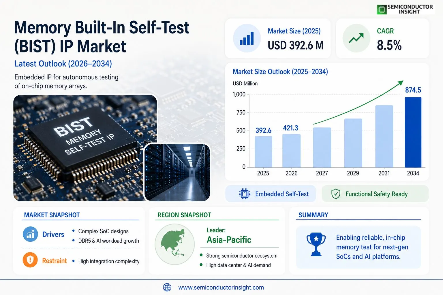
Global Memory Built-In Self-Test (BIST) IP market size was valued at USD 392.6 million in 2025. The market is projected to grow from USD 421.3 million in 2026 to USD 874.5 million by 2034, exhibiting a CAGR of 8.5% during the forecast period.
Memory BIST IP refers to embedded intellectual property cores integrated directly into semiconductor devices to enable autonomous, self-contained testing of memory arrays , including SRAM, DRAM, Flash, and embedded memory , without requiring external test equipment. These IP solutions encompass algorithms, controller logic, and diagnostic engines that execute test patterns, detect faults, perform repair analysis, and deliver pass/fail results, making them indispensable in modern system-on-chip (SoC) design and verification flows.
The market is gaining strong momentum driven by the rapid proliferation of complex SoCs across automotive, consumer electronics, artificial intelligence, and high-performance computing applications, where memory reliability and functional safety are non-negotiable. Furthermore, stringent compliance requirements such as ISO 26262 for automotive functional safety are compelling semiconductor designers to embed robust memory test capabilities at the IP level. Leading IP providers including Synopsys, Inc., Cadence Design Systems, and Siemens EDA are actively expanding their Memory BIST IP portfolios to address the growing complexity of advanced-node designs at 5nm and below.
MARKET DRIVERS
Rising Complexity of Semiconductor Designs Accelerating Demand for Memory BIST IP
The semiconductor industry is witnessing an unprecedented surge in chip complexity, with modern system-on-chip (SoC) designs integrating billions of transistors and multiple embedded memory arrays. This architectural evolution is a primary driver for Memory Built-In Self-Test (BIST) IP Market, as traditional external testing approaches are no longer sufficient to ensure memory reliability at advanced process nodes. Memory BIST IP enables on-chip, automated testing of embedded SRAM, DRAM, flash, and other memory types, significantly reducing test time and improving fault detection coverage. As chipmakers transition to 5nm, 3nm, and sub-3nm process technologies, the density and criticality of embedded memories have grown, making Memory BIST IP an indispensable component of any robust design-for-testability (DFT) strategy.
Proliferation of AI, Automotive, and Data Center Applications Fueling Market Growth
The rapid expansion of artificial intelligence processors, autonomous vehicle systems, and hyperscale data center infrastructure is creating sustained demand for reliable embedded memory solutions. These application domains are characterized by stringent functional safety requirements and zero-defect quality expectations, making Memory Built-In Self-Test (BIST) IP a critical enabler. Automotive chips, for instance, must comply with ISO 26262 functional safety standards, which mandate rigorous in-field memory testing , a requirement that Memory BIST IP fulfills efficiently through its ability to perform both manufacturing and in-system self-test routines. Similarly, AI accelerators and data center ASICs rely on large embedded memory arrays whose integrity must be continuously verified to sustain system uptime and computational accuracy.
➤ As semiconductor manufacturers increasingly adopt chiplet-based architectures and 2.5D/3D integration, the need for granular, IP-level memory testing solutions such as Memory BIST IP is expected to intensify, reinforcing its role as a foundational element of advanced chip validation flows.
Furthermore, Global push toward edge computing and IoT device proliferation is expanding the addressable base for Memory BIST IP beyond high-performance computing into power-constrained, cost-sensitive designs. Vendors offering scalable, low-power Memory BIST IP cores that can be customized for diverse memory architectures are well-positioned to capture growing opportunities across both established and emerging end-use segments.
MARKET CHALLENGES
Integration Complexity and Verification Overhead Posing Significant Challenges for Memory BIST IP Adoption
Despite its clear functional advantages, the integration of Memory Built-In Self-Test (BIST) IP into complex SoC environments introduces non-trivial engineering challenges. Design teams must carefully manage the interaction between BIST controllers and the surrounding memory subsystem, clock domain crossings, and scan chain architectures to avoid conflicts that could compromise test coverage or chip functionality. The verification of Memory BIST IP itself requires dedicated simulation environments and formal verification flows, adding to overall project timelines and resource requirements. Smaller semiconductor design houses with limited DFT expertise may find the adoption curve steep, particularly when targeting multiple memory types within a single design.
Other Challenges
Keeping Pace with Evolving Memory Architectures
Memory BIST IP Market must continuously evolve to support new and emerging memory technologies, including HBM, LPDDR5X, MRAM, and RRAM, each presenting distinct test algorithm requirements and fault models. IP vendors face the ongoing challenge of updating their offerings to maintain compatibility with the latest memory specifications while ensuring backward support for legacy designs, placing considerable pressure on R&D investment cycles and time-to-market commitments.
Licensing and Cost Barriers for Fabless Companies
The commercial licensing models for Memory BIST IP can represent a meaningful cost burden, particularly for early-stage fabless semiconductor companies operating under constrained budgets. Royalty-based and upfront licensing fees, when combined with the cost of integration support and customization services, may discourage adoption among price-sensitive customers. This dynamic creates a challenge for IP vendors in broadening their customer base while sustaining the R&D investments necessary to keep their Memory BIST IP portfolios competitive and standards-compliant.
MARKET RESTRAINTS
Limitations of Standardized BIST Algorithms Across Heterogeneous Memory Types
One of the inherent restraints affecting Memory Built-In Self-Test (BIST) IP Market is the difficulty of applying generalized test algorithms uniformly across diverse memory architectures. Standard march-based algorithms, while effective for conventional SRAM, may not provide adequate fault coverage for emerging non-volatile memory technologies with unique failure mechanisms. This technical gap necessitates the development of memory-type-specific BIST algorithms, increasing design complexity and customization requirements. IP vendors that cannot offer sufficiently adaptable or configurable BIST solutions risk losing design wins to competitors with more targeted offerings, limiting market penetration in specialized memory segments.
Area and Power Overhead Constraining Deployment in Resource-Limited Designs
The implementation of Memory BIST IP inherently introduces additional silicon area and power consumption, which can be a significant restraint in designs where both resources are tightly budgeted. In power-sensitive applications such as wearables, implantable medical devices, and ultra-low-power IoT endpoints, even modest BIST overhead may be difficult to accommodate without compromising the primary device specifications. While leading IP vendors have made progress in minimizing BIST footprint through algorithmic optimization and hardware sharing strategies, the area-power tradeoff continues to limit the addressable market, particularly at the low end of the performance and cost spectrum where Memory Built-In Self-Test (BIST) IP adoption remains relatively constrained.
MARKET OPPORTUNITIES
Functional Safety Mandates in Automotive and Industrial Sectors Creating Expanded Opportunities
The tightening of functional safety regulations across automotive and industrial electronics sectors presents a compelling growth opportunity for Memory Built-In Self-Test (BIST) IP Market. Regulatory frameworks such as ISO 26262 for automotive and IEC 61508 for industrial systems explicitly require in-system, periodic self-testing of safety-critical hardware elements, including embedded memories. This regulatory tailwind is driving semiconductor suppliers and Tier-1 automotive electronics manufacturers to mandate Memory BIST IP inclusion as a standard design requirement, expanding the total addressable market significantly. IP providers capable of delivering automotive-grade, ASIL-D compliant Memory BIST IP with documented diagnostic coverage metrics are positioned to benefit disproportionately from this structural demand shift.
Chiplet Ecosystems and Heterogeneous Integration Opening New Frontiers for BIST IP Deployment
The accelerating industry transition toward chiplet-based design methodologies and advanced packaging technologies such as 2.5D interposers and 3D stacking is creating a new frontier of opportunity for Memory Built-In Self-Test (BIST) IP providers. In disaggregated architectures, individual chiplets containing embedded memory must be independently testable before and after integration, elevating the strategic importance of embedded BIST solutions that can operate autonomously without reliance on external test infrastructure. Standards initiatives such as UCIe (Universal Chiplet Interconnect Express) and IEEE P2994 are beginning to formalize chiplet-level test interfaces, and Memory BIST IP that aligns with these emerging standards will gain strong adoption momentum as ecosystem players seek interoperable, scalable test solutions for heterogeneous integration platforms.
Growing Emphasis on In-Field Reliability Monitoring Driving Demand for Advanced Memory BIST Capabilities
Beyond manufacturing test, there is a growing market opportunity tied to the use of Memory BIST IP for in-field reliability monitoring and predictive maintenance applications. As semiconductor devices are deployed in mission-critical environments , including aerospace systems, medical equipment, and telecommunications infrastructure , the ability to continuously or periodically assess embedded memory health during system operation is gaining strategic importance. Memory Built-In Self-Test (BIST) IP with in-system test (IST) capabilities enables device operators to detect early-stage wear-out mechanisms, soft error accumulation, and retention failures before they escalate into system-level faults. This emerging use case broadens the value proposition of Memory BIST IP well beyond the traditional manufacturing test domain, opening sustained commercial opportunities for IP vendors investing in next-generation, runtime-capable BIST architectures.
Trends
Rising Demand for Embedded Memory Test Solutions Across Advanced-Node SoC Designs
Memory Built-In Self-Test (BIST) IP Market is experiencing accelerating momentum as semiconductor designers increasingly adopt embedded test methodologies to address the growing complexity of system-on-chip (SoC) architectures. As chip designs advance to 5nm process nodes and below, the density and criticality of on-chip memory arrays , including SRAM, DRAM, Flash, and embedded memory , have intensified the demand for autonomous, self-contained memory testing capabilities. Memory BIST IP solutions, which integrate controller logic, diagnostic engines, and fault-detection algorithms directly into the chip, are becoming foundational components of modern SoC design and verification flows. This trend is particularly pronounced in high-performance computing and artificial intelligence applications, where memory reliability directly impacts overall system integrity and operational efficiency.
Other Trends
Automotive Functional Safety Requirements Driving Adoption
Stringent compliance mandates such as ISO 26262 for automotive functional safety are compelling semiconductor designers to embed robust memory test capabilities at the IP level. As vehicles incorporate increasingly sophisticated electronic control units and advanced driver-assistance systems, the requirement for dependable memory verification within automotive-grade SoCs has intensified. Memory BIST IP enables automakers and their semiconductor supply chain partners to achieve the fault coverage and diagnostic accuracy necessary to meet functional safety integrity levels, making it a critical design requirement rather than an optional enhancement in the automotive segment.
Expansion of IP Portfolios by Leading Vendors
Major intellectual property providers including Synopsys, Inc., Cadence Design Systems, and Siemens EDA are actively broadening their Memory BIST IP portfolios to address evolving design challenges at advanced process nodes. These vendors are developing increasingly sophisticated solutions capable of executing complex test patterns, performing repair analysis, and delivering granular diagnostic results with minimal area and power overhead. The competitive landscape is being shaped by the ability of IP providers to support a wider range of memory types and process technologies while ensuring compatibility with established SoC design and verification ecosystems.
Proliferation of AI and High-Performance Computing Applications Accelerating Market Growth
The rapid proliferation of artificial intelligence accelerators and high-performance computing platforms is emerging as a significant growth catalyst for Memory Built-In Self-Test (BIST) IP Market. These application domains demand exceptionally high memory bandwidth and reliability, placing greater emphasis on comprehensive in-silicon memory testing throughout the device lifecycle. As AI chip architectures incorporate increasingly large and complex memory subsystems, Memory BIST IP is evolving from a post-silicon validation tool into an integral component of in-field monitoring and runtime diagnostics, supporting the long-term reliability requirements of data center and edge AI deployments.
COMPETITIVE LANDSCAPE
Key Industry Players
Memory Built-In Self-Test (BIST) IP Market: Competitive Dynamics and Leading Innovators Shaping the Future of Semiconductor Test IP
Global Memory Built-In Self-Test (BIST) IP market is characterized by a concentrated competitive structure dominated by a handful of established electronic design automation (EDA) and semiconductor IP giants. Synopsys, Inc. holds a commanding position in this space, leveraging its comprehensive DesignWare Memory BIST IP portfolio that supports advanced-node SoC designs at 5nm and below, offering robust fault detection, repair analysis, and ISO 26262-compliant functional safety capabilities. Cadence Design Systems and Siemens EDA (formerly Mentor Graphics) closely follow, each offering tightly integrated Memory BIST solutions embedded within their broader design and verification ecosystems. These leaders continuously invest in R&D to address the escalating complexity of SRAM, DRAM, Flash, and embedded memory testing across automotive, AI, and high-performance computing applications, where the stakes for memory reliability are exceptionally high. The competitive advantage in this market is primarily driven by algorithm sophistication, compatibility with leading foundry process nodes, integration with DFT (Design for Test) toolchains, and demonstrated compliance with automotive and functional safety standards.
Beyond the Tier-1 EDA leaders, several specialized IP vendors and emerging players contribute meaningfully to the Memory BIST IP competitive landscape. Companies such as Tessent (a Siemens EDA product line), Arm Holdings, and Arteris IP address niche but growing segments, including embedded memory testing for edge AI SoCs and automotive-grade chiplets. ANSYS (Synopsis acquired), Faraday Technology, eMemory Technology, and Mobiveil offer complementary IP and test solutions that integrate with Memory BIST flows in specific process or application contexts. The market also sees active participation from regional semiconductor IP firms in Asia, particularly in Taiwan, South Korea, and China, as domestic chip design ecosystems mature and demand locally sourced, cost-competitive Memory BIST solutions. Strategic partnerships between IP providers and leading foundries such as TSMC and Samsung Foundry further shape competitive positioning, as foundry-qualified Memory BIST IP becomes a key differentiator for SoC design teams targeting high-volume production.
List of Key Memory BIST IP Companies Profiled
- Synopsys, Inc.
- Cadence Design Systems
- Siemens EDA (Tessent)
- Arm Holdings
- Faraday Technology Corporation
- eMemory Technology Inc.
- Mobiveil Inc.
- Arteris IP
- LogicVision (acquired by Mentor/Siemens)
- ANSYS Inc.
- Springsoft (Cadence subsidiary)
- GUC (Global Unichip Corp.)
- Innosilicon Technology
- Dolphin Design
- VeriSilicon Holdings Co., Ltd.
Segment Analysis:
| Segment Category | Sub-Segments | Key Insights |
| By Type |
|
SRAM BIST IP holds a dominant position in Memory BIST IP Market owing to the widespread integration of SRAM arrays in virtually every modern system-on-chip design.
|
| By Application |
|
Automotive Electronics represents the most strategically critical application segment for Memory BIST IP, driven by increasingly rigorous functional safety standards and the rapid evolution of intelligent vehicle architectures.
|
| By End User |
|
Fabless Semiconductor Companies constitute the leading end-user segment for Memory BIST IP, reflecting a broader industry shift toward IP-based design methodologies that allow chipmakers to focus engineering resources on differentiated functionality rather than developing proprietary test infrastructure in-house.
|
| By Deployment Mode |
|
Soft IP (Synthesizable RTL-Based Cores) leads the deployment mode segment due to the unmatched flexibility and portability it offers across diverse semiconductor process technologies and design environments.
|
| By Test Methodology |
|
Repair-Assisted BIST with Built-In Self-Repair (BISR) Integration is the most strategically valued test methodology in the current market landscape, reflecting the growing imperative to maximize yield and extend operational lifetime in high-density memory arrays.
|
Regional Analysis: Memory Built-In Self-Test (BIST) IP Market
Asia-Pacific
Asia-Pacific hosts the world’s most concentrated cluster of semiconductor manufacturers and design firms, creating sustained demand for Memory Built-In Self-Test IP. Countries such as Taiwan and South Korea operate globally critical foundry and memory fabrication facilities, where embedded self-test solutions are essential for yield improvement and post-silicon validation across high-volume production environments.
The rapid expansion of automotive-grade chipsets and AI inference hardware across Asia-Pacific is significantly elevating the strategic importance of Memory BIST IP. Functional safety standards and performance reliability requirements in these verticals demand rigorous embedded memory testing protocols, prompting regional semiconductor design teams to prioritize advanced self-test intellectual property integration within their SoC architectures.
National semiconductor strategies across China, India, South Korea, and Japan are actively funding domestic chip design and verification capabilities. These policy frameworks accelerate the local development and licensing of Memory Built-In Self-Test IP solutions, reducing reliance on imported intellectual property while cultivating a generation of regionally capable EDA tool users and IP integrators.
Asia-Pacific’s leading foundries are aggressively migrating production to advanced process nodes, where embedded memory complexity rises sharply and conventional testing methods prove insufficient. This technological progression makes Memory BIST IP indispensable, as self-test routines embedded within chips dramatically reduce test time, improve defect coverage, and support in-field diagnostic capabilities across next-generation semiconductor devices.
North America
North America represents a highly mature and strategically influential market for Memory Built-In Self-Test (BIST) IP, anchored by the presence of world-leading semiconductor intellectual property developers, EDA software vendors, and fabless chip design companies concentrated primarily in the United States. Silicon Valley and broader technology corridors in Texas, Oregon, and Massachusetts host a dense network of design houses that integrate Memory BIST IP into complex system-on-chip architectures for applications spanning data centers, telecommunications infrastructure, aerospace, and defense electronics. The region’s stringent reliability and functional safety requirements, particularly within military and aerospace segments, place a premium on robust embedded memory self-test capabilities. Furthermore, the accelerating buildout of hyperscale data center infrastructure in North America is generating sustained demand for high-performance memory subsystems that incorporate advanced self-test intellectual property to ensure operational continuity. North America’s well-established IP licensing ecosystem and strong culture of semiconductor innovation position it as a critical hub for Memory Built-In Self-Test IP development and commercialization through the forecast horizon.
Europe
Europe occupies a strategically important position in Memory Built-In Self-Test (BIST) IP Market, distinguished by its strong orientation toward automotive semiconductor applications, industrial electronics, and safety-critical embedded systems. Germany, the Netherlands, France, and Sweden are home to prominent semiconductor design centers and Tier-1 automotive suppliers that demand rigorously tested memory subsystems compliant with ISO 26262 functional safety standards. The European emphasis on quality assurance and regulatory compliance in automotive and industrial applications creates a particularly compelling case for Memory BIST IP adoption, as embedded self-test mechanisms satisfy both production test efficiency and in-field diagnostic mandates. European semiconductor research initiatives, supported by the European Chips Act and collaborative R&D programs across member states, are progressively strengthening regional capabilities in advanced chip design and verification. This policy-driven momentum, combined with the region’s deep expertise in embedded systems and mixed-signal semiconductor design, ensures that Europe maintains a meaningful and growing role in shaping global Memory Built-In Self-Test IP demand patterns through 2034.
South America
South America remains an emerging participant in Global Memory Built-In Self-Test (BIST) IP Market, with its contribution primarily shaped by the gradual expansion of electronics manufacturing, telecommunications infrastructure modernization, and nascent semiconductor design activity concentrated in Brazil and, to a lesser extent, Argentina and Chile. While the region currently lacks the depth of semiconductor fabrication capability found in Asia-Pacific or North America, growing investments in digital infrastructure and the increasing adoption of locally assembled consumer electronics and IoT devices are slowly expanding the addressable market for Memory BIST IP solutions. Brazilian universities and technology institutes have begun cultivating semiconductor design expertise, and government-supported programs aimed at fostering a domestic electronics industry are laying foundational groundwork for future IP adoption. As regional original equipment manufacturers progressively adopt more sophisticated integrated circuit technologies, demand for embedded memory verification solutions, including Memory Built-In Self-Test IP, is anticipated to gain moderate traction across South America during the latter part of the forecast period.
Middle East & Africa
The Middle East and Africa region currently occupies an early-stage position within Global Memory Built-In Self-Test (BIST) IP Market, with demand primarily driven by telecommunications infrastructure expansion, smart city initiatives, and defense electronics modernization programs concentrated in Gulf Cooperation Council nations, particularly the United Arab Emirates, Saudi Arabia, and Israel. Israel stands out as a uniquely advanced semiconductor design hub within the broader region, hosting globally recognized chip design centers affiliated with multinational technology corporations that actively engage with Memory BIST IP for high-performance computing and communications applications. Gulf nations are channeling substantial sovereign investment into digital transformation agendas that indirectly stimulate demand for advanced semiconductor components incorporating self-test capabilities. While Africa’s contribution to the Memory Built-In Self-Test IP Market remains limited by constrained semiconductor infrastructure, the continent’s expanding mobile connectivity ecosystem and increasing electronics consumption suggest a gradual long-term demand trajectory. Overall, the Middle East and Africa region is expected to develop incrementally as a market for Memory Built-In Self-Test IP through the 2026 to 2034 forecast period.
Report Scope
This market research report provides a comprehensive analysis of the Memory Built-In Self-Test (BIST) IP Market , covering the forecast period 2026–2034. It offers detailed insights into market dynamics, technological advancements, competitive landscape, and key trends shaping the industry.
Key focus areas of the report include:
- Market Overview: The report begins with an overview outlining its current market scenario, key growth indicators, and industry transformation drivers. It discusses macroeconomic factors, demand–supply balance, regulatory landscape, and the strategic role of semiconductors in powering advancements across industries such as automotive, telecommunications, consumer electronics, and industrial automation.
- Market Size & Forecast: Historical data and future projections for revenue, unit shipments, and market value across major regions and segments.
- Segmentation Analysis: Detailed breakdown by product type, technology, application, and end-user industry to identify high-growth segments and investment opportunities.
- Regional Insights: Insights into market performance across North America, Europe, Asia-Pacific, Latin America, and the Middle East & Africa, including country-level analysis where relevant.
- Competitive Landscape: Profiles of leading market participants, including their product offerings, R&D focus, manufacturing capacity, pricing strategies, and recent developments such as mergers, acquisitions, and partnerships.
- Technology Trends & Innovation: Assessment of emerging technologies, integration of AI/IoT, semiconductor design trends, fabrication techniques, and evolving industry standards.
- Market Drivers & Restraints: Evaluation of factors driving market growth along with challenges, supply chain constraints, regulatory issues, and market-entry barriers.
- Stakeholder Insights: Insights for component suppliers, OEMs, system integrators, investors, and policymakers regarding the evolving ecosystem and strategic opportunities.
Primary and secondary research methods are employed, including interviews with industry experts, data from verified sources, and real-time market intelligence to ensure the accuracy and reliability of the insights presented.
FREQUENTLY ASKED QUESTIONS:
What is the current market size of Memory Built-In Self-Test (BIST) IP Market?
-> Global Memory Built-In Self-Test (BIST) IP Market was valued at USD 392.6 million in 2025 and is projected to grow from USD 421.3 million in 2026 to USD 874.5 million by 2034, exhibiting a CAGR of 8.5% during the forecast period.
Which key companies operate in Memory Built-In Self-Test (BIST) IP Market?
-> Key players include Synopsys, Inc., Cadence Design Systems, and Siemens EDA, among others, who are actively expanding their Memory BIST IP portfolios to address the growing complexity of advanced-node designs at 5nm and below.
What are the key growth drivers?
-> Key growth drivers include the rapid proliferation of complex SoCs across automotive, consumer electronics, artificial intelligence, and high-performance computing applications, where memory reliability and functional safety are critical. Stringent compliance requirements such as ISO 26262 for automotive functional safety are also compelling semiconductor designers to embed robust memory test capabilities at the IP level.
Which region dominates the market?
-> Asia-Pacific is the fastest-growing region, driven by strong semiconductor manufacturing activity, while North America remains a significant market led by major IP providers and advanced SoC design activity.
What are the emerging trends?
-> Emerging trends include integration of Memory BIST IP in advanced-node designs at 5nm and below, growing adoption in AI and high-performance computing SoCs, and increased focus on functional safety compliance such as ISO 26262 across automotive semiconductor applications.

Get Sample Report PDF for Exclusive Insights
Report Sample Includes
- Table of Contents
- List of Tables & Figures
- Charts, Research Methodology, and more...
 Download Sample Report PDF

