
Key Statistics
Key Takeaways
- Largest type – Vertical needle and MEMS probe cards lead advanced logic testing because they support dense arrays, high parallelism and controlled electrical performance.
- Fastest demand – AI accelerators and leading-edge logic create the strongest growth through larger die, more test content, higher currents and expensive downstream packaging.
- Largest region – Asia Pacific leads because most wafer fabrication, outsourced assembly and test, and major probe-card manufacturing capacity are concentrated in Taiwan, South Korea, Japan and China.
- Industry evidence – SEMI reported semiconductor test-equipment sales surged 55.3% in 2025 and projected a further 31.0% increase to USD 15.3 billion in 2026.
- Core restraint – Probe cards are custom interfaces with long qualification cycles; a design error or contact-yield problem can idle costly testers and delay wafer release.
- Competitive shift – Suppliers are combining MEMS probes, advanced PCBs, analyzers, repair and global application engineering to control more of the test-interface stack.
Logic Test Probe Card Market Overview
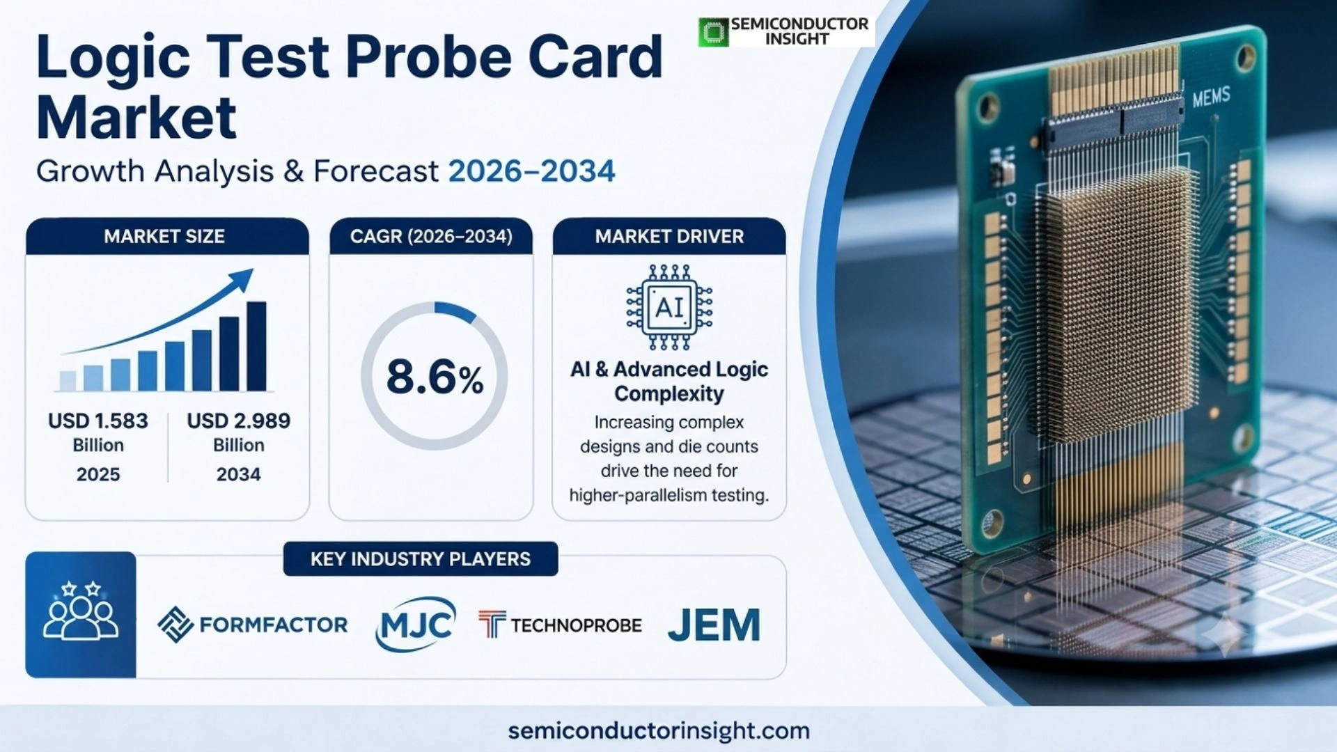
Logic Test Probe Card Market was valued at approximately USD 1.421 billion in 2025 and is projected to reach USD 2.989 billion by 2034, expanding at a 8.6% CAGR during 2026–2034. Asia Pacific is the largest market because logic wafers are predominantly fabricated and tested there, while AI and leading-edge logic are raising the technical and economic value of wafer-level test.
A logic test probe card is the electromechanical interface between automated test equipment, a wafer prober and the bond pads or bumps of multiple integrated circuits while they remain on the wafer. It routes test signals and power through a printed-circuit structure and microscopic probes, enabling defective die to be identified before dicing and packaging. The market includes probe-card assemblies, probe heads and closely associated application engineering, repair and refurbishment.
The scope is specifically logic-device wafer test and does not treat memory-only probe cards, packaged-device test sockets, ordinary bare printed circuit boards or complete automated test systems as equivalent products. This boundary is commercially important because a probe card is customized to pad layout, wafer diameter, tester interface, temperature, current, frequency and parallelism, giving design support and qualification capability a larger role than catalog pricing.
Market growth is reinforced by the rising cost of downstream advanced packaging. A defective AI or leading-edge logic die that escapes wafer sort can waste an expensive package and compromise a multi-die assembly. Probe cards therefore support known-good-die strategies and earlier defect detection. SEMI reported that semiconductor test-equipment sales rose 55.3% in 2025 and forecast a further 31.0% increase to USD 15.3 billion in 2026, evidence of an unusually strong test investment cycle.
Segment Analysis: By Type
By type, the supplied scope comprises vertical needle or tip, thin-film MLO and membrane logic test probe cards. Vertical architectures hold the largest advanced-logic position because MEMS and buckling-beam arrays can address dense layouts with high parallelism, while thin-film and membrane approaches remain relevant where short electrical paths, controlled impedance or application-specific contact structures outweigh mechanical complexity.
| Type | Technical function | Market position |
|---|---|---|
| Vertical Needle/Tip | Vertically arranged probes contact dense pad or bump arrays while the probe head controls planarity, scrub and force. MEMS fabrication improves dimensional repeatability and supports high parallelism. | Largest advanced-logic segment; favored for AI, processors and complex system-on-chip devices. |
| Thin Film MLO | A multilayer organic or thin-film space transformer distributes high-density signals between tester-side connections and the probe array. Electrical design is critical for power delivery and signal integrity. | High-value enabling structure used within sophisticated probe-card assemblies rather than a simple commodity category. |
| Membrane Logic Test Probe Card | Flexible or membrane-based contact structures provide short signal paths and controlled electrical characteristics for suitable pad layouts and test conditions. | Application-specific segment selected where high-frequency behavior and customized contact geometry justify qualification effort. |
Pricing and service economics
Probe-card pricing rises with pin count, parallel sites, probe material, high-frequency performance, thermal range, current delivery and custom space-transformer complexity. The initial card is only part of lifecycle value: cleaning, repair, probe-head replacement, planarity restoration and rapid engineering changes affect tester utilization. Suppliers with nearby service centers can command preference because shortening repair turnaround protects far more valuable wafer and automated-test-equipment capacity.
Segment Analysis: By Application
The supplied page labels applications as SME and large enterprise, which is a buyer-size axis rather than a semiconductor-device application. Large enterprises dominate because leading foundries, integrated device manufacturers and outsourced test companies operate the highest-volume wafer-sort programs. Smaller and medium buyers participate through design houses, specialty fabs and regional test operations that prioritize flexible engineering support and manageable qualification cost.
| Application | Demand characteristics |
|---|---|
| SME | Smaller semiconductor companies and specialist test operations purchase lower volumes but often require intensive customization. They value responsive engineering, reuse of platform components, refurbishment and access to regional service because a delayed card can block an entire product qualification or low-volume production run. |
| Large Enterprise | Foundries, IDMs and OSATs operate many testers and demand high site parallelism, consistent contact performance and global support. Their volume supports co-development and long qualification programs, but it also creates strict supplier audits, second-source requirements and continuous pressure to reduce test cost per die. |
Regional Analysis
Asia Pacific is the largest and fastest-growing market because it combines the dominant concentration of wafer fabrication, outsourced assembly and test, semiconductor equipment supply and probe-card manufacturing. North America leads many advanced-logic designs and test architectures, Europe emphasizes automotive and industrial reliability, while South America and Middle East and Africa remain small markets centered on design, research and emerging packaging initiatives.
How does regional demand differ across the logic test probe card market?
Probe cards are consumed where wafers are tested, but technical specifications often originate where chips are designed. Asia Pacific therefore captures the largest physical demand and service workload; North America influences high-end designs through AI and processor companies; Europe buys around automotive and industrial quality; South America has limited wafer-sort infrastructure; and Middle Eastern initiatives focus on research, design and potential future packaging rather than present mass production.
| Region | Position | Growth outlook | Demand profile | Supplier selection |
|---|---|---|---|---|
| Asia Pacific | Largest and fastest | Very high | Fab, foundry and OSAT concentration | Local co-development, repair turnaround and advanced MEMS capability |
| North America | Major technology centre | High | AI, CPU, GPU and specialty logic | Signal integrity, roadmap alignment and engineering access |
| Europe | Specialized | Moderate | Automotive, industrial and power-control logic | Reliability, temperature performance and lifecycle support |
| South America | Small | Selective | Design, research and limited manufacturing | Imported availability and application support |
| Middle East & Africa | Emerging | Long-term | Research, design and planned localization | Technology transfer, training and partner ecosystem |
Key Logic Test Probe Card Manufacturers and Competitive Landscape
The market is concentrated among suppliers with proprietary probe structures, advanced space transformers, deep application engineering and global repair networks. FormFactor, Micronics Japan and Technoprobe are central competitors, while JEM, MPI, SV Probe, TSE and regional specialists address particular technologies and customers. Competitive wins occur at device-program level and can persist through a product generation after qualification.
FormFactor competes across advanced probe cards and test interfaces with a broad installed base and global customer relationships. Technoprobe has strengthened its position in logic AI applications and expanded into adjacent advanced PCB capabilities through DIS Tech. MJC combines probe cards with probers and test equipment and reported record probe-card sales, while JEM contributes Japanese precision manufacturing and long-standing wafer-test expertise.
Qualification creates switching costs because a replacement card must reproduce contact, electrical and thermal behavior without disrupting yield. However, major customers also pursue second sourcing to protect production continuity. Suppliers therefore balance proprietary technology with the need to match tester, prober and device roadmaps. Local repair centers, spare probe heads and data-driven maintenance can be as decisive as the original card architecture.
| Competitive tier | Companies | Basis of competition |
|---|---|---|
| Global leaders | FormFactor; Micronics Japan; Technoprobe | MEMS technology, advanced logic programs, global engineering and repair footprint. |
| Established specialists | Japan Electronic Materials; MPI Corporation; SV Probe; TSE | Application-specific probe architectures, regional customer access and technical support. |
| Regional and niche suppliers | Microfriend; Korea Instrument; Feinmetall; Synergie Cad Probe; Will Technology | Cost, local responsiveness, specialty contact technology and mature-node programs. |
| Test ecosystem participants | Advantest; STAr Technologies; TIPS Messtechnik; CHPT | Adjacent test equipment, boards, analysis or regional interface capability. |
Key companies profiled
- FormFactor
- Micronics Japan (MJC)
- Technoprobe S.p.A.
- Japan Electronic Materials (JEM)
- MPI Corporation
- SV Probe
- Microfriend
- Korea Instrument
- Feinmetall
- Synergie Cad Probe
- Advantest
- Will Technology
- TSE
- TIPS Messtechnik GmbH
- STAr Technologies, Inc.
- and CHPT
Probe Technology and Manufacturing Capability Analysis
Manufacturing capability is strategically important because logic probe cards combine precision probes, multilayer substrates, printed-circuit assemblies and demanding metrology. Capacity cannot be measured only by factory floor area: usable output depends on design engineers, MEMS process yield, space-transformer availability, assembly skill, metrology, customer qualification and the ability to repair cards near production fabs.
Advanced cards require micron-scale dimensional control across hundreds or thousands of contacts. Probe formation, lithography, plating, ceramic or organic substrate processing, precision assembly and planarity adjustment must collectively meet electrical and mechanical specifications. Expanding physical capacity without maintaining yield can raise cost and lead time. MJC’s plan to improve capacity at its Aomori factory and release a vertical MEMS logic card illustrates the coupling between product technology and manufacturing readiness.
Regional service capacity is another effective production constraint. Cards wear, contaminate or require modification as wafer processes and test programs change. A supplier that can diagnose and repair locally returns the interface to production faster and reduces the number of spare cards a customer must hold. Consequently, investment in service centers, analyzers and trained field engineers expands addressable demand even when it does not add new-card assembly lines.
Logic Test Probe Card Market Dynamics: Drivers, Restraints and Opportunities
Demand is driven by AI and advanced logic complexity, rising test content, expensive downstream packaging and global fab investment. Restraints include custom development cost, long qualification, contact-yield risk and cyclical tester utilization. Opportunities lie in high-parallelism MEMS cards, known-good-die testing for chiplets, integrated probe-card analytics, regional repair and broader test-interface portfolios.
MARKET DRIVERS
Drivers Impact Analysis*
| Factor | Directional impact on CAGR forecast | Geographic relevance | Time horizon |
|---|---|---|---|
| AI and advanced logic complexity | +2.8% | North America and Asia Pacific | Immediate |
| Higher wafer-sort test content | +1.9% | Global leading-edge fabs | Short term |
| Known-good-die economics | +1.5% | Advanced packaging hubs | Medium term |
| Fab and test-equipment investment | +1.2% | Asia Pacific, US and Europe | Short to medium term |
AI accelerators increase pins, current and test complexity
AI and high-performance logic devices combine large die, dense interfaces and demanding power delivery. Wafer sort must exercise more functions at higher parallelism while preserving signal integrity and contact stability. Technoprobe linked its 2025 performance to a leading position in logic AI chip testing, showing that technical complexity translates into commercial demand for higher-value probe cards rather than merely more units of conventional interfaces.
Rising test content increases probe-card utilization
New transistor architectures, high-speed interfaces and heterogeneous integration create more tests and tighter guard bands. More test seconds per wafer raise the value of parallel site testing, stable contact resistance and rapid card maintenance because interface problems directly consume expensive tester time. Suppliers that enable more devices to be tested simultaneously can improve customer cost per die and justify premium designs despite higher initial card prices.
Advanced packaging makes early defect detection more valuable
Chiplet and multi-die packages combine several valuable components after wafer fabrication. If one defective die enters the assembly, packaging cost and other known-good components may be lost. Logic probe cards enable earlier screening and characterization, making known-good-die confidence an economic requirement. This expands demand for accurate wafer-level test across compute dies, I/O dies and other logic components destined for advanced packages.
The semiconductor test investment cycle supports demand
SEMI reported global semiconductor test-equipment sales increased 55.3% in 2025 and projected 31.0% growth to USD 15.3 billion in 2026. Probe cards are not equivalent to automated test equipment, but the figures demonstrate customer investment in wafer and device test capacity. New testers and expanded wafer-sort programs create opportunities for compatible cards, analyzers, repair and application engineering.
MARKET RESTRAINTS
Restraints Impact Analysis*
| Factor | Directional impact on CAGR forecast | Geographic relevance | Time horizon |
|---|---|---|---|
| Custom design and qualification cost | -1.5% | Global advanced logic | Immediate |
| Contact yield and maintenance risk | -1.1% | High-volume fabs | Ongoing |
| Semiconductor cyclicality | -0.9% | Global | Short to medium term |
| Concentrated specialist skills | -0.6% | Emerging manufacturing regions | Medium term |
Every device program requires customized engineering
Pad layout, tester resources, wafer prober, operating temperature, current, frequency and parallelism vary by product. A probe card therefore needs application-specific electrical and mechanical design followed by customer qualification. Development expense and lead time can be difficult for small-volume programs, while late device changes may require redesign. This limits true catalog standardization and makes forecast accuracy important for both buyer and supplier.
Contact performance directly affects yield and tester uptime
Probe contamination, wear, planarity drift or unstable contact resistance can create false fails and reduce productive tester hours. Because the card touches every die tested, a small interface problem can have factory-wide financial consequences. Customers mitigate the risk with cleaning schedules, preventive maintenance, spares and supplier repair support, but these requirements raise lifecycle cost and slow adoption of unfamiliar probe technologies.
Cyclical wafer demand can leave custom capacity underutilized
Probe-card suppliers invest in MEMS processes, substrate capability and skilled engineering ahead of customer ramps. If a smartphone, automotive or data-centre cycle weakens, production programs can be delayed while fixed costs remain. AI-related demand currently supports advanced logic, yet concentration in a small number of large programs creates volatility. Diversified customer exposure and repair revenue can soften, but not eliminate, this cyclicality.
MARKET OPPORTUNITIES
High-parallelism vertical MEMS cards
Foundries and OSATs seek lower test cost per die as wafer volumes and test content increase. Vertical MEMS arrays can support dense contacts and multiple devices tested in parallel, converting precision manufacturing into customer throughput. Suppliers with strong probe uniformity, space-transformer design and planarity control can capture premium programs, particularly in AI accelerators and system-on-chip devices where test economics justify sophisticated interfaces.
Chiplet and known-good-die test strategies
Heterogeneous integration creates new points at which logic die must be screened, characterized and sometimes tested at multiple temperatures before assembly. Probe-card makers can co-develop interfaces for compute chiplets, I/O dies and wafer-level interconnect structures. The opportunity extends beyond card revenue to engineering, characterization hardware and analytics that help customers define effective screening without adding unnecessary test time.
Digital diagnostics and preventive maintenance
Probe-card analyzers and statistical monitoring can identify damaged probes, contact drift or electrical faults before they interrupt production. Technoprobe’s Athena platform supports deep debug and 100% tests, with configurations for high-volume statistical data collection. Connecting analyzer data to repair planning can create service revenue, improve spare-card allocation and strengthen supplier relationships by demonstrating measurable gains in availability and yield stability.
Regional repair and engineering centers
As wafer fabrication expands beyond established hubs, customers need local cleaning, repair, planarity and application support. Establishing service capability requires less capital than a complete probe-card factory but can materially reduce customer downtime. Suppliers can use regional centers to win mature-node and specialty programs first, then add design and assembly capability as volumes justify investment, creating a staged market-entry path.
Logic Probe Card Value-Chain Analysis
The value chain runs from semiconductor device and test-program definition through probe and substrate manufacture, card assembly and metrology, customer qualification, wafer-sort operation and recurring repair. Technical information flows upstream from device designers, while cards and service flow toward fabs and OSATs. The most defensible value pools are proprietary probe technology, high-density interconnect design and rapid local support.
Concentration risk exists in proprietary probe processes, advanced multilayer substrates and expert application engineering. Strategic partnerships can secure critical PCBs and expand interface capability, as illustrated by the Technoprobe–Advantest agreement. Customers reduce exposure through second sourcing and spare cards, but exact interchangeability is difficult after qualification. Suppliers that control more layers of the stack can shorten root-cause analysis and capture a larger share of lifecycle spending.
Recent Developments in the Logic Test Probe Card Market
Developments tracked to September 2026. Entries are dated to their official announcement or publication period.
- July 2026
Source, up 31.0% after a 55.3% increase in 2025. The acceleration supports new wafer-sort capacity and higher utilization of advanced probe interfaces for AI-related logic. - November 2025
Source, 20.6% above the prior-year period, and highlighted its position in logic AI chip testing. The result provides company-level evidence that AI test complexity is supporting demand for advanced interfaces. - January 2025
Source covering priority supply of probe-card PCBs, test-board PCBs and related solutions. The agreement tightens the relationship between probe technology and critical interconnect substrates and may improve supply coordination. - 2025
Source, noting higher non-memory probe-card sales through new customers and new products despite a gradual automotive recovery. The statement indicates broader logic-card momentum rather than dependence on memory demand alone.
REPORT SCOPE & SEGMENTATION
| Attribute | Details |
|---|---|
| Category | Semiconductor Equipment > Test & Measurement > Wafer Probe Cards |
| Base year | 2025 |
| Forecast period | 2026–2034 |
| Market size | USD 1.421 billion in 2025; USD 2.989 billion by 2034; 8.6% CAGR |
| By Type | Vertical Needle/Tip; Thin Film MLO; Membrane Logic Test Probe Card |
| By Application | SME; Large Enterprise |
| Regions | North America; Europe; Asia Pacific; South America; Middle East & Africa |
| Companies | FormFactor; Micronics Japan (MJC); Technoprobe S.p.A.; Japan Electronic Materials (JEM); MPI Corporation; SV Probe; Microfriend; Korea Instrument; Feinmetall; Synergie Cad Probe; Advantest; Will Technology; TSE; TIPS Messtechnik GmbH; STAr Technologies, Inc.; CHPT |
Frequently Asked Questions
What is the current size of the logic test probe card market?
The global logic test probe card market was valued at approximately USD 1.421 billion in 2025. The market covers electromechanical interfaces used between automated test equipment, wafer probers and logic devices while those devices remain on the wafer. It includes probe-card assemblies, probe heads and associated engineering and lifecycle service, while excluding complete testers and packaged-device sockets.
What will the market be worth by 2034?
The market is projected to reach approximately USD 2.989 billion by 2034, expanding at a 8.6% CAGR during 2026–2034. Growth is supported by AI accelerators, rising logic test content, high-parallelism wafer sort, more expensive downstream advanced packaging and continued investment in semiconductor test equipment and fabrication capacity. These forces increase both the number and technical value of qualified card programs.
Which region leads the logic test probe card market?
Asia Pacific is the largest market because Taiwan, South Korea, Japan and China concentrate a large share of global wafer fabrication, outsourced semiconductor assembly and test, and probe-card manufacturing. Proximity matters because customized cards require application engineering, cleaning and repair, so suppliers with local technical centers can protect customer tester uptime and production schedules.
What is a logic test probe card?
A logic test probe card is a customized interface that routes electrical signals and power between automated test equipment and microscopic pads or bumps on integrated circuits before the wafer is diced. It allows defective die to be identified early, supports parametric and functional measurements and helps prevent packaging cost from being spent on devices that do not meet specification.
Which product type leads the market?
Vertical needle and vertical MEMS architectures lead advanced logic applications because they can address dense contact arrays, deliver controlled scrub and force, and support greater test parallelism. Thin-film MLO and membrane structures remain important for applications requiring specialized routing, controlled impedance or short electrical paths, but selection depends on the exact device and tester configuration.
What is driving market growth?
AI and leading-edge logic devices require more pins, higher currents, tighter signal integrity and greater test coverage. At the same time, chiplet and multi-die packaging raises the cost of allowing a defective die to escape wafer sort. These requirements increase the technical value of probe cards and encourage customers to invest in parallelism, diagnostics and reliable local service.
What are the main restraints?
Custom engineering cost, lengthy qualification, contact-yield risk, semiconductor cyclicality and a limited pool of precision manufacturing and application specialists restrain the market. Because a probe card touches every tested die, contamination or planarity errors can generate false failures and consume expensive tester capacity, prompting conservative qualification and second-source strategies among major customers.
Which companies are profiled?
The report profiles FormFactor, Micronics Japan, Technoprobe, Japan Electronic Materials, MPI Corporation, SV Probe, Microfriend, Korea Instrument, Feinmetall, Synergie Cad Probe, Advantest, Will Technology, TSE, TIPS Messtechnik, STAr Technologies and CHPT. The competitive analysis distinguishes core probe-card manufacturers from adjacent test-equipment, board and interface participants and compares their engineering, manufacturing, qualification and regional-service roles.
Why is local service strategically important?
Probe cards require cleaning, repair, planarity restoration and occasional engineering modification throughout their operating life. A distant repair loop can leave valuable automated test equipment idle or force the customer to carry more spare cards. Local centers shorten turnaround, improve root-cause communication and give suppliers a practical path to enter growing semiconductor regions before building full manufacturing capacity.
How does AI affect the market?
AI accelerators and associated processors are large, power-intensive logic devices with demanding high-speed interfaces and costly packaging. Their wafer-sort programs need stable power delivery, dense contact arrays, strong signal integrity and high parallelism. Technoprobe’s reported strength in logic AI chip testing and SEMI’s sharp test-equipment growth figures show how AI investment is propagating into the test-interface ecosystem.
Get Sample Report PDF for Exclusive Insights
Report Sample Includes
- Table of Contents
- List of Tables & Figures
- Charts, Research Methodology, and more...






Be the first to review “Logic Test Probe Card Market, Size, Share, Trends, Market Growth and Forecast 2026-2034”