Key Statistics
Key Takeaways
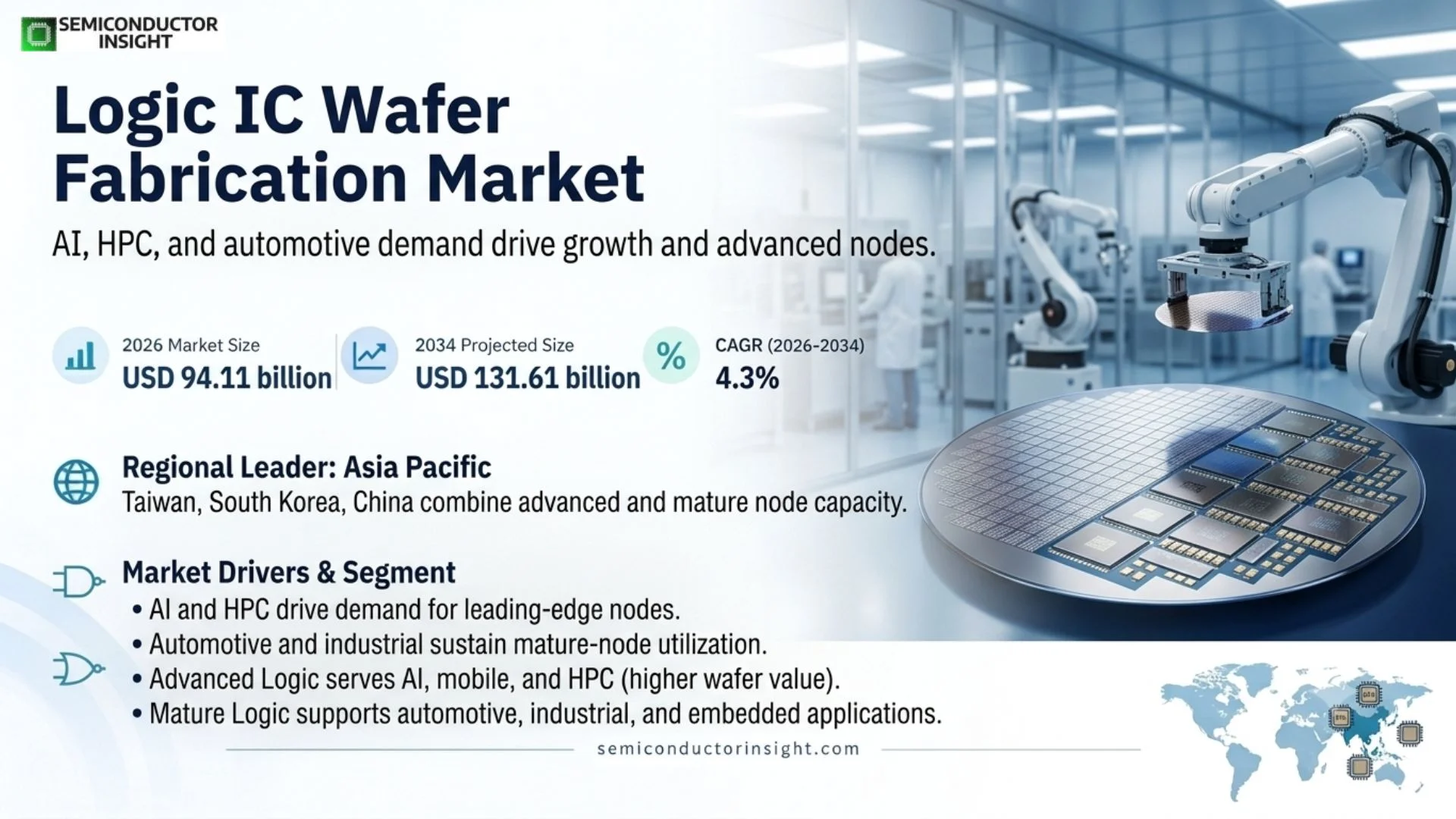
- Market size: The market stands at USD 90.25 billion in 2025 and is projected to reach USD 131.61 billion by 2034, representing a 4.3% CAGR across 2026–2034.
- Advanced logic below 28nm drives the highest-value growth through AI accelerators, CPUs, GPUs, networking silicon and premium mobile SoCs, while mature logic remains essential for automotive and industrial devices.
- Asia Pacific leads fabrication because Taiwan, South Korea and China host the most concentrated foundry capacity and semiconductor manufacturing infrastructure.
- Pure-play foundries continue gaining strategic influence as fabless customers outsource capital-intensive manufacturing and rely on specialist process, yield and packaging ecosystems.
- 2nm production and global fab localization are reshaping capacity, but cost, yield and customer qualification keep leading-edge manufacturing concentrated among a small number of suppliers.
Logic IC Wafer Fabrication Market Overview
Logic IC Wafer Fabrication Market is valued at USD 90.25 billion in 2025 and is projected to reach USD 131.61 billion by 2034, expanding at a 4.3% CAGR during 2026–2034. The 2026 market level is USD 94.11 billion. Asia Pacific leads global logic fabrication because Taiwan, South Korea and China combine advanced-node foundries, mature-node capacity, packaging and dense electronics supply chains. AI and high-performance computing are increasing leading-edge demand, while automotive and industrial customers sustain mature-node utilization. The market is expanding through both technology migration and geographic diversification of manufacturing.
Logic IC wafer fabrication converts customer or internal circuit designs into patterned silicon wafers through lithography, deposition, etch, implantation, anneal, clean and metallization steps. The market includes advanced logic processes below 28nm and mature logic processes above 28nm across pure-play foundries and integrated device manufacturers. Revenue depends on wafer volume, process node, mask complexity, yield, wafer diameter and the value of specialty options integrated into a process platform.
Leading-edge logic is moving from FinFET toward gate-all-around nanosheet transistors, backside power delivery and increasingly complex EUV patterning. TSMC states that its 2nm technology entered high-volume manufacturing in the fourth quarter of 2025 and that 3nm represented 24% of wafer revenue in 2025. Mature nodes remain critical because automotive, industrial and connectivity products often prioritize reliability, embedded analog or long lifecycle over maximum transistor density.
The business model splits between pure-play foundries and IDMs. Pure-play foundries monetize process technology, scale, yield and customer confidentiality across many fabless customers, while IDMs combine product design and manufacturing. Customers evaluate foundries on PPA, yield, cycle time, capacity reservation, advanced packaging access and geographic resilience. Leading-edge economics favor large scale because a modern fab requires enormous capital and must maintain high utilization to recover equipment costs.
Segment Analysis: By Type
By type, the market is segmented into advanced logic processes below 28nm and mature logic processes above 28nm. Advanced logic commands higher wafer value and serves AI, mobile and high-performance computing, while mature logic supports automotive, industrial, analog-mixed-signal and cost-sensitive embedded applications. Both segments remain commercially important because end markets have different performance, qualification and lifecycle requirements.
| Type | Technical / commercial role | Market position |
|---|---|---|
| Advanced Logic Process (Below 28nm) | FinFET and GAA-based nodes used for AI processors, CPUs, GPUs, mobile SoCs and networking silicon. | Highest-value growth segment with intense R&D, EUV and advanced packaging requirements. |
| Mature Logic Process (Above 28nm) | Planar and mature process platforms for automotive, industrial, connectivity and embedded logic. | Large installed base with strong lifecycle, cost and specialty-process advantages. |
Additional Segmentation: By End User
End users include IDMs, fabless semiconductor companies and system OEMs developing custom silicon. Fabless companies are the core customers of pure-play foundries and increasingly depend on external manufacturing for advanced nodes. System OEMs and hyperscalers are becoming more important as custom AI and infrastructure chips move from merchant silicon toward application-specific designs, increasing direct engagement with foundry ecosystems.
| End User | Demand characteristics |
|---|---|
| IDMs | Companies that combine chip design and manufacturing but may also use external foundry capacity for selected products or nodes. |
| Fabless Semiconductor Companies | Primary foundry customers that outsource wafer manufacturing while retaining architecture and product design. |
| System OEMs | Cloud, automotive and electronics companies designing custom chips and working directly with foundry ecosystems. |
Segment Analysis: By Application
By application, computing and data centers show the strongest value growth because AI and cloud workloads require advanced CPUs, GPUs, accelerators and networking silicon. Consumer electronics remains a large volume market, automotive supports both mature and advanced logic, industrial automation favors long-lived and mixed-signal-capable platforms, and telecommunications uses leading and mature nodes across infrastructure and connectivity.
| Application | Demand characteristics |
|---|---|
| Computing & Data Centers | AI accelerators, CPUs, GPUs and networking silicon drive leading-edge wafer demand and advanced packaging. |
| Consumer Electronics | Smartphone, PC and smart-device SoCs combine high volumes with rapid node migration. |
| Automotive Electronics | ADAS, central compute, connectivity and MCU-adjacent logic use both advanced and mature process platforms. |
| Industrial Automation | Long-lifecycle control and edge systems favor proven nodes, specialty options and supply continuity. |
| Telecommunications | Baseband, networking and optical-transport silicon require high performance, connectivity and power efficiency. |
Additional Segmentation: By Business Model
The market is split between IDM and pure-play foundry models. IDMs manufacture their own product portfolios and can optimize process technology around internal devices, while pure-play foundries spread capital and R&D across many customers. The pure-play model has become especially influential at advanced nodes because few fabless companies can justify building leading-edge fabs independently, and scale improves utilization, process learning and packaging integration.
| Business Model | Commercial relevance |
|---|---|
| IDM | Integrated design and manufacturing with process capacity primarily supporting internal product roadmaps. |
| Pure-Play Foundry | Merchant manufacturing serving many fabless and system customers across shared process platforms. |
Regional Analysis
Asia Pacific leads because Taiwan, South Korea and China host the most concentrated foundry capacity, while Japan retains specialty manufacturing and packaging strengths. North America is expanding through U.S. leading-edge and mature-node projects, Europe is investing in automotive and specialty fabs, and other regions remain smaller. Regional share is determined by installed wafer capacity and process-node mix rather than end-device consumption.
Why does regional demand differ across the Logic IC Wafer Fabrication market?
Foundry economics reward dense ecosystems of equipment, materials, engineering talent and customers. Taiwan’s concentration supports rapid yield learning and advanced packaging, South Korea combines logic and memory manufacturing, and China continues investing in domestic capacity. U.S. and European fab expansion improves geographic resilience, but leading-edge manufacturing remains difficult to replicate quickly because technology transfer, ramp yield and workforce development take years.
| Region | Position | Growth outlook | Demand profile | Supplier selection |
|---|---|---|---|---|
| Asia Pacific | Largest | High | Manufacturing, design and end-market demand | Qualification, local support and scale |
| North America | High-value | High | Technology development and premium demand | Engineering support and platform access |
| Europe | Strategic | Steady-high | Automotive, industrial and specialty applications | Reliability, lifecycle and compliance |
| South America | Emerging | Moderate | Imported technology and project-led demand | Price, availability and distributor support |
| Middle East & Africa | Emerging | Selective | Infrastructure, research and premium applications | Project access and technical support |
Competitive Landscape
TSMC is the leading pure-play foundry, followed by Samsung Foundry, GlobalFoundries, UMC, SMIC and other regional manufacturers. Intel Foundry adds an IDM-origin merchant model, while Texas Instruments, STMicroelectronics, onsemi and Renesas maintain substantial internal manufacturing. Competitive differentiation centers on node leadership, yield, capacity, packaging, specialty options and customer trust. For commercial buyers, the practical decision therefore depends on qualification evidence, system-level performance, lifecycle support and supply continuity rather than a single headline specification.
Advanced-node competition is becoming more difficult because GAA transistors, EUV lithography and backside power require higher R&D and capital intensity. TSMC’s 2nm production ramp and planned N2P and A16 variants show how process roadmaps now extend beyond transistor scaling into power delivery and system-level optimization. This raises barriers for smaller foundries while preserving mature-node opportunities.
Competition also depends on design-in durability. Once a wafer fabrication service is qualified inside a customer platform or manufacturing flow, substitution can require engineering work, validation and supply-chain changes. That gives incumbents recurring revenue but also creates opportunity for suppliers that solve a new performance, integration or cost problem. The market therefore rewards sustained R&D, customer support and clear product roadmaps rather than one-time specification advantages.
| Competitive tier | Representative companies | Primary differentiation |
|---|---|---|
| Leading advanced foundries | TSMC, Samsung Foundry, Intel Foundry | Sub-5nm / GAA technology, large capital programs and advanced packaging integration. |
| Large diversified foundries | GlobalFoundries, UMC, SMIC | Mature and specialty logic at scale with strong regional customer bases. |
| IDM and specialty manufacturers | Texas Instruments, STMicroelectronics, onsemi, Renesas, Tower, PSMC | Automotive, industrial, analog-mixed-signal and specialty logic manufacturing. |
Key companies profiled
TSMC, Samsung Foundry, GlobalFoundries, UMC, SMIC, Intel Foundry, PSMC, HLMC, GTA Semiconductor, Silterra Malaysia, Texas Instruments, STMicroelectronics, onsemi, Renesas Electronics and Tower Semiconductor are included in the competitive scope. Their positions differ across leading-edge logic, mature nodes, specialty platforms and internal IDM manufacturing. For commercial buyers, the practical decision therefore depends on qualification evidence, system-level performance, lifecycle support and supply continuity rather than a single headline specification.
Production Capacity Analysis
Logic-fab capacity is measured in wafer starts per month, but the economic value varies greatly by node. A 2nm wafer requires more expensive lithography, process control and mask complexity than a mature-node wafer. Effective capacity also depends on yield and product mix: a nominally available line can contribute little saleable output during early ramp if defect density remains high.
TSMC reported 15.0 million 12-inch equivalent wafers shipped in 2025, up from 12.9 million in 2024, while advanced technologies represented 74% of wafer revenue. Capacity expansion is occurring in Taiwan, Arizona, Japan and Europe, but mature and leading-edge ramps have different economics. New fabs must synchronize front-end wafer capacity with advanced packaging and customer product schedules.
Market Dynamics
The Logic IC Wafer Fabrication market is expanding as AI, custom silicon, advanced mobile computing and automotive electronics sustain wafer demand across advanced and mature logic nodes. Commercial growth is not determined by unit demand alone: specification complexity, qualification depth, lifecycle support and the value of system-level performance all influence revenue per design. The main counterweight is extreme capital intensity, yield risk and long fab construction cycles limit the number of suppliers able to expand competitively. Suppliers that combine technical performance with documented reliability, scalable supply and responsive engineering support are best positioned to convert technology transitions into recurring commercial demand.
Market Drivers
| Driver | Impact | Commercial mechanism |
|---|---|---|
| AI and HPC demand | High | AI accelerators and custom processors are driving advanced-node wafer starts. |
| Advanced process migration | High | 2nm and GAA nodes improve performance and power for premium chips. |
| Automotive and industrial logic | Medium-High | Mature and specialty nodes retain durable demand despite leading-edge scaling. |
| Manufacturing localization | Medium | Governments and customers are diversifying semiconductor supply geographically. |
AI and HPC demand
AI training and inference require large, power-efficient processors fabricated on leading nodes. Hyperscalers and accelerator companies are adding custom silicon, increasing demand for 3nm, 2nm and future process capacity. These chips also require advanced packaging, linking wafer-fab decisions to CoWoS-class and other integration capacity. For commercial buyers, the practical decision therefore depends on qualification evidence, system-level performance, lifecycle support and supply continuity rather than a single headline specification.
Advanced process migration
Customers move to new nodes when transistor density, speed or energy efficiency justify higher mask and wafer cost. TSMC entered 2nm volume manufacturing in 4Q25 and plans N2P and A16 variants, demonstrating sustained customer demand for leading-edge logic and system-level power improvements. For commercial buyers, the practical decision therefore depends on qualification evidence, system-level performance, lifecycle support and supply continuity rather than a single headline specification.
Automotive and industrial logic
Vehicles and industrial equipment use long-lived logic, control and interface devices that often do not need the smallest geometry. These markets support mature foundry utilization, specialty embedded memory and high-voltage options, and they reward process stability and long-term capacity commitments. For commercial buyers, the practical decision therefore depends on qualification evidence, system-level performance, lifecycle support and supply continuity rather than a single headline specification.
Manufacturing localization
New fabs in the United States, Europe and Japan aim to reduce concentration risk and place capacity closer to strategic customers. Localization creates equipment and service demand but raises costs, so sustainable utilization and customer commitments are necessary for long-term competitiveness. For commercial buyers, the practical decision therefore depends on qualification evidence, system-level performance, lifecycle support and supply continuity rather than a single headline specification.
Market Restraints
| Restraint | Impact | Commercial consequence |
|---|---|---|
| Capital intensity | High | Leading-edge fabs require enormous investment and frequent equipment upgrades. |
| Yield and ramp risk | Medium-High | A new process can miss customer schedules if defect density remains too high. |
| Geographic and policy risk | Medium-High | Trade controls and localization policies can fragment technology access and supply chains. |
| Mature-node cyclicality | Medium | Automotive and industrial demand can still produce periods of overcapacity. |
Capital intensity
EUV scanners, advanced deposition, etch, metrology and cleanroom infrastructure make modern logic fabs among the most expensive industrial assets. A supplier must invest years before revenue arrives and then maintain high utilization. This concentrates advanced-node competition among companies with very large balance sheets and committed customer demand. For commercial buyers, the practical decision therefore depends on qualification evidence, system-level performance, lifecycle support and supply continuity rather than a single headline specification.
Yield and ramp risk
Process technology only becomes economically useful when yield reaches stable production levels. Early-node ramps can consume capacity without generating enough good die, while customer products may be delayed. Strong process control and rapid learning therefore create a major competitive advantage beyond nominal transistor specifications. For commercial buyers, the practical decision therefore depends on qualification evidence, system-level performance, lifecycle support and supply continuity rather than a single headline specification.
Geographic and policy risk
Foundries depend on equipment, materials, EDA and customer ecosystems that span multiple countries. Export controls or policy changes can limit which customers or technologies a fab may serve. Geographic diversification reduces some concentration risk but can also duplicate cost and complicate capacity planning. For commercial buyers, the practical decision therefore depends on qualification evidence, system-level performance, lifecycle support and supply continuity rather than a single headline specification.
Mature-node cyclicality
Mature logic is less capital intensive than leading-edge manufacturing but remains cyclical. Aggressive capacity expansion during a shortage can create underutilization when customers normalize inventory. Foundries must balance long product lifecycles against demand variability and regional incentives. For commercial buyers, the practical decision therefore depends on qualification evidence, system-level performance, lifecycle support and supply continuity rather than a single headline specification.
Market Opportunities
2nm and backside-power platforms
Customers building AI and premium mobile processors need better performance per watt. Foundries that execute GAA and backside-power ramps with strong yield can capture high wafer values and strengthen long-term relationships with the largest fabless customers. For commercial buyers, the practical decision therefore depends on qualification evidence, system-level performance, lifecycle support and supply continuity rather than a single headline specification.
Custom AI silicon
Cloud companies increasingly design proprietary accelerators, CPUs and networking chips. This expands the customer base for advanced foundries beyond traditional semiconductor vendors and can create large multi-generation wafer agreements paired with advanced packaging. For commercial buyers, the practical decision therefore depends on qualification evidence, system-level performance, lifecycle support and supply continuity rather than a single headline specification.
Automotive central compute
ADAS and software-defined vehicles are adopting more capable processors while still requiring mature-node controllers around them. Foundries can capture both advanced compute and long-lifecycle mature logic by offering qualified automotive process platforms across a broad node range. For commercial buyers, the practical decision therefore depends on qualification evidence, system-level performance, lifecycle support and supply continuity rather than a single headline specification.
Regional fab expansion
New U.S., Japanese and European fabs create opportunities to serve customers seeking geographic diversification. Suppliers that can transfer proven processes, achieve competitive yield and integrate local packaging can monetize supply-resilience demand without relying only on regional subsidies. For commercial buyers, the practical decision therefore depends on qualification evidence, system-level performance, lifecycle support and supply continuity rather than a single headline specification.
Supply Chain Analysis
Upstream inputs. Logic fabs consume 300mm wafers, photoresists, gases, wet chemicals, deposition materials, masks and high-value equipment. Leading-edge nodes require EUV masks and tighter materials control, making supplier qualification and tool uptime essential. Geographic concentration in equipment and materials creates strategic dependencies outside the fab itself. For commercial buyers, the practical decision therefore depends on qualification evidence, system-level performance, lifecycle support and supply continuity rather than a single headline specification.
Wafer fabrication. Hundreds of lithography, deposition, etch, implant, clean and anneal steps build transistors and interconnects. Yield learning determines economics, especially during a new-node ramp. Foundries differentiate through process recipes, statistical control, cycle time and the ability to run diverse customer products at high utilization. For commercial buyers, the practical decision therefore depends on qualification evidence, system-level performance, lifecycle support and supply continuity rather than a single headline specification.
Sort and packaging. Advanced logic increasingly relies on chiplets, 2.5D packaging and high-bandwidth memory. Front-end wafer capacity must therefore align with substrate, bonding and advanced packaging availability. A customer may not benefit from more logic wafers if packaging capacity remains the limiting bottleneck. For commercial buyers, the practical decision therefore depends on qualification evidence, system-level performance, lifecycle support and supply continuity rather than a single headline specification.
Customer deployment. Fabless companies and system OEMs qualify process platforms around product roadmaps years before volume production. Capacity reservations, design enablement, EDA support and packaging choices are negotiated well ahead of launch. Successful products can create multi-year wafer demand across several process generations. For commercial buyers, the practical decision therefore depends on qualification evidence, system-level performance, lifecycle support and supply continuity rather than a single headline specification.
Recent Developments in the Logic IC Wafer Fabrication Market
Developments tracked through September 2026. Entries are limited to events that materially affect product capability, manufacturing capacity, customer adoption, channel access or the competitive structure of the market.
- 2025 Annual Report
TSMC reported that 3nm technologies represented 24% of total wafer revenue in 2025 and that 2nm entered high-volume manufacturing in the fourth quarter with a fast ramp expected in 2026. Advanced technologies at 7nm and beyond represented 74% of wafer revenue. Source - 2025 Annual Report
TSMC shipped 15.0 million 12-inch equivalent wafers in 2025 versus 12.9 million in 2024 and continued capacity expansion in Taiwan, Arizona, Japan and Germany. The figures illustrate both advanced-node growth and geographic diversification. Source - 2025–2026
TSMC stated that N2P and A16 are scheduled for volume production in the second half of 2026, extending its 2nm family with additional performance, power and backside-power-delivery options for HPC and other demanding logic products. Source
Report Scope & Segmentation
| Attribute | Scope |
|---|---|
| Base year | 2025 |
| Estimated year | 2026 |
| Forecast period | 2026–2034 |
| 2025 market size | USD 90.25 billion |
| 2026 estimated size | USD 94.11 billion |
| 2034 projected size | USD 131.61 billion |
| CAGR (2026–2034) | 4.3% |
| Largest market in 2025 | Asia Pacific |
| By Type | Advanced Logic Process (Below 28nm); Mature Logic Process (Above 28nm) |
| By Application | Computing & Data Centers; Consumer Electronics; Automotive Electronics; Industrial Automation; Telecommunications |
| By End User | IDMs; Fabless Semiconductor Companies; System OEMs |
| By Business Model | IDM; Pure-Play Foundry |
| Companies profiled | TSMC; Samsung Foundry; GlobalFoundries; UMC; SMIC; Intel Foundry; PSMC; HLMC; GTA Semiconductor; Silterra Malaysia; Texas Instruments; STMicroelectronics; onsemi; Renesas Electronics; Tower Semiconductor |
Frequently Asked Questions
What is the logic IC wafer fabrication market size in 2025?
The global market is valued at USD 90.25 billion in 2025 and includes advanced and mature logic wafer fabrication delivered by pure-play foundries and IDMs. For commercial buyers, the practical decision therefore depends on qualification evidence, system-level performance, lifecycle support and supply continuity rather than a single headline specification.
What is the market forecast for 2034?
The market is projected to reach USD 131.61 billion by 2034, representing a 4.3% CAGR during 2026–2034. The corresponding 2026 market level is USD 94.11 billion. For commercial buyers, the practical decision therefore depends on qualification evidence, system-level performance, lifecycle support and supply continuity rather than a single headline specification.
Which region leads logic IC fabrication?
Asia Pacific leads because Taiwan, South Korea and China contain the largest concentration of pure-play foundry and advanced semiconductor manufacturing capacity. For commercial buyers, the practical decision therefore depends on qualification evidence, system-level performance, lifecycle support and supply continuity rather than a single headline specification. The commercial implication is that buyers evaluate the complete operating and supply context, including validation history, integration effort, reliability, roadmap continuity, technical support and the cost of disruption over the full product lifecycle.
Which process segment is most valuable?
Advanced logic below 28nm generates the highest wafer value through AI, mobile and high-performance computing, while mature logic remains essential for automotive and industrial electronics. For commercial buyers, the practical decision therefore depends on qualification evidence, system-level performance, lifecycle support and supply continuity rather than a single headline specification. The commercial implication is that buyers evaluate the complete operating and supply context, including validation history, integration effort, reliability, roadmap continuity, technical support and the cost of disruption over the full product lifecycle.
What is the difference between an IDM and a pure-play foundry?
An IDM designs and manufactures primarily its own semiconductor products, while a pure-play foundry manufactures wafers for external fabless and system customers across shared process platforms. For commercial buyers, the practical decision therefore depends on qualification evidence, system-level performance, lifecycle support and supply continuity rather than a single headline specification.
Why is 2nm important?
2nm introduces GAA nanosheet transistors and supports better performance and energy efficiency for premium processors. TSMC entered 2nm high-volume manufacturing in the fourth quarter of 2025. For commercial buyers, the practical decision therefore depends on qualification evidence, system-level performance, lifecycle support and supply continuity rather than a single headline specification.
Why are mature nodes still important?
Automotive, industrial, analog-mixed-signal and connectivity products often value long lifecycle, cost and process stability more than the smallest geometry, sustaining demand above 28nm. For commercial buyers, the practical decision therefore depends on qualification evidence, system-level performance, lifecycle support and supply continuity rather than a single headline specification. The commercial implication is that buyers evaluate the complete operating and supply context, including validation history, integration effort, reliability, roadmap continuity, technical support and the cost of disruption over the full product lifecycle.
Who are the major logic wafer manufacturers?
Major companies include TSMC, Samsung Foundry, GlobalFoundries, UMC, SMIC and Intel Foundry, alongside large IDMs and specialty manufacturers. For commercial buyers, the practical decision therefore depends on qualification evidence, system-level performance, lifecycle support and supply continuity rather than a single headline specification. The commercial implication is that buyers evaluate the complete operating and supply context, including validation history, integration effort, reliability, roadmap continuity, technical support and the cost of disruption over the full product lifecycle.
What limits market expansion?
Capital intensity, yield risk, equipment constraints, long construction cycles and geographic or trade restrictions limit how quickly new capacity can become economically competitive. For commercial buyers, the practical decision therefore depends on qualification evidence, system-level performance, lifecycle support and supply continuity rather than a single headline specification. The commercial implication is that buyers evaluate the complete operating and supply context, including validation history, integration effort, reliability, roadmap continuity, technical support and the cost of disruption over the full product lifecycle.
What will drive growth through 2034?
AI, custom silicon, advanced mobile processors, automotive central compute and manufacturing localization will drive growth across both leading-edge and mature logic capacity. For commercial buyers, the practical decision therefore depends on qualification evidence, system-level performance, lifecycle support and supply continuity rather than a single headline specification. The commercial implication is that buyers evaluate the complete operating and supply context, including validation history, integration effort, reliability, roadmap continuity, technical support and the cost of disruption over the full product lifecycle.
Research Sources & Evidence Base
View research sources used in this market overview
- TSMC – 2025 Annual Report. 2025 wafer shipments, advanced-node revenue mix, 2nm ramp and global expansion.
- TSMC – 2025 Annual Report PDF. Detailed process roadmap and manufacturing footprint evidence.
Get Sample Report PDF for Exclusive Insights
Report Sample Includes
- Table of Contents
- List of Tables & Figures
- Charts, Research Methodology, and more...