Inner Layer Photoresist Ink Market Insights
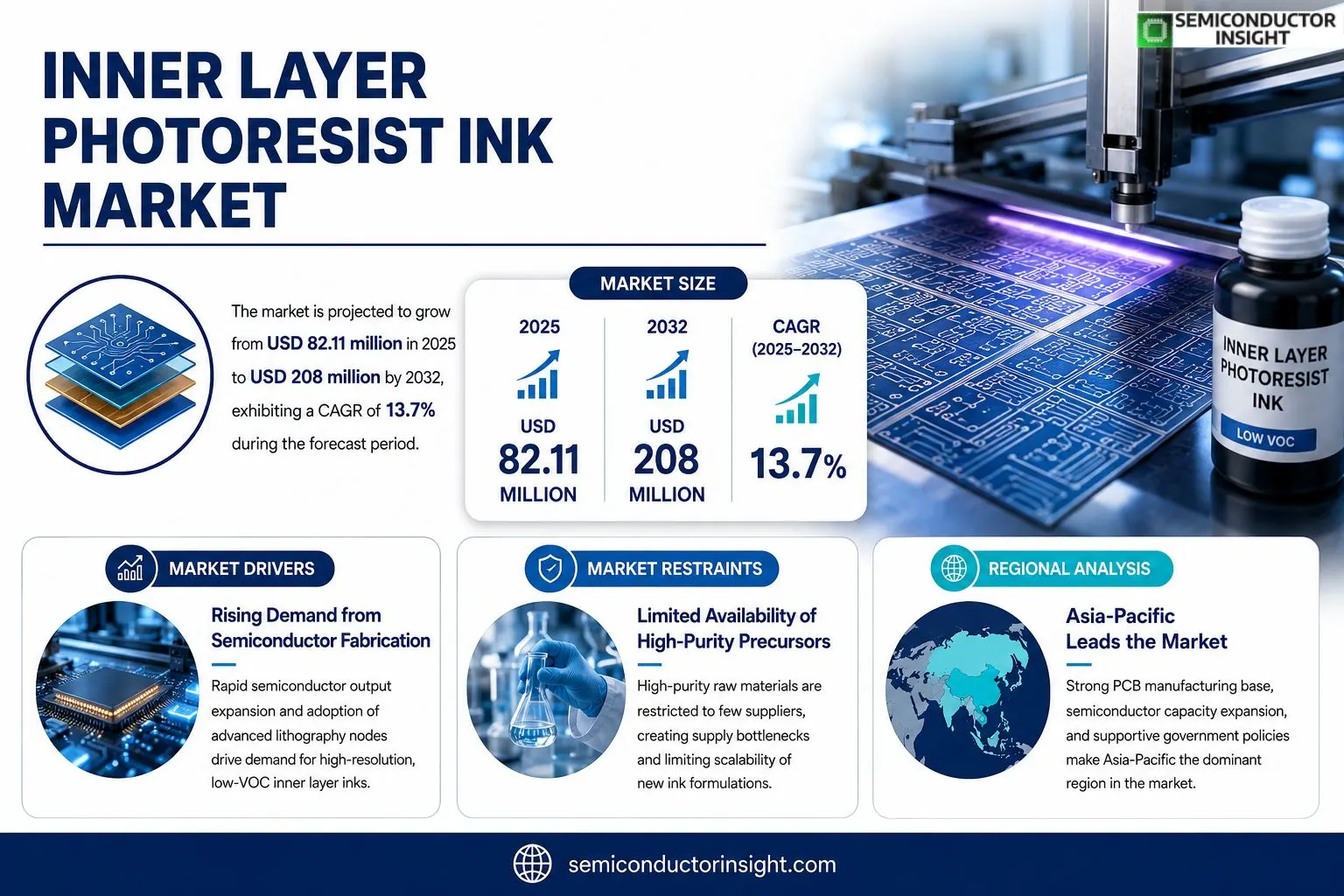
Inner Layer Photoresist Ink market size was valued at USD 82.11 million in 2025 and is forecasted to reach USD 208 million by 2032, reflecting a compound annual growth rate of approximately 13.7% throughout the forecast horizon.
Inner Layer Photoresist Ink is a photosensitive formulation employed to transfer inner‑layer circuit patterns during the fabrication of multilayer printed circuit boards. The material creates fine conductive traces on copper foil through exposure and development steps and serves as a core component of PCB photoresist systems. In 2025 production amounted to roughly 24 426 tons, with an average price near USD 3 681 per ton. Annual capacity stands at about 40 000 tons and industry gross margins range between 25% and 45%.The expansion of high‑density interconnect (HDI) and flexible circuit applications fuels demand because manufacturers require finer resolution, stronger adhesion, and enhanced chemical resistance. Environmental regulations encourage low‑VOC formulations, prompting suppliers toward greener chemistries. Policy initiatives such as “Made in China 2025” and dual‑carbon targets further stimulate domestic innovation, enabling several Chinese firms to replace imported products in key performance categories.
MARKET DRIVERS
Rising Demand from Semiconductor Fabrication
Inner Layer Photoresist Ink Market is feeling the impact of continuous capacity expansion among leading semiconductor fabs. As chip producers push output beyond 500 million wafers annually, they require inks that deliver finer line definition while tolerating higher exposure energies. Manufacturers are therefore opting for formulations that combine low viscosity with enhanced adhesion, a trend that fortifies demand for specialty suppliers.
Shift Toward Advanced Lithography Nodes
Adoption of extreme ultraviolet (EUV) lithography has forced fabs to reassess their inner‑layer coating strategies. EUV exposure necessitates resist chemistries capable of withstanding photon‑induced stress without compromising resolution. Suppliers that can deliver inks with tailored absorption spectra gain a competitive edge, prompting R&D investment across the sector.
➤ “The migration to sub‑45 nm processes is prompting manufacturers to prioritize high‑performance inner layer photoresist inks.”
Collectively, these forces translate into a steady upward trajectory for Inner Layer Photoresist Ink Market, encouraging vertical integration and partnership models that lock in supply for critical downstream processes.
MARKET CHALLENGES
Supply Chain Volatility
Recent disruptions in petrochemical feedstock availability have amplified cost uncertainty for photoresist producers. Price swings of up to 15 % over a quarter ripple through the ink supply chain, forcing fab managers to adjust procurement cycles and inventory buffers. Cost management becomes a pivotal concern as budgets tighten.
Other Challenges
Regulatory Scrutiny
Stringent chemical‑safety regulations in Europe and Asia require comprehensive documentation of resin constituents. Compliance testing adds lead time, and any failure to meet REACH or comparable standards can halt shipments, creating a bottleneck for firms lacking dedicated regulatory teams.
MARKET RESTRAINTS
Limited Availability of High‑Purity Precursors
The production of ultra‑high‑purity solvents and photo‑active compounds is confined to a handful of specialty chemical plants. Capacity constraints at these sites limit the scalability of new ink blends, curbing the ability of smaller formulators to meet rising fab specifications. Supply bottlenecks thus act as a structural ceiling on market expansion.
MARKET OPPORTUNITIES
Emerging Applications in Advanced Packaging
Beyond logic chips, the rise of fan‑out wafer‑level packaging (FOWLP) and heterogeneous integration opens fresh avenues for inner layer photoresist inks. These architectures demand resist layers that can endure multiple coating and de‑capping cycles while preserving pattern fidelity. Companies that engineer inks tailored for such processes stand to capture a growing share of a segment projected to double its volume within five years.
Inner Layer Photoresist Ink Market Trends
Shift Toward High‑Resolution, Low‑VOC Formulations
The industry’s momentum is now anchored in the need for finer circuit lines as multilayer printed circuit boards evolve toward greater density. Production of 24,426 tons in 2025 at an average price of $3,681 per ton reflects a market that already commands premium pricing for materials that can sustain sub‑10‑micron features. Anticipated demand from HDI and flexible circuit segments pushes manufacturers to invest in photoinitiators and resin systems that deliver both higher adhesion and reduced volatile organic compound emissions. In practice, the transition translates into a price premium of roughly 12 % over conventional inks, a margin that aligns with the 25 %‑45 % gross profit envelope observed across the sector.
Other Trends
Supply‑Chain Cost Pressures
Raw‑material expenses dominate the cost structure, accounting for 55 %‑70 % of total outlay, with resin and photosensitive components forming the bulk of that share. Manufacturing overheads (15 %‑25 %) and labor costs (10 %‑15 %) leave limited leeway for price competition, forcing firms to pursue formula optimization and yield‑boosting process control. The 40,000‑ton annual capacity cushion provides some resilience, yet any sustained increase in monomer prices would compress the gross margin band toward its lower threshold.
Technology‑Driven Consolidation
Technical barriers have risen as customers increasingly demand certification against the new “Wet Film Photoresist for PCB” standard. Companies that can demonstrate compliance through documented film‑thickness uniformity and chemical‑resistance data secure preferential access to high‑end OEM contracts. This dynamic encourages strategic acquisitions of niche resin developers and amplifies the market’s tilt from pure price competition to capability‑based differentiation. Domestic players in China have already leveraged policy incentives to replace imported formulations, widening the competitive field for locally sourced, low‑VOC products.
Policy and Standardization Momentum
Government initiatives such as the “Made in China 2025” plan and dual‑carbon emission targets have created a clear signal for greener ink chemistries. The push for low‑VOC, environmentally compliant formulations dovetails with the industry’s own profit motive, as reduced emissions cut energy consumption and simplify waste‑handling costs. Consequently, Inner Layer Photoresist Ink Market is reshaping its value chain: upstream suppliers are reformulating raw materials, while downstream PCB makers prioritize suppliers that can certify compliance, thereby reinforcing a virtuous cycle of innovation and market expansion.
COMPETITIVE LANDSCAPE
Key Industry Players
Competitive Overview of Inner Layer Photoresist Ink Market
The inner‑layer photoresist ink segment is dominated by a handful of firms that have built vertically integrated supply chains, from resin synthesis to final formulation. Shanghai Biren Technology, leveraging its proprietary azo‑based resin platform, captures roughly a quarter of shipments and sets pricing benchmarks for high‑resolution HDI boards. Its scale enables a gross margin near the top of the 25‑45 % range, compelling smaller suppliers to specialize in niche applications such as flexible circuit boards where adhesion and low‑VOC characteristics are paramount. The market structure therefore reflects a dual tier: a concentrated core that supplies the majority of volume to multinational PCB manufacturers, and a peripheral cluster of agile players that differentiate through customized chemistries or regional regulatory compliance.Beyond the leading tier, several companies have carved out defensible positions in specific geographies or product formats. Taiyo Holdings and Chang Chun Group dominate the Japanese and Taiwanese markets respectively, offering “ordinary‑type” inks with solid content above 50 % that meet strict environmental standards. Domestic Chinese firms such as Shenzhen RongDa Photosensitive Science & Technology and Wuxi Derbell Photo‑electronic Materials focus on low‑VOC formulations that align with the “dual carbon” policy, gaining traction among automotive electronics assemblers. European entrants like Merck KGaA and AGC Inc provide specialty additives that enhance adhesion on high‑speed copper foils, while U.S. players Dow and Fujifilm supply high‑purity solvents that support sub‑10 µm line widths for advanced semiconductor packaging. This diversified competitive set creates a landscape where technology leadership, regulatory alignment, and supply‑chain resilience are decisive factors for market share advancement.
List of Key Inner Layer Photoresist Ink Companies Profiled
- Shanghai Biren Technology
- Shenzhen RongDa Photosensitive Science & Technology
- Taiyo Holdings
- Chang Chun Group
- Wuxi Derbell Photo‑electronic Materials
- Guangdong SQ UV Curing Materials
- Jiangsu Kuangshun Photosensitivity New‑material Stock
- Guangzhou Jianke Electronic Materials
- Merck KGaA
- Dow
- Fujifilm
- AGC Inc.
- Hexion
- Nihon Dempa Kogyo
Segment Analysis:
| Segment Category | Sub-Segments | Key Insights |
| By Type |
|
Ordinary Type remains the dominant choice because it delivers reliable adhesion and consistent resolution for conventional PCB manufacturing. – Manufacturers value its proven processing window and compatibility with existing equipment. – Ongoing refinements target lower VOC emissions while preserving performance, aligning with green‑manufacturing policies. – The segment benefits from broad supplier base and incremental innovations that reinforce its market preference. |
| By Application |
|
HDI Board is emerging as the leading application due to the industry shift toward higher density interconnects and finer line/space requirements. – Ink formulations are being optimized for superior resolution and chemical resistance, essential for micro‑via creation. – Customers prioritize inks that support low‑temperature processing to integrate with advanced substrate materials. – The segment is driven by demand from smartphones, automotive infotainment, and high‑performance computing where performance margins are tight. |
| By End User |
|
Consumer Electronics drives most of the ink demand because of rapid product cycles and the need for highly reliable PCB stacks. – The segment values inks that enable quick exposure/development cycles, supporting high‑volume production. – Sustainability expectations push suppliers toward low‑VOC and recyclable formulations. – Integration with emerging form‑factor devices such as wearables intensifies focus on thin‑film flexibility and durability. |
| By Product Type |
|
Colorless dominates as the primary visual preference for process engineers seeking minimal visual interference during exposure. – Its transparency aids in accurate alignment and defect detection. – R&D efforts focus on enhancing photoinitiator efficiency to maintain performance while reducing coloration. – The blue variant finds niche use where contrast is needed for manual inspection steps. |
| By Solid Content |
|
>50% Solid Content is gaining attention as manufacturers pursue higher print density and reduced solvent handling. – The higher solid loading improves film uniformity and reduces post‑exposure bake times. – Process adaptations focus on viscosity management to ensure smooth coating. – Environmental compliance programs favor reduced solvent emissions, reinforcing the move toward higher solid content formulations. |
Regional Analysis: Inner Layer Photoresist Ink Market
Asia-Pacific
Taiwan’s integrated circuit valleys host a concentration of wafer fabs that continuously push process linewidths lower, compelling ink suppliers to tailor formulations for tighter feature control and reduced defectivity.
Regional logistics networks now prioritize just‑in‑time delivery of high‑purity chemicals, a shift that diminishes inventory holding costs and aligns closely with the fast‑paced development cycles of Inner Layer Photoresist Ink Market.
Universities in South Korea and Singapore are feeding the sector with graduates specialized in polymer chemistry and nanofabrication, ensuring a steady pipeline of expertise for complex ink engineering tasks.
Collaborative labs near major foundries are experimenting with environmentally benign solvents, positioning the region at the forefront of sustainability trends within Inner Layer Photoresist Ink Market.
North America
The United States maintains a strategic foothold through its advanced research institutions and a robust ecosystem of specialty chemical firms. While domestic fabs have scaled back in recent years, the emphasis on developing next‑generation lithography tools sustains demand for high‑performance inks. Partnerships between academia and industry accelerate proof‑of‑concept trials, and a regulatory climate that encourages innovation grants U.S. players a differentiation edge, particularly in niche applications such as quantum‑ready photolithography.
Europe
European semiconductor clusters, notably in Germany and the Netherlands, prioritize precision engineering and low‑defect processes. The region’s strong orientation toward circular‑economy principles drives ink manufacturers to explore recyclable carrier systems and reduced‑waste chemistries. Collaborative frameworks across the EU facilitate shared testing facilities, enabling a collective response to the evolving specifications of Inner Layer Photoresist Ink Market without sacrificing individual country competitiveness.
South America
Brazil and Chile are emerging as supportive markets, largely driven by government initiatives aimed at diversifying the electronics supply chain away from traditional hubs. Although production volumes remain modest, local demand for high‑quality photoresist formulations is rising as regional research labs pursue advanced packaging technologies. This nascent activity creates opportunities for niche suppliers willing to offer customized support and technical consultancy.
Middle East & Africa
In the Middle East, the United Arab Emirates has launched semiconductor‑focused investment zones that attract equipment vendors and specialty chemical providers. Africa’s contribution is still limited, yet nations such as South Africa are experimenting with localized pilot lines, primarily for educational and prototyping purposes. These early‑stage endeavors suggest a longer horizon, but they lay groundwork for future participation in Inner Layer Photoresist Ink Market as regional expertise matures.
Report Scope
This market research report provides a comprehensive analysis of the Inner Layer Photoresist Ink Market , covering the forecast period 2026–2034. It offers detailed insights into market dynamics, technological advancements, competitive landscape, and key trends shaping the industry.
Key focus areas of the report include:
- Market Overview: The report begins with an overview outlining its current market scenario, key growth indicators, and industry transformation drivers. It discusses macroeconomic factors, demand–supply balance, regulatory landscape, and the strategic role of semiconductors in powering advancements across industries such as automotive, telecommunications, consumer electronics, and industrial automation.
- Market Size & Forecast: Historical data and future projections for revenue, unit shipments, and market value across major regions and segments.
- Segmentation Analysis: Detailed breakdown by product type, technology, application, and end-user industry to identify high-growth segments and investment opportunities.
- Regional Insights: Insights into market performance across North America, Europe, Asia-Pacific, Latin America, and the Middle East & Africa, including country-level analysis where relevant.
- Competitive Landscape: Profiles of leading market participants, including their product offerings, R&D focus, manufacturing capacity, pricing strategies, and recent developments such as mergers, acquisitions, and partnerships.
- Technology Trends & Innovation: Assessment of emerging technologies, integration of AI/IoT, semiconductor design trends, fabrication techniques, and evolving industry standards.
- Market Drivers & Restraints: Evaluation of factors driving market growth along with challenges, supply chain constraints, regulatory issues, and market-entry barriers.
- Stakeholder Insights: Insights for component suppliers, OEMs, system integrators, investors, and policymakers regarding the evolving ecosystem and strategic opportunities.
Primary and secondary research methods are employed, including interviews with industry experts, data from verified sources, and real-time market intelligence to ensure the accuracy and reliability of the insights presented.
FREQUENTLY ASKED QUESTIONS:
What is the current market size of Inner Layer Photoresist Ink Market?
-> Inner Layer Photoresist Ink Market was valued at USD 82.11 million in 2025 and is expected to reach USD 208 million by 2032, growing at a CAGR of 13.7% during the forecast period.
Which key companies operate in Inner Layer Photoresist Ink Market?
-> Key players include Shanghai Biren Technology, Shenzhen RongDa Photosensitive Science & Technology, Taiyo Holdings, Chang Chun Group, Wuxi Derbell Photo‑electronic Materials, Guangdong SQ UV Curing Materials, Jiangsu Kuangshun Photosensitivity New‑material Stock, Guangzhou Jianke Electronic Materials.
What are the key growth drivers?
-> Key growth drivers include the shift toward high‑density, multi‑layer PCBs, stricter environmental regulations encouraging low‑VOC and green formulations, and strong policy support such as Made in China 2025 and dual‑carbon initiatives.
Which region dominates the market?
-> Asia dominates Inner Layer Photoresist Ink Market, driven by large PCB manufacturing bases in China, Japan, and South Korea.
What are the emerging trends?
-> Emerging trends include development of low‑VOC and harmless ink formulations, increasing technical barriers favoring high‑end certified products, and the establishment of standardized testing and quality benchmarks for wet‑film photoresist.

Get Sample Report PDF for Exclusive Insights
Report Sample Includes
- Table of Contents
- List of Tables & Figures
- Charts, Research Methodology, and more...
 Download Sample Report PDF