
Hybrid Bonding (Direct Cu-Cu) Equipment Market Insights
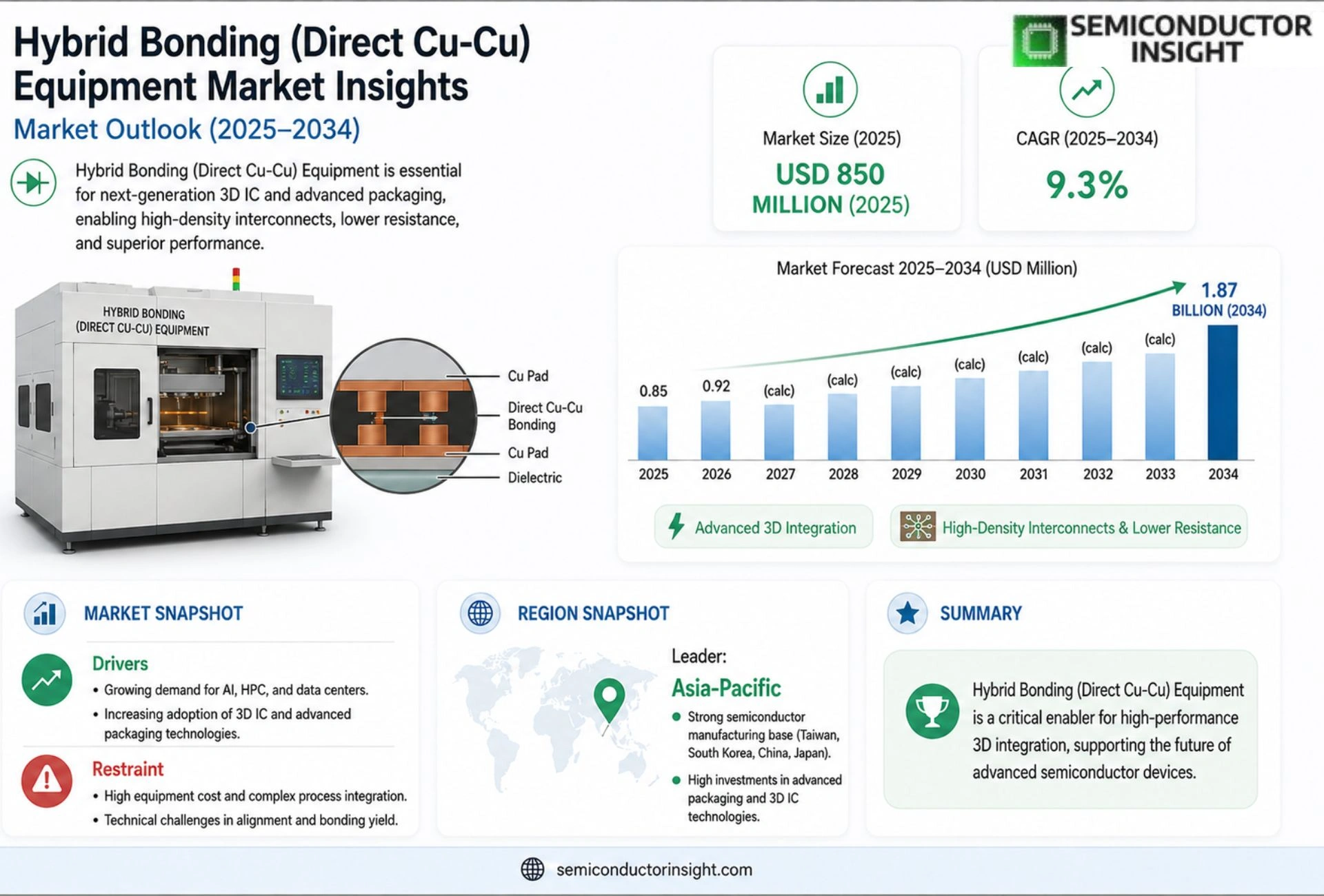
Global Hybrid Bonding (Direct Cu-Cu) Equipment market size was valued at USD 850 million in 2025. The market is projected to grow from USD 920 million in 2026 to USD 1.87 billion by 2034, exhibiting a CAGR of 9.3% during the forecast period.
Hybrid bonding (Direct Cu-Cu) equipment refers to advanced semiconductor manufacturing tools designed for direct copper-to-copper bonding, enabling high-density interconnections with superior electrical, thermal, and mechanical performance. This technology eliminates traditional solder-based connections, reducing pitch sizes below 10 micrometers while enhancing reliability and signal integrity,critical for next-generation applications such as 3D IC packaging, heterogeneous integration, and high-bandwidth memory (HBM). The process involves precision surface activation, alignment, and thermocompression bonding under controlled environments to achieve atomic-level adhesion between copper pads.
The rapid adoption of hybrid bonding is driven by escalating demand for miniaturization, higher I/O density, and improved power efficiency in consumer electronics, automotive sensors, and AI accelerators. Leading foundries and OSAT providers are increasingly integrating this technology into their production lines; for instance, TSMC’s SoIC (System on Integrated Chips) platform leverages hybrid bonding for chiplet-based architectures. Furthermore, industry collaborations,such as the partnership between Applied Materials and Besi announced in March 2024,to develop scalable hybrid bonding solutions underscore its strategic importance in addressing Moore’s Law limitations.
MARKET DRIVERS
Need for Increased Bandwidth in Semiconductor Packaging
The demand for ever-increasing data bandwidth in high-performance computing and networking applications is a primary catalyst for Hybrid Bonding (Direct Cu-Cu) Equipment Market. As traditional interconnection methods reach physical limits, manufacturers require solutions that support high-density wiring without sacrificing signal integrity. Hybrid bonding facilitates two-tier copper connections that significantly surpass the performance of through-silicon vias (TSVs) and redistribution layers, driving adoption across cutting-edge logic and memory technologies.
Proliferation of 3D Integrated Circuits and Heterogeneous Integration
The rapid shift towards 3D IC designs is fueling growth in this sector. By enabling direct bonding between silicon dies within the same third dimension, companies can achieve reduced path lengths and lower parasitic capacitance. This technical advantage is critical for reducing power consumption and improving thermal management in complex semiconductor systems.
➤ Market analysts project that hybrid bonding adoption will see a CAGR of over 15% through 2030.
This integration capability supports the growing trend of heterogeneous integration, where disparate components like sensors, logic, and memory are co-packaged to create more efficient system-level solutions.
MARKET CHALLENGES
High Capital Expenditure for Specialized Machinery
Implementing hybrid bonding requires significant upfront investment in specialized equipment capable of atomic-level precision. The cost of wafer-to-wafer and chip-to-wafer bonding machinery poses a barrier to entry for smaller foundries and OEMs, potentially restricting market growth to well-capitalized industry leaders.
Other Challenges
Process Complexity and Control
Maintaining atomic-level flatness and surface cleanliness during the bonding process is difficult. Even minute particulate matter or surface defects can cause catastrophic failure in the resulting 3D stack.
Yield Management Issues
Ensuring repeatable high yields in multi-layer 3D structures remains a sophisticated engineering obstacle. The delicate thermal and mechanical stresses involved often complicate process optimization compared to standard flip-chip bonding.
MARKET RESTRAINTS
Stringent Reliability Requirements for Consumer Electronics
The consumer electronics sector demands components that withstand rapid temperature fluctuations and thermal cycling. Current validation data suggests that long-term stability of direct copper-to-copper interfaces in high-volume consumer goods is still under rigorous testing, creating hesitation for some mass-market applications.
MARKET OPPORTUNITIES
Advancements in 5G and AI Infrastructure
The explosive growth of Artificial Intelligence and 5G infrastructure drives the need for advanced packaging solutions that can handle massive data throughput. The semiconductor equipment market targeting these high-performance segments presents lucrative opportunities for vendors specializing in hybrid bonding equipment capable of meeting these industrial-scale demands.
Trends
Primary Trend Heading Here
Hybrid Bonding (Direct Cu-Cu) Equipment Market is experiencing significant growth, driven by the increasing need for advanced semiconductor packaging solutions. The ability to achieve high-density interconnections with direct copper-to-copper bonding is revolutionizing the landscape of next-generation electronic devices. This technology addresses the limitations of traditional solder-based bonding, enabling smaller form factors and improved performance. The market is projected for substantial expansion in the coming years, reflecting the growing adoption of this technology across various industries.
Other Trends
Rising Demand for Miniaturization
The relentless pursuit of miniaturization in consumer electronics and other applications is a key driver for Hybrid Bonding (Direct Cu-Cu) Equipment Market. The technology facilitates the creation of smaller, more powerful devices by enabling the integration of multiple chiplets into a single package. This trend is particularly pronounced in areas like smartphones, wearables, and Internet of Things (IoT) devices, where space constraints are paramount. The utilization of hybrid bonding allows for significantly reduced pitch sizes, far below 10 micrometers, which is crucial for achieving these compact designs.
Heterogeneous Integration Advancements
Heterogeneous integration, the process of combining different types of chips and components within a single package, is gaining momentum. Hybrid Bonding (Direct Cu-Cu) Equipment plays a crucial role in this trend by providing a reliable and high-performance method for interconnecting diverse semiconductor materials. This capability allows for the creation of customized solutions tailored to specific application requirements, leading to enhanced functionality and efficiency. The inherent advantages of direct copper-to-copper bonding contribute significantly to the reliability and performance of these heterogeneous systems.
Increased Adoption in AI and High-Performance Computing
The burgeoning field of artificial intelligence (AI) and high-performance computing (HPC) is fueling demand for advanced packaging technologies. Hybrid Bonding (Direct Cu-Cu) Equipment is well-suited for creating 3D ICs and packaging solutions required for AI accelerators and HPC systems. The technology’s ability to support high bandwidth and low latency is critical for these demanding applications. As AI models become increasingly complex and data processing requirements escalate, the need for advanced interconnect technologies like hybrid bonding will continue to grow.
Strategic Collaborations and Technological Innovations
Hybrid Bonding (Direct Cu-Cu) Equipment Market is witnessing increased strategic collaborations between leading semiconductor equipment suppliers and foundries. These partnerships are focused on developing scalable and cost-effective hybrid bonding solutions. For example, collaborations between Applied Materials and Besi highlight the industry’s commitment to overcoming the technical challenges associated with this technology. Ongoing research and development efforts are continuously improving the precision, reliability, and throughput of hybrid bonding processes, further solidifying its position in the semiconductor manufacturing ecosystem.
COMPETITIVE LANDSCAPE
Key Industry Players
Hybrid Bonding (Direct Cu-Cu) Equipment Market
The global Hybrid Bonding (Direct Cu-Cu) Equipment market is experiencing robust growth, projected to reach USD 1.87 billion by 2034 with a CAGR of 9.3%. This growth is fueled by the increasing demand for miniaturization and higher I/O density in various applications, including 3D IC packaging and AI accelerators. Key players in this competitive landscape are focused on developing advanced tools to facilitate high-density interconnections using direct copper-to-copper bonding technology, a significant advancement over traditional solder-based methods.
Several companies are actively involved in providing equipment and solutions for hybrid bonding. These include established semiconductor equipment manufacturers expanding their portfolios and specialized companies focusing specifically on this emerging technology. Strategic collaborations and technological advancements are further driving innovation and market expansion within the Hybrid Bonding (Direct Cu-Cu) Equipment sector. The integration of this technology by leading foundries underscores its crucial role in future semiconductor innovation.
List of Key Hybrid Bonding Companies Profiled
- Applied Materials
- Applied Materials
- Besi GmbH
- Besi
- ASML Holding N.V.
- ASML
- Tokyo Electron Limited
- Tokyo Electron
- Lam Research Corporation
- Lam Research
- KLA Corporation
- KLA
- Advantest Corporation
- Advantest
- SCREEN Holdings Co., Ltd.
- SCREEN
Segment Analysis:
| Segment Category | Sub-Segments | Key Insights |
| By Type |
|
Direct Cu-Cu Bonding Systems are the core equipment used for establishing high-density interconnections between copper components. These systems are characterized by their precision and control in surface activation, alignment, and bonding processes, addressing the growing need for miniaturization in semiconductor devices. Hybrid Bonding Stencils enable precise placement and alignment of components during the bonding process, contributing to improved yield and reliability. Bonding Equipment Accessories encompass a range of supporting components that enhance the functionality and efficiency of the primary bonding systems. |
| By Application |
|
3D IC Packaging represents a significant driver for hybrid bonding technology, enabling the vertical stacking of multiple chiplets to enhance performance and functionality. Heterogeneous Integration leverages hybrid bonding to combine diverse chiplets with varying functionalities onto a single package, optimizing system performance and efficiency. High-Bandwidth Memory (HBM) heavily relies on hybrid bonding to achieve the required high data transfer rates and dense interconnects for demanding applications. |
| By End User |
|
Semiconductor Foundries are key adopters of hybrid bonding to offer advanced packaging solutions for their customers. Original Design Manufacturers (ODMs) utilize hybrid bonding to create customized electronic products with enhanced performance and miniaturization. Original Equipment Manufacturers (OEMs) are increasingly incorporating hybrid bonding into their products to meet the demands for higher performance and integration capabilities. |
| By Material |
|
Copper is the primary material used in direct Cu-Cu bonding due to its excellent electrical and thermal conductivity. Copper Alloys are sometimes employed to enhance specific properties like strength or solderability in certain bonding applications. |
| By Process |
|
Thermocompression Bonding is the core process involving controlled pressure and temperature to achieve the Cu-Cu bond. Surface Activation techniques are crucial for preparing the copper surfaces to ensure strong and reliable bonding. |
Regional Analysis:
Ongoing research and development efforts are leading to more efficient and versatile Hybrid Bonding equipment. Innovations in bonding processes, materials, and process control are crucial for addressing the increasing complexity of modern integrated circuits.
Strategic partnerships between equipment manufacturers, semiconductor foundries, and research institutions are fostering innovation and accelerating the adoption of Hybrid Bonding technologies. These collaborations are essential for developing tailored solutions and addressing specific industry challenges.
The increasing demand for high-performance, power-efficient electronic devices, coupled with the need for advanced packaging solutions, is a primary driver for the Hybrid Bonding equipment market in North America.
The North American market features a mix of established and emerging players, each offering specialized Hybrid Bonding equipment and services. Competition is intense, with companies focusing on product differentiation and customer-centric solutions.
Europe
Europe presents a mature and sophisticated market for Hybrid Bonding (Direct Cu-Cu) Equipment. Driven by strong automotive, industrial, and aerospace sectors, the demand for advanced packaging solutions is evident. European players are focusing on developing high-reliability and high-performance equipment catering to these demanding industries. Regulatory compliance and a strong emphasis on sustainable manufacturing practices are key considerations in this region. The adoption rate of Hybrid Bonding is steadily increasing, particularly in applications requiring robust thermal management and compact form factors. Hybrid Bonding (Direct Cu-Cu) Equipment Market in Europe is expected to witness steady growth.
Asia-Pacific
Asia-Pacific is anticipated to be the fastest-growing market for Hybrid Bonding (Direct Cu-Cu) Equipment in the coming years. Fueled by the rapid expansion of the semiconductor industry in countries like China, Taiwan, and South Korea, the demand for advanced packaging technologies is soaring. The region is witnessing significant investments in R&D and manufacturing capabilities, creating a fertile ground for the adoption of Hybrid Bonding. Government support for the semiconductor sector and the increasing focus on domestic chip production are further accelerating market growth. Hybrid Bonding (Direct Cu-Cu) Equipment Market is poised for significant expansion.
South America
South America represents an emerging market for Hybrid Bonding (Direct Cu-Cu) Equipment. While currently smaller in size compared to other regions, the market is expected to grow at a healthy pace driven by the expansion of electronics manufacturing and the increasing demand for sophisticated electronic devices. The automotive and telecommunications industries are key drivers of this growth. Hybrid Bonding (Direct Cu-Cu) Equipment Market is in its early stages of development.
Middle East & Africa
The Middle East and Africa are nascent markets for Hybrid Bonding (Direct Cu-Cu) Equipment. The electronics industry in these regions is still developing, but with increasing investments in infrastructure and technology, the demand for advanced packaging solutions is expected to rise. The growth of the telecommunications and consumer electronics sectors will be key drivers for market expansion. Hybrid Bonding (Direct Cu-Cu) Equipment Market has significant growth potential.
Report Scope
This market research report provides a comprehensive analysis of the Hybrid Bonding (Direct Cu-Cu) Equipment Market , covering the forecast period 2026–2034. It offers detailed insights into market dynamics, technological advancements, competitive landscape, and key trends shaping the industry.
Key focus areas of the report include:
- Market Overview: The report begins with an overview outlining its current market scenario, key growth indicators, and industry transformation drivers. It discusses macroeconomic factors, demand–supply balance, regulatory landscape, and the strategic role of semiconductors in powering advancements across industries such as automotive, telecommunications, consumer electronics, and industrial automation.
- Market Size & Forecast: Historical data and future projections for revenue, unit shipments, and market value across major regions and segments.
- Segmentation Analysis: Detailed breakdown by product type, technology, application, and end-user industry to identify high‑growth segments and investment opportunities.
- Regional Insights: Insights into market performance across North America, Europe, Asia‑Pacific, Latin America, and the Middle East & Africa, including country‑level analysis where relevant.
- Competitive Landscape: Profiles of leading market participants, including their product offerings, R&D focus, manufacturing capacity, pricing strategies, and recent developments such as mergers, acquisitions, and partnerships.
- Technology Trends & Innovation: Assessment of emerging technologies, integration of AI/IoT, semiconductor design trends, fabrication techniques, and evolving industry standards.
- Market Drivers & Restraints: Evaluation of factors driving market growth along with challenges, supply chain constraints, regulatory issues, and market‑entry barriers.
- Stakeholder Insights: Insights for component suppliers, OEMs, system integrators, investors, and policymakers regarding the evolving ecosystem and strategic opportunities.
Primary and secondary research methods are employed, including interviews with industry experts, data from verified sources, and real‑time market intelligence to ensure the accuracy and reliability of the insights presented.
FREQUENTLY ASKED QUESTIONS:
What is the current market size of Hybrid Bonding (Direct Cu-Cu) Equipment Market?
-> Global Hybrid Bonding (Direct Cu-Cu) Equipment Market was valued at USD 850 million in 2025 and is expected to reach USD 1.87 billion by 2034, reflecting a CAGR of 9.3% during the forecast period.
Which key companies operate Hybrid Bonding (Direct Cu-Cu) Equipment Market?
-> Key players include TSMC, Applied Materials, Besi and other leading foundries and OSAT providers.
What are the key growth drivers?
-> Key growth drivers include miniaturization, higher I/O density, improved power efficiency, and rising demand in consumer electronics, automotive sensors, and AI accelerators.
Which region dominates the market?
-> The market shows strong activity across major semiconductor hubs, particularly in Asia‑Pacific, North America and Europe, with no single region overwhelmingly dominant.
What are the emerging trends?
-> Emerging trends include chiplet‑based architectures, 3D‑IC packaging, heterogeneous integration, and scalable hybrid bonding solutions driven by collaborations such as Applied Materials & Besi.

Get Sample Report PDF for Exclusive Insights
Report Sample Includes
- Table of Contents
- List of Tables & Figures
- Charts, Research Methodology, and more...
 Download Sample Report PDF


