Key Statistics
Key Takeaways
- FOUP is the leading product type because automated 300 mm fabs require repeated in-fab wafer movement between stockers, process tools and metrology equipment under tightly controlled microenvironment conditions.
- 300 mm Wafer is the dominant application because leading logic, DRAM and NAND manufacturing is centered on 300 mm lines. SEMI reported that 15 of the 18 new fab construction projects expected to start in 2025 were 300 mm facilities.
- Asia Pacific is the largest market, reflecting the concentration of wafer manufacturing in Taiwan, South Korea, Japan and China and the dense regional supply base for carriers, automation and semiconductor materials.
- Advanced carrier variants are expanding the value pool. Thin, bonded, warped and heavy wafers require altered support geometry, purge options, electrostatic control and microenvironment materials while preserving compatibility with automated fab equipment.
- Fab localization supports regional growth outside Asia. TSMC’s Arizona plan exceeds USD 65 billion across three greenfield fabs, while the EU Chips Act is expected to support more than EUR 100 billion of policy-driven public and private investment through 2030.
Semiconductor FOUP and FOSB Market Overview
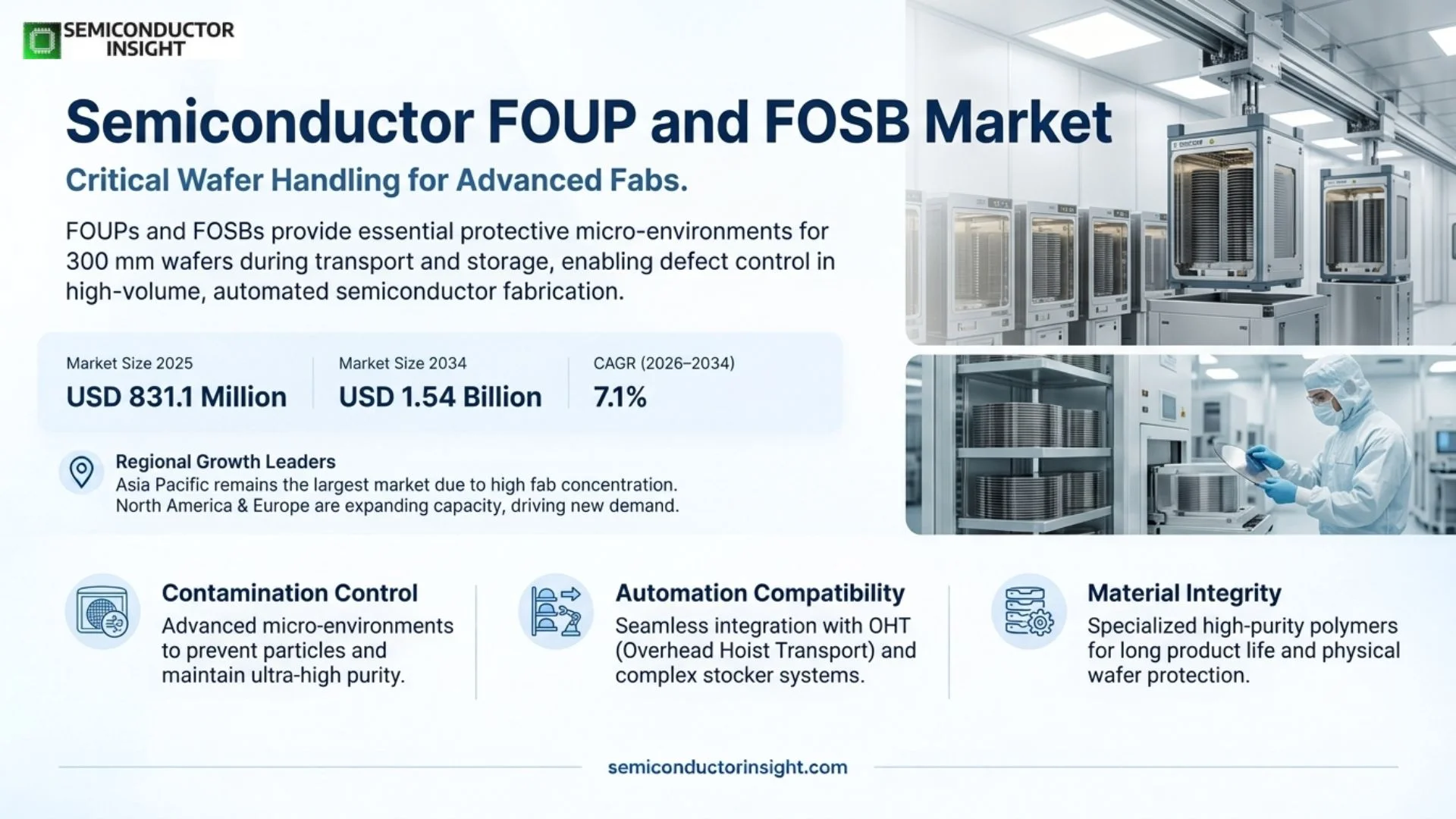
Semiconductor FOUP and FOSB Market was valued at USD 831.1 million in 2025 and is projected to reach USD 1.54 billion by 2034, expanding at a 7.1% CAGR during 2026–2034. Asia Pacific is the largest regional market because the highest concentration of 300 mm wafer fabrication and memory capacity is located in Taiwan, South Korea, Japan and China, while North America and Europe are adding new fabs that expand the need for clean, automation-compatible wafer carriers.
Front Opening Unified Pods (FOUPs) and Front Opening Shipping Boxes (FOSBs) are specialized wafer carriers used to protect semiconductor wafers during in-fab handling, storage and transport. FOUPs interface with automated material handling systems and process tools, while FOSBs are optimized for secure wafer shipment between manufacturing, foundry, OSAT and customer locations. Both products protect against particles, mechanical damage and environmental exposure that can affect wafer yield.
The market is closely tied to 300 mm manufacturing because larger wafers carry high economic value and move through hundreds of process steps before completion. Entegris describes modern 300 mm FOUPs as controlling not only particles but also volatile organic compounds, oxygen and relative humidity while integrating with fab automation. SEMI projected global 300 mm fab-equipment spending of USD 133 billion in 2026, rising to USD 151 billion in 2027, creating a strong installed-base expansion signal for wafer carriers.
Carrier requirements are also evolving with advanced packaging and wafer thinning. Thin, thick, bonded and warped wafers can require different slot spacing, support geometry and materials. Entegris offers 13-capacity thin-wafer FOUPs as well as carriers for thick and warped 300 mm wafers, demonstrating how the market is shifting from a single standardized carrier toward application-specific fleets that preserve automation compatibility while controlling wafer sag, contamination and electrostatic risk.
Segment Analysis: By Type
By type, the source-defined market includes FOUP and FOSB. FOUPs represent the larger value pool because they are integrated into automated material handling and process-tool interfaces throughout the fab, while FOSBs are essential for protecting wafers during external shipment and inter-site transfer.
| Type | Technical / functional role | Market position and purchasing logic |
|---|---|---|
| FOUP | A front-opening carrier designed for automated 300 mm wafer handling inside semiconductor fabs. FOUP doors, kinematic interfaces, wafer supports, identification features and optional purge functions are engineered for reliable interaction with load ports, stockers and automated material handling systems. | Leading type. Each active 300 mm fab requires a fleet of carriers sized to wafer starts, work-in-process buffers and route complexity. Demand is recurring because carriers wear, contamination performance must be maintained and new process flows can require different materials, purge options or wafer-support configurations. |
| FOSB | A protective front-opening shipping box used to transport wafers between manufacturing sites, foundries, OSATs and customers. The design prioritizes mechanical protection, cleanliness, secure wafer spacing and packaging compatibility during logistics rather than repeated automated process-tool interfacing. | FOSB demand follows inter-company wafer shipments, foundry-customer transfers and multi-site manufacturing. Commercial requirements emphasize contamination control, durability, validated packaging and return-cycle economics, with regional semiconductor supply-chain restructuring creating new shipment lanes and fleet requirements. |
Why carrier microenvironment control is becoming more valuable
As device geometries shrink and wafer value rises, a carrier is increasingly treated as a controlled process microenvironment rather than passive packaging. Particle generation, humidity, oxygen, outgassing, electrostatic discharge and wafer-support contact can all affect downstream yield. Suppliers therefore compete through high-purity polymers, barrier materials, purge capability, validated door systems, identification options and long mechanical life in addition to basic dimensional compliance.
Segment Analysis: By Application
By application, the source-defined market comprises 300 mm Wafer and 200 mm Wafer. The 300 mm segment is the principal growth engine because leading logic and memory fabs use 300 mm substrates and rely heavily on automated carrier handling, while 200 mm demand remains important in mature analog, power, MEMS and specialty semiconductor manufacturing.
| Application | Demand characteristics |
|---|---|
| 300 mm Wafer | Largest application. Modern leading-edge logic and memory fabs are designed around automated 300 mm handling, making FOUPs integral to fab logistics. SEMI expected 15 of the 18 new fab construction projects starting in 2025 to be 300 mm facilities, and projected 300 mm equipment spending of USD 133 billion in 2026. |
| 200 mm Wafer | 200 mm manufacturing remains important for analog, power, MEMS, automotive and other mature-node products. Carrier requirements are less standardized around FOUP architecture than leading 300 mm lines, but fabs still require clean, durable wafer transport and shipping solutions. Demand is supported by long-lived specialty fabs and capacity additions where 200 mm economics remain attractive. |
Regional Analysis
Asia Pacific is the largest Semiconductor FOUP and FOSB market because it hosts the densest concentration of 300 mm logic and memory manufacturing. North America is entering a major localization cycle, Europe is expanding strategic semiconductor capacity, and South America and the Middle East & Africa remain smaller markets tied to specialty manufacturing, research and imported wafer handling systems.
How does the new-fab pipeline translate into carrier demand?
FOUP demand scales with the installed 300 mm fab base, wafer starts, work-in-process inventory and the number of process moves, while FOSB demand follows external wafer shipments and inter-site logistics. SEMI expected 18 new fab construction projects to start in 2025, including 15 300 mm facilities. Eleven of the 18 projects were located in Japan, China, Taiwan, Korea or Southeast Asia, while four were in the Americas and three across Europe & Middle East. This is a direct indicator of where new carrier fleets will be required as fabs move toward operation.
| Region | Position | Growth outlook | Demand profile | Evidence-led market logic |
|---|---|---|---|---|
| Asia Pacific | Largest | Strong | High-volume 300 mm manufacturing | Japan, China, Taiwan, Korea and Southeast Asia represented 11 of the 18 new fab starts SEMI expected in 2025, reinforcing the region’s carrier fleet and wafer-shipping demand. |
| North America | Major growth market | Strong | Localization and leading-edge fabs | The source page valued North America at USD 188.81 million in 2023. TSMC Arizona’s planned investment exceeds USD 65 billion across three leading-edge fabs, supporting new FOUP fleet demand. |
| Europe | Strategic market | Moderate to strong | Specialty and policy-led expansion | The EU Chips Act should result in more than EUR 43 billion of public investment and more than EUR 100 billion of policy-driven public and private investment through 2030. |
| South America | Smaller base | Selective | Import and specialty manufacturing | Demand is tied to smaller semiconductor, electronics and research operations and is commonly served through global carrier vendors rather than local large-scale production. |
| Middle East & Africa | Emerging | Project-led | New ecosystem development | Regional technology investment creates selective opportunities, but carrier demand remains concentrated in research, specialty semiconductor operations and early-stage fab projects. |
Competitive Landscape
Competition is concentrated among specialist wafer-handling suppliers that must combine high-purity materials, dimensional precision, automation compatibility and contamination control. Qualification is demanding because a carrier interacts physically with wafers, load ports, stockers and automated transport systems across thousands of handling cycles. Once a design is qualified, fleet replacement and expansion create recurring revenue but customers expect long product life and stable change control.
Entegris is a major global supplier with a broad 300 mm FOUP platform covering standard, thin, thick, warped and heavy-wafer applications. Shin-Etsu Polymer and Miraial bring established Japanese materials and carrier expertise, while Gudeng Precision, Chuang King Enterprise and 3S Korea compete from Asian semiconductor supply clusters. Dainichi Shoji also participates in the source-defined competitive landscape.
Differentiation is shifting toward microenvironment performance. Modern FOUPs use optimized polymer systems, purge features, electrostatic protection, RFID and refined wafer-support geometry to reduce particle, humidity, oxygen and volatile-organic exposure. Thin and warped wafers introduce additional mechanical requirements, so carrier design is becoming more application-specific even while external automation interfaces remain standardized.
FOSB competition places greater weight on shipping durability, wafer restraint, cleanliness, return-cycle economics and packaging validation. Customers may use multiple carrier types across a supply chain: FOUPs for automated in-fab movement and FOSBs for external shipment, creating opportunities for vendors that can provide a consistent family of wafer-handling products and lifecycle services.
| Competitive tier | Representative companies | How they compete |
|---|---|---|
| Global platform leader | Entegris | Competes through a broad 300 mm FOUP portfolio, high-purity materials, microenvironment control, purge options, RFID and application-specific designs for thin, thick, warped and heavy wafers. |
| Established Japanese suppliers | Shin-Etsu Polymer; Miraial; Dainichi Shoji | Leverage close relationships with Japanese and Asian fabs, materials know-how, precision manufacturing and long semiconductor qualification experience. |
| Asian growth specialists | Chuang King Enterprise; Gudeng Precision; 3S Korea | Compete through proximity to Taiwan and South Korean semiconductor clusters, localized engineering support and growing product portfolios for high-volume wafer handling and shipping. |
Key Participants
Production Capacity Analysis
Production capacity depends on clean polymer molding, precision assembly, door and latch manufacturing, wafer-support geometry, filter or purge components, identification systems and contamination-controlled inspection. Effective capacity is constrained by semiconductor qualification and automation compatibility as much as molding throughput, because small dimensional or material changes can affect wafer access, particle generation or load-port interaction across an installed carrier fleet.
FOUP shells and doors use high-purity engineered polymers selected for mechanical stability, low contamination and electrostatic behavior. Entegris documents ultrapure polycarbonate and carbon-filled barrier materials in its A300 platforms. Tooling, molding conditions and cleanliness must remain tightly controlled because surface particles, outgassing or dimensional drift can become yield risks in advanced fabs.
Assembly adds precision wafer supports, door mechanisms, seals, filters, purge ports, handles and identification options such as RFID. Standard 300 mm FOUPs can hold 25 or 26 wafers, while specialized thin-wafer designs may use 13 positions with larger spacing to reduce sag and give automation more clearance. These variants expand product complexity and require dedicated qualification rather than simple commodity SKU expansion.
Lifecycle capacity matters after the initial sale. Fabs require cleaning, inspection, replacement parts and fleet management to keep carriers within contamination and mechanical specifications. Suppliers with regional service capability can reduce total ownership cost by extending carrier life and ensuring fast replacement of damaged doors, seals, filters and other components without disrupting fab material flow.
Market Dynamics
The market benefits from a sustained 300 mm fab investment cycle, recovering silicon wafer shipments and the growing value of contamination-controlled automation. Growth is also supported by specialized carriers for thin, bonded and warped wafers used in advanced packaging. Restraints include long qualification cycles, durable carrier lifetimes and the cyclicality of fab spending, while regional localization creates new service and fleet opportunities outside the traditional Asian manufacturing base.
Market Drivers
Growth drivers and directional market impact
| Driver | Directional impact* | Why it matters |
|---|---|---|
| Global 300 mm fab expansion | High | SEMI projected 300 mm fab-equipment spending of USD 133 billion in 2026 and USD 151 billion in 2027. Each new or expanded automated fab requires a sizable FOUP fleet matched to wafer starts, route complexity and work-in-process buffers, directly linking carrier demand to capital deployment. |
| Wafer shipment recovery | Medium | Worldwide silicon wafer shipments increased 5.8% in 2025 to 12,973 million square inches according to SEMI. Higher wafer throughput raises FOUP utilization, cleaning frequency and replacement demand and also supports FOSB movement among wafer suppliers, fabs and downstream customers. |
| Advanced packaging and non-standard wafers | Medium to High | Thin, bonded, thick and warped wafers used in advanced packaging create new mechanical handling requirements. Specialized carriers with altered slot spacing, support geometry, purge and electrostatic features raise average value and create application-specific qualification programs. |
| Regional semiconductor localization | Medium to High | U.S. and European capacity programs create new carrier fleets away from established Asian supply clusters. Vendors that add local inventory, cleaning and technical service can capture recurring lifecycle revenue as fabs ramp. |
Global 300 mm fab expansion
SEMI projected 300 mm fab-equipment spending of USD 133 billion in 2026 and USD 151 billion in 2027. Each new or expanded automated fab requires a sizable FOUP fleet matched to wafer starts, route complexity and work-in-process buffers, directly linking carrier demand to capital deployment.
Wafer shipment recovery
Worldwide silicon wafer shipments increased 5.8% in 2025 to 12,973 million square inches according to SEMI. Higher wafer throughput raises FOUP utilization, cleaning frequency and replacement demand and also supports FOSB movement among wafer suppliers, fabs and downstream customers.
Advanced packaging and non-standard wafers
Thin, bonded, thick and warped wafers used in advanced packaging create new mechanical handling requirements. Specialized carriers with altered slot spacing, support geometry, purge and electrostatic features raise average value and create application-specific qualification programs.
Regional semiconductor localization
U.S. and European capacity programs create new carrier fleets away from established Asian supply clusters. Vendors that add local inventory, cleaning and technical service can capture recurring lifecycle revenue as fabs ramp.
Market Restraints
Constraints and directional market impact
| Restraint | Directional impact* | Commercial effect |
|---|---|---|
| Long semiconductor qualification cycles | Medium | Carriers must prove dimensional, contamination and automation performance before broad deployment. A change in polymer, molding tool, door mechanism or wafer support can require customer review and validation, slowing new supplier entry and product transitions. |
| Long carrier service life | Low to Medium | High-quality FOUPs are designed for repeated use and can remain in service with maintenance and replacement parts. This limits unit replacement frequency relative to consumables and makes new fab starts, fleet expansion and process-specific carrier changes important growth triggers. |
| Fab investment cyclicality | Medium | Carrier demand can slow when semiconductor manufacturers defer new capacity or reduce wafer starts. The market therefore inherits part of the capital-cycle volatility of front-end semiconductor manufacturing even though installed fleets generate ongoing replacement and service revenue. |
| Strict contamination and ESD requirements | Medium | Advanced nodes require tighter control of particles, humidity, oxygen, organics and electrostatic charge. Achieving these standards raises materials and manufacturing cost and can eliminate low-cost suppliers that cannot sustain semiconductor-grade cleanliness and traceability. |
Long semiconductor qualification cycles
Carriers must prove dimensional, contamination and automation performance before broad deployment. A change in polymer, molding tool, door mechanism or wafer support can require customer review and validation, slowing new supplier entry and product transitions.
Long carrier service life
High-quality FOUPs are designed for repeated use and can remain in service with maintenance and replacement parts. This limits unit replacement frequency relative to consumables and makes new fab starts, fleet expansion and process-specific carrier changes important growth triggers.
Fab investment cyclicality
Carrier demand can slow when semiconductor manufacturers defer new capacity or reduce wafer starts. The market therefore inherits part of the capital-cycle volatility of front-end semiconductor manufacturing even though installed fleets generate ongoing replacement and service revenue.
Strict contamination and ESD requirements
Advanced nodes require tighter control of particles, humidity, oxygen, organics and electrostatic charge. Achieving these standards raises materials and manufacturing cost and can eliminate low-cost suppliers that cannot sustain semiconductor-grade cleanliness and traceability.
Market Opportunities
Thin and warped wafer carriers
Advanced packaging, backside processing and wafer thinning create opportunities for 13-capacity and other specialized FOUPs with larger spacing, improved supports, purge and electrostatic protection. Suppliers can capture premium value when they solve wafer sag or handling problems without requiring fabs to modify automation interfaces.
Purge and microenvironment upgrades
FOUPs that better control humidity, oxygen and volatile contaminants can protect sensitive surfaces as process windows tighten. Retrofit purge components, barrier materials and upgraded carrier fleets create an opportunity even in existing fabs where the external carrier form factor remains unchanged.
Regional cleaning and lifecycle services
New fabs in the United States and Europe create a service opportunity around carrier cleaning, inspection, spare parts and fleet management. Local service can shorten turnaround and reduce the number of extra carriers a fab must hold as buffer inventory.
Advanced identification and fleet analytics
RFID and digital carrier tracking allow fabs to monitor carrier history, cleaning status, utilization and process exposure. Suppliers can combine hardware with fleet data and maintenance services to improve traceability and reduce contamination or downtime risk.
Supply Chain Analysis
1. High-purity polymers & components
2. Carrier molding & precision assembly
3. Qualification & fab deployment
4. Cleaning, maintenance & logistics
High-purity polymers & components
Materials suppliers provide low-contamination polymers and engineered components that determine outgassing, moisture control, electrostatic behavior and mechanical durability. Consistency is essential because even small material changes can trigger fab qualification.
Carrier molding & precision assembly
Manufacturers mold and assemble standardized carrier geometries under cleanliness controls. Tool precision, wafer-plane accuracy, door reliability and particle performance determine whether the product can interface with automated fab equipment.
Qualification & fab deployment
Customers validate carriers against load ports, stockers, robot handling and wafer processes. This stage is a major market-entry barrier and creates durable supplier relationships once a carrier design is released for production.
Cleaning, maintenance & logistics
Lifecycle services keep installed carrier fleets within contamination and mechanical requirements. FOSBs also create logistics loops across wafer suppliers, fabs and customers, making return management and packaging efficiency part of total cost.
Recent Developments
Q2 2026 silicon wafer shipments strengthened
SEMI reported worldwide silicon wafer shipments of 3,573 million square inches in Q2 2026, up 7.4% year over year and 9.1% sequentially. Higher wafer throughput supports greater utilization of FOUP fleets and external wafer-shipping activity. SEMI source
300 mm memory investment surpassed USD 50 billion
SEMI projected worldwide 300 mm memory equipment investment at USD 52 billion in 2026, up 29%, with memory capacity expected to reach 4.1 million wafers per month. HBM and advanced memory expansion increases high-volume carrier requirements. SEMI source
300 mm fab-equipment spending entered double-digit growth
SEMI projected global 300 mm fab-equipment spending to rise 18% to USD 133 billion in 2026 and 14% to USD 151 billion in 2027, a direct leading indicator for new automated carrier fleets. SEMI source
Fifteen of eighteen new fab projects were 300 mm
SEMI expected 18 new semiconductor fab construction projects to start in 2025, including three 200 mm and fifteen 300 mm facilities. The concentration in 300 mm directly supports long-term FOUP demand as those fabs move toward production. SEMI source
Report Scope & Segmentation
| Attribute | Scope |
|---|---|
| Market | Semiconductor FOUP and FOSB |
| Base Year | 2025 |
| Estimated Year | 2026 |
| Forecast Period | 2026–2034 |
| 2025 Market Size | USD 831.1 million |
| 2034 Market Size | USD 1.54 billion |
| CAGR | 7.1% (2026–2034) |
| Largest Market | Asia Pacific |
| By Type | FOUP; FOSB |
| By Application | 300 mm Wafer; 200 mm Wafer |
| Regions | North America; Europe; Asia Pacific; South America; Middle East & Africa |
| Key Companies | Entegris, Shin-Etsu Polymer, Miraial, Chuang King Enterprise, Gudeng Precision, 3S Korea, Dainichi Shoji |
Frequently Asked Questions
What is the Semiconductor FOUP and FOSB market size in 2025?
The global Semiconductor FOUP and FOSB market is valued at USD 831.1 million in 2025. The figure is rebased from the report’s published 2023 and 2030 market-size anchors. Demand is supported by 300 mm wafer manufacturing, automated in-fab logistics, contamination control and external wafer shipments among foundries, memory makers, wafer suppliers, OSATs and other semiconductor operations.
What will the market reach by 2034?
The market is projected to reach USD 1.541 billion by 2034, representing a 7.1% CAGR during 2026–2034. The outlook is supported by sustained 300 mm fab investment, recovery in silicon wafer shipments, new leading-edge capacity in North America and Europe, and higher-value carrier designs for thin, bonded, warped and other advanced-package wafer configurations.
Which region is the largest market?
Asia Pacific is the largest market in 2025 because Taiwan, South Korea, Japan and China host dense 300 mm logic and memory manufacturing clusters. Japan, China, Taiwan, Korea and Southeast Asia together accounted for 11 of the 18 new fab construction projects SEMI expected to start in 2025, reinforcing the region’s future carrier fleet requirements.
Which product type is larger, FOUP or FOSB?
FOUP is the larger product type because automated 300 mm fabs require large carrier fleets to move wafers among process tools, stockers, metrology stations and staging areas. FOSBs remain essential for external wafer shipping, but FOUPs are repeatedly used throughout the internal fab process flow and increasingly incorporate purge, identification and specialized wafer-support features.
Why is the 300 mm wafer segment important?
The 300 mm wafer segment is the principal growth engine because leading logic, DRAM and NAND fabs use automated 300 mm material handling. SEMI expected 15 of the 18 new fab projects beginning construction in 2025 to be 300 mm facilities, while 300 mm fab-equipment spending was projected at USD 133 billion in 2026 and USD 151 billion in 2027.
How are thin and warped wafers changing FOUP design?
Advanced packaging and wafer thinning create greater risk of sag, contact damage and handling instability. Suppliers respond with specialized support geometry, wider slot spacing, 13-capacity designs, barrier materials, purge options and electrostatic protection while maintaining compatibility with standard fab automation. This creates a higher-value segment beyond conventional standard-wafer carriers and requires separate customer qualification.
What are the main market drivers?
The main drivers are 300 mm fab expansion, higher wafer throughput, advanced packaging, memory investment and semiconductor localization. These forces increase the installed carrier fleet and can also raise carrier value by requiring better microenvironment control, RFID traceability, purge capability and specialized handling for thin, bonded or warped wafers used in advanced logic and memory manufacturing.
What are the main restraints?
The market is restrained by long semiconductor qualification cycles, durable carrier service lives, fab investment cyclicality and strict contamination or electrostatic performance requirements. These barriers limit rapid entry by low-cost suppliers and can make customers reluctant to change qualified carrier designs, while also extending the time between initial engineering work and high-volume fleet orders.
Who are the key companies?
The source-defined competitive landscape includes Entegris, Shin-Etsu Polymer, Miraial, Chuang King Enterprise, Gudeng Precision, 3S Korea and Dainichi Shoji. Competition centers on high-purity materials, automation compatibility, particle and microenvironment performance, wafer-support design, durability, regional service and the ability to qualify specialized carriers without disrupting established fab handling systems.
What is the 2026–2034 opportunity?
The strongest opportunities are specialized carriers for thin and warped wafers, purge and microenvironment upgrades, regional cleaning and lifecycle services around new U.S. and European fabs, and RFID-based fleet analytics. Suppliers that combine carrier hardware with maintenance, cleaning, traceability and application engineering can capture more value than manufacturers competing only on the initial price of a standardized container.
Research Sources & Evidence Base
View research sources used for this overview
- SEMI. 2025 Annual Worldwide Silicon Wafer Shipments and Revenue Results, wafer shipment and revenue evidence, 10 February 2026.
- SEMI. Double-Digit Growth in Global 300mm Fab Equipment Spending for 2026 and 2027, 300 mm fab-equipment investment outlook, 1 April 2026.
- SEMI. 300mm Memory Equipment Investment to Surpass USD 50 Billion in 2026, memory investment and wafer-capacity evidence, 29 June 2026.
- SEMI. Eighteen New Semiconductor Fabs to Start Construction in 2025, fab count, wafer-size mix and regional pipeline, 7 January 2025.
- U.S. Department of Commerce. CHIPS incentives award supporting TSMC Arizona, TSMC Arizona investment and U.S. localization evidence, 15 November 2024.
- European Commission. European Chips Act, European semiconductor investment policy and funding context.
- Entegris. Wafer Processing and 300 mm FOUP platform, FOUP microenvironment control, automation and contamination-management evidence.
- Entegris. A300 Thin Wafer FOUPs, 13-capacity thin-wafer carrier, purge, ESD and support-geometry evidence.
- Entegris. A300 Thick and Warped Wafer FOUPs, carrier design for thick, bonded, 3D-IC and warped wafers.

Get Sample Report PDF for Exclusive Insights
Report Sample Includes
- Table of Contents
- List of Tables & Figures
- Charts, Research Methodology, and more...
 Download Sample Report PDF