Key Statistics
Key Takeaways
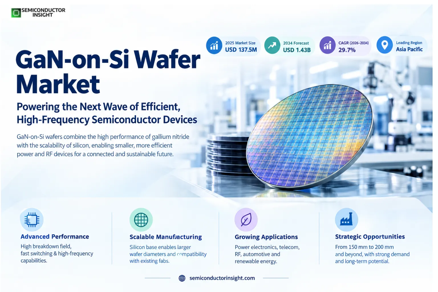
- Market trajectory: GaN-on-Si Wafer Market was valued at USD 137.5 million in 2025 and is projected to reach USD 1.43 billion by 2034, representing a 29.7% CAGR over 2026–2034.
- Largest type: 6 inch GaN-on-Si Wafer holds the strongest commercial position because established epitaxy and device flows make 150 mm production the current volume base while 200 mm scales rapidly.
- Demand center: Consumer Electronics is the principal application segment, supported by fast chargers and compact power supplies use GaN switches to improve efficiency and power density.
- Regional position: Asia Pacific leads demand as China, Taiwan, Japan and other Asian manufacturing clusters combine power-device capacity with high-volume electronics demand.
- Growth driver: Fast-charging, data-center power and RF applications are accelerating adoption of GaN devices on scalable silicon substrates.
- Primary restraint: Epitaxial stress, defect control and yield become harder as wafer diameter and voltage requirements increase.
GaN-on-Si Wafer Market Overview
GaN-on-Si wafer market was valued at USD 137.5 million in 2025 and is estimated at USD 178.4 million in 2026. It is projected to reach USD 1.43 billion by 2034, registering a CAGR of 29.7% over 2026–2034. Asia Pacific held the leading regional position in 2025.
GaN-on-Si wafers combine gallium nitride epitaxial layers with silicon substrates, enabling high-electron-mobility transistor structures for power and radio-frequency applications. The silicon base offers a path toward larger wafer diameters and compatibility with established semiconductor manufacturing infrastructure, while GaN provides high breakdown field, fast switching and strong high-frequency performance. The market therefore sits at the intersection of advanced epitaxy, compound semiconductors and silicon-scale manufacturing.
Commercial demand is strongest in power electronics, where GaN enables smaller adapters, higher switching frequencies and improved efficiency, and is expanding in telecom and RF development. The central manufacturing challenge is controlling lattice and thermal mismatch between GaN and silicon. Buffer-layer engineering, wafer bow, defect density and thermal management determine whether larger-diameter wafers can achieve the yield required for cost-effective production.
The market is moving from 150 mm toward 200 mm platforms, while 300 mm development is becoming strategically important. Larger wafers can increase die output per production run and improve compatibility with high-volume silicon tools, but the transition requires stable epitaxy and device processes. Suppliers with strong MOCVD know-how, engineered substrates and foundry partnerships are positioned to capture this scale-up.
Segment Analysis: By Type
By type, the market is segmented into 6 inch, 8 inch, 12 inch and other GaN-on-Si wafers. Six-inch wafers remain the current volume base, while eight-inch platforms are central to industrial scaling. Twelve-inch development represents the next manufacturing step as suppliers seek silicon-fab economics and higher die output.
| Type | Technical role | Market position |
|---|---|---|
| 6 inch GaN-on-Si Wafer | Mature commercial diameter for established epitaxy and device lines | Largest current segment. Broad process familiarity and installed equipment support volume manufacturing. |
| 8 inch GaN-on-Si Wafer | 200 mm platform compatible with more mainstream silicon tooling | Fast-scaling category as foundries and IDMs target higher throughput and improved cost per die. |
| 12 inch GaN-on-Si Wafer | 300 mm platform for silicon-scale manufacturing | Strategic emerging segment; requires stringent bow, stress and defect control across larger area. |
| Others | Research and specialized diameters | Used in development, niche device structures and process qualification. |
Wafer diameter changes the cost equation
Moving to larger silicon wafers increases the number of usable dies per process run and opens access to more automated wafer handling and fab infrastructure. The economic benefit is meaningful only if epitaxial uniformity and device yield remain high across the full wafer, making materials engineering a decisive part of the scaling roadmap.
Segment Analysis: By Application
By application, the market covers Consumer Electronics, Industrial, Telecom & Datacom, Automotive Electronics, Defense & Aerospace, Renewable & Energy Storage, and Others. Consumer electronics is the principal near-term demand pool, while industrial power, data centers and communications broaden the long-term opportunity.
| Application | Demand characteristics |
|---|---|
| Consumer Electronics | Fast chargers and compact adapters reward switching efficiency and high power density. |
| Industrial | Power conversion and motor-control systems value efficiency, switching speed and smaller magnetics. |
| Telecom & Datacom | Power supplies and RF research create demand for high-frequency GaN platforms. |
| Automotive Electronics | Onboard power conversion and auxiliary systems offer growth as qualification matures. |
| Defense & Aerospace | Specialized RF and power systems value performance under demanding conditions. |
| Renewable & Energy Storage | High-efficiency converters can reduce losses in distributed energy systems. |
| Others | Includes research, instrumentation and emerging power-electronics uses. |
Segment Analysis: By Device Function
Device function can be separated into Power Devices, RF Devices and Mixed/R&D Platforms. Power devices dominate commercial volume today, while RF development is expanding the addressable technology space and research platforms support new buffer, gate and integration concepts.
| Device Function | Commercial relevance |
|---|---|
| Power Devices | 650 V-class and lower-voltage switching devices for chargers, power supplies and conversion. |
| RF Devices | High-frequency HEMT platforms for future communications and related infrastructure. |
| Mixed/R&D Platforms | Pre-commercial structures used for device, materials and integration development. |
Segment Analysis: By End User
End users include IDMs, Foundries, Epitaxy/Wafer Specialists and Research Institutes. IDMs and foundries seek repeatable production economics, while specialist epitaxy suppliers compete through material quality and custom structures. Research institutes remain important in scaling new wafer diameters and RF architectures.
| End User | Commercial relevance |
|---|---|
| IDMs | Integrate epitaxy, device processing and product qualification to control performance and yield. |
| Foundries | Offer platform manufacturing to fabless GaN device designers and system innovators. |
| Epitaxy/Wafer Specialists | Supply engineered GaN-on-Si structures with controlled thickness, stress and electrical characteristics. |
| Research Institutes | Develop larger-diameter processes, RF structures and reliability knowledge before commercial transfer. |
Regional Analysis
Asia Pacific leads the GaN-on-Si Wafer Market, with regional demand shaped by different combinations of manufacturing concentration, installed-base replacement, regulatory requirements and customer qualification. The market is therefore not a uniform global pool: supplier access depends on local production ecosystems, channel depth, technical support and the purchasing model used by major customers.
How does regional demand differ across the GaN-on-Si wafer market?
Asia Pacific leads because it combines major GaN device manufacturers, compound-semiconductor expertise and the consumer-electronics supply chain that first commercialized high-volume GaN chargers. Europe has strong power-semiconductor and research capability, while North America is important in device design, data-center power and RF innovation. Regional competition is increasingly tied to 200 mm and 300 mm manufacturing readiness.
| Region | Position | Growth outlook | Demand profile | What decides supplier selection |
|---|---|---|---|---|
| Asia Pacific | Largest | High | Manufacturing and new-capacity led | Scale, qualification, local support |
| North America | Technology leader | Moderate to high | Technology and replacement led | Performance, support, compliance |
| Europe | Technology leader | Moderate | Compliance and specialty led | Compliance, sustainability, engineering |
| South America | Early-stage | Selective | Import and distributor led | Landed cost, availability, service |
| Middle East & Africa | Early-stage | Selective to high | Project and infrastructure led | Reliability, integrator support, delivery |
Key GaN-on-Si Wafer Market Manufacturers and Competitive Landscape
Competition spans epitaxy specialists, wafer suppliers, IDMs and vertically integrated GaN device manufacturers. The decisive capabilities are buffer-layer design, defect control, wafer bow management, diameter scaling and the ability to transfer epitaxy into repeatable high-yield device manufacturing.
Specialist suppliers such as IQE, Soitec-related EpiGaN assets, DOWA and other epitaxy vendors compete on material quality and customer-specific structures. Integrated device companies such as Innoscience and major semiconductor manufacturers can internalize more of the value chain, using wafer capability to support proprietary device platforms.
China has become an important manufacturing center as local firms build GaN epitaxy and device capacity for high-volume power electronics. Japan and Europe contribute deep materials and power-semiconductor expertise, while research organizations such as imec are demonstrating how GaN-on-Si can extend beyond power into RF architectures on 200 mm wafers.
Scale-up creates both opportunity and risk. A supplier that moves successfully to 200 mm or 300 mm can lower die cost and access automated silicon infrastructure, but poor uniformity or wafer bow can erase the economic benefit. Competitive advantage therefore depends on manufacturing yield as much as nominal wafer diameter.
Tier structure
| Competitive tier | Representative companies | Basis of competition |
|---|---|---|
| Integrated technology leaders | Innoscience; Sanan Optoelectronics; China Resources Microelectronics | Device-plus-epitaxy scale, high-volume power applications and manufacturing integration. |
| Epitaxy / wafer specialists | IQE; DOWA; SEDI/SCIOCS; NTT-AT; Episil-Precision | Materials quality, custom epi structures and customer qualification. |
| Emerging regional suppliers | Enkris; CorEnergy; Suzhou Nanowin; Qingdao Cohenius; Shaanxi Yuteng; IVWorks | Localized supply, process development and expanding wafer portfolios. |
Companies profiled: IQE, Soitec (EpiGaN), Transphorm, SEDI/SCIOCS, NTT-AT, DOWA, BTOZ, Episil-Precision, Epistar, Enkris, Innoscience, China Resources Microelectronics, CorEnergy, Suzhou Nanowin, Qingdao Cohenius, Shaanxi Yuteng, Sanan Optoelectronics, IVWorks.
GaN-on-Si Wafer Market Production Capacity Analysis
Production capacity depends on MOCVD epitaxy, high-quality silicon substrates and qualified semiconductor process lines. Unlike a commodity wafer market, nominal square meters of output do not fully describe usable capacity because wafer bow, epi uniformity, defect density and electrical performance determine yield at the device level.
The move to 200 mm is commercially important because it aligns GaN with a large installed base of silicon production tools. Imec has demonstrated CMOS-compatible 200 mm RF GaN-on-Si, while multiple power-device manufacturers have built 200 mm roadmaps. This broadens foundry options and can improve automation compared with smaller compound-semiconductor formats.
Three-hundred-millimeter development raises the scale further. Infineon stated in 2025 that a 300 mm wafer can yield 2.3 times more chips than a 200 mm wafer, highlighting the potential manufacturing leverage if material quality and process yield can be sustained. The transition is therefore likely to favor companies with strong materials science and capital resources.
GaN-on-Si Wafer Market Market Dynamics: Drivers, Restraints and Opportunities
The market is expanding rapidly because GaN power devices are moving into mainstream charging and power-conversion applications while larger silicon substrates offer a route to lower manufacturing cost. The counterweight is materials complexity: scaling GaN epitaxy across large silicon wafers requires careful control of thermal stress, defects and uniformity, and automotive or industrial customers add long reliability qualification cycles.
MARKET DRIVERS
Drivers Impact Analysis*
| Driver | Impact | Commercial mechanism |
|---|---|---|
| Fast charging and compact power | High | Raises demand for efficient high-frequency GaN switches. |
| 200 mm / 300 mm scaling | High | Improves potential die economics and fab compatibility. |
| Data-center and RF innovation | Medium | Expands applications beyond consumer adapters. |
Fast chargers established a high-volume entry point
GaN transistors can switch at high frequency, enabling smaller passive components and compact adapter designs while reducing power losses. Consumer charging created a practical route to scale because performance gains are visible to device makers through reduced size and improved efficiency.
Larger wafers improve manufacturing leverage
Silicon substrates offer a path toward the wafer diameters used in mainstream semiconductor fabs. Moving from 150 mm to 200 mm and later 300 mm can increase output per process run and improve automation, provided epitaxial quality and device yield remain stable.
Data-center power broadens the addressable base
AI and high-performance computing systems require efficient power conversion from grid input through rack and board-level stages. GaN can reduce switching losses in selected topologies, creating demand that is less tied to consumer charging cycles and more connected to infrastructure investment.
MARKET RESTRAINTS
Restraints Impact Analysis*
| Restraint | Impact | Commercial mechanism |
|---|---|---|
| Epitaxial stress and defects | High | Material mismatch can reduce yield and reliability. |
| Qualification requirements | Medium | Industrial and automotive adoption requires extensive reliability evidence. |
| Competing wide-bandgap platforms | Medium | GaN-on-Si competes with silicon, SiC and GaN-on-SiC depending on voltage and RF needs. |
Material mismatch complicates scaling
GaN and silicon have different lattice and thermal expansion characteristics. Buffer stacks must control stress through epitaxy and cooling, and the challenge becomes more demanding on larger wafers where bow and uniformity can affect lithography and downstream process compatibility.
Reliability qualification takes time
High-volume consumer applications can adopt quickly, but automotive and industrial customers require longer qualification, traceability and lifetime evidence. This slows the conversion of technical design wins into broad wafer demand in more conservative end markets.
Alternative technologies remain strong
Silicon MOSFETs continue improving in cost-sensitive applications, while SiC is strong at higher voltages and GaN-on-SiC remains important for demanding RF power. GaN-on-Si must therefore win where its combination of performance, wafer scale and cost is clearly superior.
MARKET OPPORTUNITIES
300 mm manufacturing
Successful 300 mm GaN-on-Si could unlock greater die output and deeper integration with high-volume silicon fabs. Early movers may secure strategic partnerships with large IDMs and foundries seeking compound-semiconductor growth on existing infrastructure.
RF GaN-on-Si for beyond-5G
Imec is developing CMOS-compatible 200 mm RF GaN-on-Si for future communications. If performance and reliability targets are met, this could extend silicon-substrate GaN into RF applications historically dominated by other substrate choices.
AI data-center power conversion
Rising rack power density makes conversion efficiency increasingly valuable. GaN suppliers can target power-supply stages where high switching frequency reduces component size and losses, linking wafer demand to rapidly expanding data-center infrastructure.
Integrated power platforms
Combining GaN power devices with drivers, protection and advanced packaging can simplify customer adoption. Wafer suppliers that coordinate epi structures with device and package requirements can become more deeply embedded in platform roadmaps.
GaN-on-Si Wafer Market Supply Chain Analysis
Silicon wafers, gallium and nitrogen precursors, MOCVD consumables.
Buffer and GaN layer growth with stress, defect and thickness control.
HEMT processing, metallization, passivation, wafer test and singulation.
Packaging, drivers, modules and final electronics integration.
Epitaxy is the critical value-creation step because material quality determines downstream device yield. MOCVD tool utilization, precursor control, wafer handling and metrology all influence the usable output from nominal wafer capacity. This makes supplier process know-how difficult to commoditize.
As wafers scale, coordination with foundry tools becomes more important. Bow limits, edge exclusion, film stress and contamination requirements must fit silicon-fab automation, so the winning supply chains are likely to connect substrate engineering, epitaxy and device process development rather than optimize each stage independently.
Recent Developments in the GaN-on-Si Wafer Market
July 2025 — Infineon advanced 300 mm GaN manufacturing
Infineon said its 300 mm GaN wafer technology can produce 2.3 times more chips per wafer than 200 mm and planned initial customer samples in the fourth quarter of 2025, signaling a major scale-up path for GaN manufacturing. Source.
2025 — imec demonstrated high-performance RF GaN-on-Si research
Imec reported progress in RF GaN-on-Si transistor performance for future 6G power amplifiers, extending the technology opportunity beyond mainstream power conversion. Source.
2025 — SEMI highlighted continued global fab construction
SEMI identified 18 new fab construction projects starting in 2025, including fifteen 300 mm facilities, supporting a broader semiconductor infrastructure base into which scalable GaN-on-Si processes can increasingly fit. Source.
REPORT SCOPE & SEGMENTATION
| Attribute | Coverage |
|---|---|
| Market | GaN-on-Si Wafer Market |
| Base Year | 2025 |
| Estimated Year | 2026 |
| Forecast Period | 2026–2034 |
| By Type | 6 inch GaN-on-Si Wafer, 8 inch GaN-on-Si Wafer, 12 inch GaN-on-Si Wafer, Others |
| By Application | Consumer Electronics, Industrial, Telecom & Datacom, Automotive Electronics, Defense & Aerospace, Renewable & Energy Storage, Others |
| By Device Function | Power Devices, RF Devices, Mixed/R&D Platforms |
| By End User | IDMs, Foundries, Epitaxy/Wafer Specialists, Research Institutes |
| Regions | North America, Europe, Asia Pacific, South America, Middle East & Africa |
| Companies Profiled | IQE, Soitec (EpiGaN), Transphorm, SEDI/SCIOCS, NTT-AT, DOWA, BTOZ, Episil-Precision, Epistar, Enkris, Innoscience, China Resources Microelectronics, CorEnergy, Suzhou Nanowin, Qingdao Cohenius, Shaanxi Yuteng, Sanan Optoelectronics, IVWorks |
Frequently Asked Questions
What is the size of the GaN-on-Si Wafer Market?
The market was valued at USD 137.5 million in 2025 and is projected to reach USD 1.43 billion by 2034, with a CAGR of 29.7% during 2026–2034.
Which region leads the market?
Asia Pacific is the largest regional market, supported by China, Taiwan, Japan and other Asian manufacturing clusters combine power-device capacity with high-volume electronics demand.
Which type leads the GaN-on-Si wafer market?
6 inch GaN-on-Si Wafer holds the leading position because established epitaxy and device flows make 150 mm production the current volume base while 200 mm scales rapidly.
Which application is the largest?
Consumer Electronics is the principal application segment, driven by fast chargers and compact power supplies use GaN switches to improve efficiency and power density.
What are the main growth drivers?
Fast charging, data-center power, larger-wafer manufacturing and emerging RF applications are the principal growth drivers.
What are the main restraints?
The main restraints are epitaxial stress and defect control, long reliability qualification and competition from silicon, SiC and GaN-on-SiC.
What additional segmentation is covered?
The analysis also covers Device Function and End User, enabling comparison beyond type and application.
How is competition structured?
Competition includes integrated GaN device makers, epitaxy specialists and wafer suppliers; yield and wafer-diameter scaling are key differentiators.
What is changing in the supply chain?
Epitaxy is the critical bottleneck, with wafer bow, film stress, uniformity and defect density determining how effectively nominal wafer capacity converts into usable device output.
Which companies are profiled?
IQE, Soitec (EpiGaN), Transphorm, SEDI/SCIOCS, NTT-AT, DOWA, BTOZ, Episil-Precision, Epistar, Enkris, Innoscience, China Resources Microelectronics, CorEnergy, Suzhou Nanowin, Qingdao Cohenius, Shaanxi Yuteng, Sanan Optoelectronics, IVWorks.
Research Sources & Evidence Base
View supporting primary and industry sources
- Infineon Technologies: 300 mm GaN manufacturing press release — 300 mm scale-up and die-output evidence.
- imec: Advanced RF technologies: RF GaN-on-Si for beyond 5G — 200 mm CMOS-compatible RF GaN-on-Si development.
- SEMI: Eighteen New Semiconductor Fabs to Start Construction in 2025 — 2025 fab-construction and capacity outlook.

Get Sample Report PDF for Exclusive Insights
Report Sample Includes
- Table of Contents
- List of Tables & Figures
- Charts, Research Methodology, and more...
 Download Sample Report PDF