Key Statistics
Key Takeaways
- Coulomb-type ESCs hold 68% of the current product mix because they provide stable, controllable wafer clamping with low leakage and are widely used across etch, deposition and wafer-handling systems.
- 300 mm wafers account for 76% of application demand, reflecting the concentration of advanced logic, DRAM, NAND and foundry production on 300 mm platforms.
- Asia Pacific is the dominant regional market through semiconductor-equipment and wafer-fab concentration in China, Taiwan, South Korea and Japan.
- SHINKO and TOTO collectively hold about 77% of the current market, demonstrating the importance of ceramic processing, electrode integration, surface engineering and long customer qualification cycles.
- AI-driven fab investment is expanding the installed base. SEMI’s Q2 2026 outlook tracks 413 300 mm fabs and lines and projects record front-end equipment spending, supporting long-term demand for wafer-handling and chamber components.
Electrostatic Chucks (ESCs) Market Overview
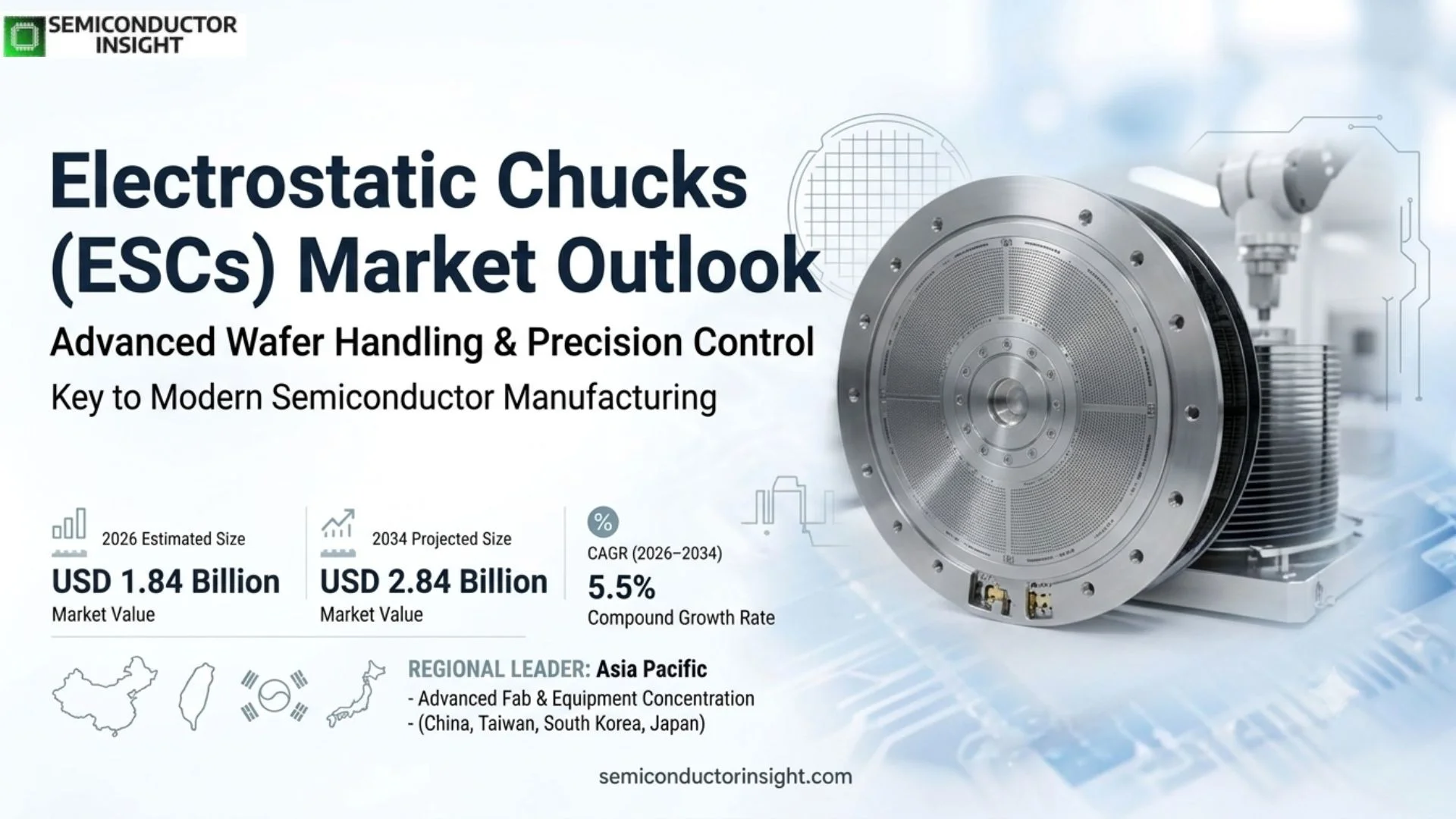
Electrostatic Chucks (ESCs) market is valued at USD 1.74 billion in 2025 and is projected to reach USD 2.84 billion by 2034, representing a 5.5% CAGR during 2026–2034. The 2026 estimated market size is USD 1.84 billion. Asia Pacific is the largest regional market because advanced semiconductor fabrication and semiconductor-equipment manufacturing are concentrated across China, Taiwan, South Korea and Japan.
An electrostatic chuck secures a semiconductor wafer using electrostatic attraction rather than mechanical clamps or vacuum contact. The chuck is typically built from high-purity ceramic with embedded electrodes and may integrate gas channels, temperature-control structures and surface textures. By maintaining flatness and controlled thermal contact during plasma processing, the ESC becomes a critical interface between the wafer and the semiconductor manufacturing tool.
Two primary clamping mechanisms are used. Coulomb-type ESCs rely on electrostatic attraction through a dielectric layer and generally provide low leakage and stable force. Johnsen-Rahbek designs use controlled electrical conduction near the wafer interface to generate stronger holding force at lower applied voltage, making them useful in selected high-force or challenging process environments. Both architectures must balance chucking force, de-chucking speed, plasma resistance and wafer damage risk.
Advanced-node manufacturing increases performance requirements. High-density plasma etch, deposition and next-generation memory processes expose ESCs to corrosive gases, large RF power and tighter wafer-temperature windows. Ceramic composition, electrode uniformity, surface roughness and backside helium-gas control influence local wafer temperature and process uniformity. These requirements make ESCs a high-value engineered component rather than a simple wafer fixture.
Segment Analysis: By Type
By type, the market is segmented into Coulomb Type and Johnsen-Rahbek (JR) Type. Coulomb-type ESCs account for 68% of the current market because they combine reliable clamping, low leakage and broad compatibility with semiconductor etch, deposition and handling systems.
| Type | Operating principle | Market position |
|---|---|---|
| Coulomb Type | An embedded electrode creates an electric field through an insulating ceramic, generating electrostatic force between the chuck and wafer. High dielectric strength helps minimize leakage current while maintaining predictable clamping behavior across repeated process cycles. | Largest type with 68% share. The architecture is widely used in advanced wafer processing where low leakage, stable temperature behavior and clean de-chucking are required. |
| Johnsen-Rahbek (JR) Type | JR ESCs use a controlled semiconductive interface that allows localized charge movement and stronger attractive force at lower applied voltage. Material resistivity and temperature must be carefully controlled to maintain consistent performance. | A strategically important segment for high holding force and selected plasma processes. Suppliers compete through ceramic resistivity control, fast release, low particle generation and process-specific surface engineering. |
Material and operating-function segmentation
The market can also be segmented by ceramic material and ESC functionality. Alumina offers strong insulation, plasma resistance and cost effectiveness, while aluminum nitride is selected where higher thermal conductivity and tighter wafer-temperature uniformity are required. Advanced ESCs may integrate heating, backside gas distribution, embedded sensors or multi-zone temperature control.
| Axis | Segments | Commercial implication |
|---|---|---|
| By Ceramic Material | Alumina · Aluminum Nitride · Other Engineered Ceramics | Alumina supports broad Coulomb and JR designs; aluminum nitride is favored where thermal conductivity and temperature uniformity are especially important; specialty ceramics target extreme plasma or electrical requirements. |
| By Functional Integration | Clamping-Only ESC · Temperature-Control ESC · Heater-Integrated ESC · Sensor-Enabled ESC | More process functions are moving into the chuck, increasing value per unit while raising manufacturing complexity, reliability requirements and customer qualification time. |
Segment Analysis: By Application
By application, 300 mm wafers account for 76% of the current market, followed by 200 mm and other wafer sizes. The dominance of 300 mm reflects its use in leading-edge foundry, memory and high-volume semiconductor production, where equipment utilization and process uniformity justify higher-value ESC systems.
| Application | Key market insight |
|---|---|
| 300 mm Wafer | The largest application with 76% share. Advanced logic, DRAM, HBM-related front-end processes and 3D NAND use 300 mm platforms and require highly uniform wafer clamping and temperature control. SEMI tracks more than 400 300 mm fabs and lines globally, reinforcing the size of the installed equipment base. |
| 200 mm Wafer | Power semiconductors, analog, MEMS, sensors and mature-node products maintain significant 200 mm production. ESC replacement and retrofit demand remains durable because many fabs operate mature tool sets for long periods. |
| Other Wafer Sizes | Compound-semiconductor, research and specialty processes can use smaller or non-standard wafers. These applications create lower volume but may require highly customized ESC geometry, materials or temperature capability. |
| Etch Equipment | Etch is a core ESC application because plasma exposure and wafer-temperature control directly affect critical dimensions and profile. Advanced memory and logic processes place especially high demands on plasma-resistant ceramics and uniform clamping. |
| Deposition Equipment | CVD, PVD and ALD tools use ESCs or related ceramic susceptors to stabilize wafers during thin-film growth. Temperature uniformity and chemical resistance are essential for film thickness and material consistency. |
Regional Analysis
Asia Pacific dominates the Electrostatic Chucks market through the concentration of semiconductor fabs and semiconductor-equipment supply chains in China, Taiwan, South Korea and Japan. North America is expanding rapidly through U.S. fab investment, while Europe remains important in power, analog and semiconductor-equipment technologies.
How do regional ESC demand patterns differ?
ESC demand follows installed wafer-fabrication equipment and new fab investment. Asia Pacific has the largest installed base and the deepest ceramics and equipment supply network. North America is adding new advanced-node and memory capacity, Europe is expanding automotive and power semiconductor production, and emerging regions create selective demand only when front-end wafer manufacturing reaches meaningful scale.
| Region | Market position | Growth outlook | Core demand | Commercial priority |
|---|---|---|---|---|
| Asia Pacific | Largest | High | Foundry, memory & equipment | Advanced-node reliability and production scale |
| North America | Fast-expanding | High | Logic, memory & domestic fabs | Local support and high-performance ESCs |
| Europe | Specialty growth | Moderate to high | Power, analog & automotive | Lifecycle, plasma durability and precision |
| South America | Small | Selective | Research & specialty | Availability and equipment installed base |
| Middle East & Africa | Emerging | Selective | Existing / future fabs | Local ecosystem and service |
Competitive Landscape
Key participants include Applied Materials, Lam Research, SHINKO, TOTO, Sumitomo Osaka Cement, Creative Technology Corporation, Kyocera, Entegris, NTK CERATEC, NGK Insulators, II-VI M Cubed, Tsukuba Seiko, Calitech, Beijing U-PRECISION TECH and Hebei Sinopack Electronic Technology. SHINKO and TOTO collectively hold about 77% of the current market, creating a highly concentrated competitive structure.
SHINKO is a leading specialist in ceramic ESCs and integrates ceramic firing, precision machining, assembly and inspection. Its current products support Coulomb and Johnsen-Rahbek architectures, 300 mm wafers and a wide operating-temperature range. This vertically controlled ceramic process capability is a major barrier to entry.
Kyocera supplies ESCs using alumina and aluminum nitride for 200 mm and 300 mm semiconductor equipment. Its broader fine-ceramics portfolio includes chambers, heaters, vacuum chucks and handling arms, enabling material and manufacturing knowledge to be shared across multiple wafer-processing components.
NGK is increasing U.S. semiconductor-component investment and highlights ESC performance in high-power plasma environments. Applied Materials and Lam Research integrate wafer-handling technology into equipment platforms, while regional Chinese suppliers seek qualification as semiconductor equipment localization expands.
Competitive tier structure
| Competitive tier | Representative companies | Competitive strengths |
|---|---|---|
| Global ESC leaders | SHINKO; TOTO | High market share, advanced ceramic processing, long fab qualifications and 300 mm capability |
| Advanced ceramic specialists | Kyocera; NGK Insulators; NTK CERATEC; Sumitomo Osaka Cement; II-VI M Cubed | Plasma-resistant ceramics, thermal control, integrated heaters and precision material engineering |
| Equipment / regional participants | Applied Materials; Lam Research; Entegris; Tsukuba Seiko; Calitech; U-PRECISION; Sinopack | Tool integration, replacement components, regional customer proximity and semiconductor localization |
Key companies profiled
ESC Manufacturing Capacity & Qualification Analysis
ESC production capacity depends on ceramic powder preparation, forming, electrode integration, high-temperature firing, precision machining, surface treatment, bonding, electrical inspection and thermal characterization. The process is capital intensive and yield sensitive because a defect discovered after firing or final machining can scrap a high-value component.
300 mm ESCs are especially demanding because wafer-scale flatness and temperature uniformity must be maintained across a large diameter. Multi-zone electrodes, gas grooves and embedded thermal functions increase the number of precision operations. Capacity growth therefore requires skilled ceramic engineering and metrology as well as additional furnaces or machining equipment.
Customer qualification creates an effective capacity barrier. A semiconductor-equipment OEM validates chucking force, particle behavior, plasma durability, RF performance and temperature uniformity before production use. A newly built factory cannot immediately substitute for an approved line without process-equivalence and reliability testing.
Market Dynamics
Growth is driven by global fab expansion, advanced-node etch and deposition, 300 mm wafer adoption, HBM/memory investment and equipment automation. Restraints include manufacturing complexity, high qualification barriers, ceramic-material cost and market concentration. Opportunities center on advanced plasma-resistant ceramics, integrated thermal control, local production and ESCs for next-generation wafer processes.
MARKET DRIVERS
Fab expansion increases installed tool count
Every new etch, deposition and selected handling tool creates initial and replacement ESC demand. SEMI’s 2026 outlook shows sustained record investment in 300 mm manufacturing, directly expanding the installed base.
Advanced nodes require tighter wafer control
Smaller features and deeper 3D structures make process uniformity more sensitive to wafer temperature and position. ESC flatness, backside gas distribution and thermal control therefore become more valuable.
Memory processes increase plasma intensity
3D NAND, DRAM and HBM-related production use repeated etch and deposition steps. More chamber cycles increase wear on plasma-facing components and support higher replacement demand.
Automation rewards fast, repeatable clamping
High-volume fabs need consistent chuck and de-chuck behavior with minimal wafer damage. Reliable ESC performance helps protect tool throughput and reduces handling interruptions.
Drivers Impact Analysis
| Driver | Impact | Primary markets | Time horizon |
|---|---|---|---|
| 300 mm fab investment | High | Asia Pacific, U.S., Europe | Medium to long term |
| Advanced-node plasma etch | High | Leading-edge logic & memory | Persistent |
| HBM / memory capacity | High | Korea, Taiwan, U.S. | Medium term |
| Tool automation and uptime | Medium to high | Global fabs | Persistent |
MARKET RESTRAINTS
Ceramic ESC manufacturing is difficult to scale
Embedded electrodes, dense ceramics and tight machining tolerances must survive harsh plasma and thermal cycling. Yield loss at late stages makes new capacity expensive.
Qualification limits rapid supplier switching
A new ESC can affect particles, wafer temperature and process results. Semiconductor equipment suppliers therefore require extensive validation before changing a qualified component.
Energy-intensive firing affects cost
High-purity ceramic processing uses high-temperature furnaces and specialized raw materials. Energy and material cost can pressure margins, especially in lower-volume customized designs.
Market concentration raises entry barriers
Leading suppliers have decades of field data and customer process knowledge. New entrants must match both technical performance and long-term reliability before winning production programs.
Restraints Impact Analysis
| Restraint | Impact | Exposure | Time horizon |
|---|---|---|---|
| Complex ceramic manufacturing | High | Global suppliers | Persistent |
| Long qualification cycles | High | Equipment OEMs / fabs | Persistent |
| Raw-material and energy cost | Medium | Ceramic production | Short to medium term |
| High market concentration | Medium to high | Global | Persistent |
MARKET OPPORTUNITIES
Develop next-generation plasma-resistant surfaces
Higher RF power and aggressive etch chemistry create demand for ceramics and coatings that reduce erosion, particles and metal contamination.
Integrate more thermal-control functions
Heater zones, sensors and optimized backside gas channels can improve wafer-temperature uniformity and raise value per ESC.
Localize near new semiconductor regions
U.S. and European fab expansion creates opportunities for local production, refurbishment and rapid field support.
Support compound-semiconductor and specialty wafers
SiC, GaN and other specialty processes can require customized chuck materials, surface designs and temperature ranges beyond mainstream silicon wafers.
Electrostatic Chuck Value Chain Analysis
High-purity ceramic materials
Electrode integration & firing
Precision machining & surface engineering
Tool qualification & fab use
Material purity determines contamination performance
Plasma can expose or erode ceramic surfaces, making trace metals and particle generation critical. High-purity starting powders and controlled sintering protect wafer quality.
Electrode uniformity controls chucking force
Embedded electrode geometry must create even electrostatic attraction across the wafer. Local variation can cause wafer bow or unstable thermal contact.
Surface engineering affects thermal and mechanical behavior
Groove patterns distribute backside helium gas, while roughness and embossing influence contact area and de-chucking. Small design changes can materially alter process performance.
Qualification embeds the supplier in the tool platform
Once an ESC is approved, equipment recipes and maintenance practices are built around its behavior. This creates long design cycles and strong customer retention for reliable suppliers.
Recent Developments in the Electrostatic Chucks (ESCs) Market
SEMI raises 300 mm memory equipment outlook
SEMI projected memory-sector 300 mm equipment spending above USD 50 billion in 2026, supported by HBM, DDR5 and AI infrastructure. More advanced memory equipment expands the installed base for high-performance ESCs.
SEMI tracks 413 global 300 mm fabs and lines
The latest 300 mm Fab Outlook projects record front-end equipment investment and continuing capacity expansion through the decade, reinforcing long-term wafer-handling component demand.
NGK expands semiconductor-component capability in Arizona
NGK outlined a USD 64 million Arizona investment and highlighted ESCs that maintain stable holding force in high-power plasma for advanced semiconductor etching.
Kyocera supplies plasma-resistant ESCs for 200 mm and 300 mm equipment
Kyocera’s current ESC portfolio uses alumina and aluminum nitride and supports wafer holding, flatness correction and cooling.
SHINKO supports Coulomb and JR ESC designs to 300 mm
SHINKO’s current ceramic ESC platform covers etch, ashing, CVD and PVD applications and supports operation from -20°C to +200°C.
REPORT SCOPE & SEGMENTATION
| Attribute | Details |
|---|---|
| Study Period | 2020–2034 |
| Base Year | 2025 |
| Estimated Year | 2026 |
| Forecast Period | 2026–2034 |
| Historical Period | 2020–2025 |
| Market Size 2025 | USD 1.74 billion |
| Market Size 2034 | USD 2.84 billion |
| Growth Rate | 5.5% during 2026–2034 |
| Unit | Value (USD Million/Billion) and ESC unit shipments |
| By Type | Coulomb Type · Johnsen-Rahbek (JR) Type |
| By Application | 300 mm Wafer · 200 mm Wafer · Others |
| By Ceramic Material | Alumina · Aluminum Nitride · Other Engineered Ceramics |
| By Functional Integration | Clamping-Only ESC · Temperature-Control ESC · Heater-Integrated ESC · Sensor-Enabled ESC |
| By Region | Each region analysed by ESC type, wafer size, ceramic material, functional integration and country manufacturing ecosystem North AmericaUnited States, Canada, Mexico EuropeGermany, France, Italy, United Kingdom and other European markets Asia PacificChina, Taiwan, South Korea, Japan, Singapore and other Asian markets South AmericaBrazil, Argentina and other South American markets Middle East & AfricaIsrael, Saudi Arabia, UAE, South Africa and other MEA markets |
| Key Companies Profiled | Applied Materials · Lam Research · SHINKO · TOTO · Sumitomo Osaka Cement · Creative Technology Corporation · Kyocera · Entegris · NTK CERATEC · NGK Insulators · II-VI M Cubed · Tsukuba Seiko · Calitech · Beijing U-PRECISION TECH · Hebei Sinopack Electronic Technology |
| Customization Scope | Free report customization equivalent to up to four analyst working days with purchase. Addition or alteration to country, regional and segment scope. |
Frequently Asked Questions
What is the 2025 size of the Electrostatic Chucks market?
The market is valued at USD 1.74 billion in 2025 and is projected to reach USD 2.84 billion by 2034. The 2026 estimate is USD 1.84 billion and the 2026–2034 CAGR is 5.5%, reflecting continued semiconductor-fab and equipment expansion.
Which ESC type leads the market?
Coulomb-type ESCs lead with 68% share. Their stable clamping, low leakage and broad process compatibility make them suitable for etch, deposition and wafer-handling applications across advanced and mature semiconductor manufacturing.
Which wafer size is the largest application?
300 mm wafers account for 76% of current demand. Advanced logic, DRAM, NAND and leading foundry production are concentrated on 300 mm platforms, increasing the installed base of equipment that requires high-performance electrostatic chucks.
Which region leads the market?
Asia Pacific is the largest regional market because China, Taiwan, South Korea and Japan have the greatest concentration of semiconductor fabs, memory manufacturing and semiconductor-equipment supply chains.
What is the estimated market size in 2026?
The 2026 estimated market size is USD 1.84 billion. Growth is supported by record 300 mm equipment investment, advanced-node process requirements and high-intensity memory manufacturing.
What is the difference between Coulomb and Johnsen-Rahbek ESCs?
Coulomb designs use electrostatic attraction across a dielectric ceramic, while Johnsen-Rahbek designs use controlled semiconductive behavior near the interface to generate stronger holding force at lower voltage. Each architecture is optimized for different process conditions.
Why are ceramics used in ESCs?
High-purity alumina and aluminum nitride provide electrical insulation, plasma resistance and dimensional stability. Aluminum nitride also offers high thermal conductivity, which is useful where wafer-temperature uniformity is especially demanding.
What are the main market restraints?
The main restraints are complex ceramic manufacturing, long semiconductor qualification cycles, high energy and material cost, and strong concentration among established suppliers with deep process knowledge.
How does AI affect ESC demand?
AI accelerates investment in advanced logic, HBM and memory fabs. More etch and deposition equipment increases initial and replacement demand for ESCs, while advanced processes require tighter wafer-temperature and plasma-performance specifications.
What does the report cover?
The report covers Coulomb and Johnsen-Rahbek ESCs; 300 mm, 200 mm and other wafer applications; ceramic materials and integrated functions; five global regions; manufacturing analysis; market dynamics; recent developments; and the major companies active in the market.
Research Sources & Evidence Base
View primary and authoritative evidence used in this overview
- SHINKO Electric Industries. Ceramic Electrostatic Chuck – Official specifications covering Coulomb and JR types, 300 mm size capability, temperature range and semiconductor-tool applications.
- Kyocera. Electrostatic Chucks – Official product information on alumina and aluminum-nitride ESCs for 200 mm and 300 mm equipment.
- NGK Insulators. FY2025 First-Half Results – Primary company evidence on ESC performance in high-power plasma and Arizona semiconductor-component capacity investment.
- SEMI. 300mm Fab Outlook – Q2 2026 – Industry evidence on global 300 mm fab count, equipment investment and capacity expansion.
- Kyocera. Ceramic Components for Semiconductor Processing – Official overview of ESCs, heaters, vacuum chucks, chambers and related ceramic technologies for semiconductor tools.
Get Sample Report PDF for Exclusive Insights
Report Sample Includes
- Table of Contents
- List of Tables & Figures
- Charts, Research Methodology, and more...
 Download Sample Report PDF