
Semiconductor Equipment for Advanced Packaging Market Insights
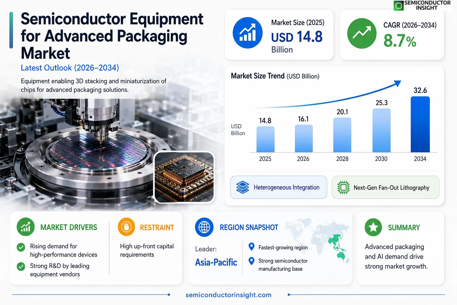
Global semiconductor equipment for advanced packaging market size was valued at USD 14.8 billion in 2026. The market is projected to grow from USD 14.8 billion in 2026 to USD 32.6 billion by 2034, exhibiting a CAGR of 8.7% during the forecast period.
Semiconductor equipment for advanced packaging comprises wafer‑level fan‑out (FOWLP), chip‑on‑wafer (CoW), heterogeneous integration tools, die‑attach systems, and high‑precision inspection and metrology solutions that enable three‑dimensional stacking and miniaturization of chips.The market is experiencing rapid growth because demand for high‑performance computing, AI accelerators, and mobile devices drives adoption of multi‑chip modules and system‑in‑package solutions. However, supply chain constraints on critical materials pose challenges, while continued investment in R&D by leading vendors such as Applied Materials, ASML, Lam Research, Tokyo Electron and KLA Corp fuels expansion. Furthermore, recent announcementslike Applied Materials’ March 2024 launch of a next‑generation fan‑out lithography platformillustrate how innovation is accelerating deployment of advanced packaging technologies worldwide.
MARKET DRIVERS
Rising Demand for High‑Performance Miniaturized Devices
Semiconductor Equipment for Advanced Packaging Market is being propelled by the surge in consumer electronics that require higher performance in smaller form factors. 3D‑IC and fan‑out wafer‑level packaging (FOWLP) technologies enable chip‑on‑chip interconnects, delivering up to 30% improvement in signal speed and 15% reduction in power consumption.
Investment in R&D by Leading Equipment Vendors
Major OEMs are allocating over $2 billion annually to develop next‑generation lithography and deposition tools tailored for advanced packaging. This capital infusion shortens time‑to‑market for new package architectures, fostering a competitive ecosystem.
➤ Strategic partnerships between equipment manufacturers and foundries accelerate technology transfer, driving a compound annual growth rate (CAGR) of roughly 12% through 2028.
Regulatory incentives in key regions, such as tax credits for domestic chip production, further bolster the market by lowering total cost of ownership for end users.
MARKET CHALLENGES
Complexity of Integration Across Heterogeneous Materials
Integrating diverse material stacks (silicon, glass, organic substrates) within a single package increases process variability, leading to lower yields. Operators often experience 5‑7% yield loss during the pilot phase, which inflates capital expenditures.
Other Challenges
Talent Shortage
The specialized skill set required for advanced packaging equipment maintenance is scarce, with an estimated shortfall of 1,200 engineers globally, driving up labor costs and extending equipment downtime.
MARKET RESTRAINTS
High Up‑Front Capital Requirements
Acquiring a single advanced deposition line can exceed $150 million, creating a financial barrier for mid‑size foundries. This capital intensity limits market participation and slows adoption of cutting‑edge packaging solutions.Additionally, the long payback periodoften beyond five yearsdiscourages investment in regions with volatile demand cycles.Supply chain disruptions for critical components such as high‑purity gases further constrain production capacity, reinforcing the restraint.
MARKET OPPORTUNITIES
Emergence of Chiplet‑Based Architectures
Chiplet designs require sophisticated interposer and redistribution layer (RDL) equipment, opening a sizeable niche for vendors that can deliver high‑throughput, sub‑micron alignment tools. Forecasts suggest this segment could capture $4 billion of revenue by 2027.The acceleration of automotive electrification creates demand for robust power‑module packaging, presenting an opportunity for equipment providers to tailor solutions for high‑temperature, high‑reliability applications.Finally, the rollout of 5G and early 6G trials amplifies the need for millimeter‑wave antennas integrated within advanced packages, driving a new wave of equipment sales focused on low‑loss material processing.
Semiconductor Equipment for Advanced Packaging Market Trends
Rapid Adoption of Fan‑Out Wafer‑Level Packaging (FOWLP)
Semiconductor Equipment for Advanced Packaging Market is witnessing a pronounced shift toward fan‑out wafer‑level packaging (FOWLP) as manufacturers target higher I/O density and thinner form factors for AI accelerators and high‑performance computing modules. Recent platform launches from leading vendors have streamlined lithography steps, reducing cycle time and enabling finer line widths that support the next generation of multi‑chip modules. This technology advantage is driving broader implementation across mobile, data‑center, and automotive segments, where performance per watt and form‑factor efficiency are critical differentiators.
Other Trends
Supply Chain Constraints on Critical Materials
Despite strong demand, Semiconductor Equipment for Advanced Packaging Market faces material bottlenecks, particularly for high‑purity photoresists and advanced carrier tapes used in fan‑out processes. Manufacturers are responding by diversifying supplier bases and increasing on‑site inventory buffers, yet short‑term lead‑time volatility remains a risk factor that can affect production scheduling and cost structures across the ecosystem.
Increased Investment in Heterogeneous Integration Tools
Another salient trend is the accelerating investment in heterogeneous integration equipment, which enables the stacking of logic, memory, and specialty dies within a single package. Companies such as Applied Materials, ASML, and Lam Research have reported expanded R&D roadmaps that focus on precision die‑attach, high‑resolution metrology, and automated inspection solutions. These capabilities are essential for realizing dense three‑dimensional architectures that meet the performance demands of next‑generation AI workloads.
COMPETITIVE LANDSCAPEKey Industry Players
Semiconductor Equipment for Advanced Packaging – Competitive Landscape Overview
The advanced packaging segment of the semiconductor equipment market is dominated by a handful of global innovators that together account for more than half of the 2026 market value of USD 14.8 billion. Applied Materials leads with its next‑generation fan‑out lithography platform, leveraging deep R&D investment to capture high‑growth AI and HPC demand. ASML supplies extreme‑ultraviolet (EUV) and next‑generation lithography tools essential for wafer‑level fan‑out (FOWLP) processes, while Lam Research and Tokyo Electron provide critical deposition, etch, and cleaning equipment that underpin heterogeneous integration. KLA Corporation complements the ecosystem with high‑precision inspection and metrology solutions that ensure yield in three‑dimensional stacking. The collective emphasis on scalability, throughput, and cost‑of‑ownership shapes a market structure where tier‑one vendors drive technology roadmaps and secure long‑term supply contracts with major foundries.Beyond the tier‑one cohort, a diverse set of niche specialists expands the functional breadth of the advanced packaging supply chain. SCREEN Holdings offers wafer‑level bonding and polymer deposition systems that are particularly valuable for fan‑out wafer‑level packaging. Canon Tokki remains a leader in organic light‑emitting diode (OLED) and die‑attach equipment, supporting emerging chip‑on‑wafer (CoW) applications. Advantest and Teradyne provide test and measurement platforms that validate multi‑chip modules, while Hitachi High‑Technologies and Nordson supply precision die‑attach and dispensing tools for heterogeneous integration. Regional players such as SUSS MicroTec contribute advanced lithography and wafer‑handling technologies, reinforcing a competitive landscape that blends large‑scale innovation with highly specialized capabilities.
List of Key Semiconductor Equipment for Advanced Packaging Companies Profiled
- Applied Materials
- ASML Holding
- Lam Research
- Tokyo Electron
- KLA Corporation
- SCREEN Holdings
- Canon Tokki
- Advantest
- Teradyne
- Hitachi High‑Technologies
- Nordson
- SUSS MicroTec
Segment Analysis:
| Segment Category | Sub-Segments | Key Insights |
| By Type |
|
Advanced Fan‑Out Solutions are emerging as the leading type because they enable fine‑pitch interconnects and high density routing without increasing form factor.
|
| By Application |
|
AI Accelerator Packages dominate this dimension as designers increasingly rely on multi‑chip stacking to meet AI model complexity.
|
| By End User |
|
Leading Foundries are the primary end‑users because they drive volume production and standardize advanced packaging processes.
|
| By Technology |
|
Next‑Generation Lithography is perceived as the most transformative technology, enabling finer line widths and tighter pitch.
|
| By Process Stage |
|
Bonding & Interconnect Formation commands attention because it directly influences electrical performance and mechanical reliability.
|
Regional Analysis: North America
United States
The semiconductor equipment manufacturing landscape in the US is characterized by a mix of established giants and innovative startups. Key players are investing heavily in R&D to develop next-generation packaging solutions. Competition is intense, with companies focusing on differentiated technologies and strong customer relationships.
The adoption of advanced packaging technologies such as 2.5D and 3D integration is a major trend driving the semiconductor equipment market. Chiplet architectures are gaining traction, requiring specialized equipment for interconnect and testing. Focus on enhancing performance, power efficiency, and miniaturization in advanced packaging is paramount.
Significant investments are being directed towards semiconductor equipment R&D and manufacturing facilities within the US. Government funding and private equity are fueling innovation and expansion in the sector. This influx of capital is fostering the development of new technologies and enhancing the competitiveness of the US semiconductor equipment industry.
The US is actively working to strengthen its semiconductor equipment supply chain, reducing reliance on foreign sources. Onshoring and nearshoring initiatives are gaining momentum to ensure a secure and resilient supply of critical components and equipment.
Europe
Europe represents a significant market for semiconductor equipment, driven by a strong presence of leading semiconductor manufacturers and a growing focus on advanced packaging. The region is witnessing increased investment in R&D and manufacturing capabilities to maintain its competitiveness. Key trends include the development of innovative packaging solutions for automotive and industrial applications, alongside continued advancements in consumer electronics. Government initiatives across Europe are supporting the growth of the semiconductor equipment sector through funding programs and strategic partnerships. The emphasis is on sustainable manufacturing practices and reducing the environmental impact of semiconductor equipment production. Business strategies involve fostering collaborations between equipment suppliers and semiconductor companies to address the evolving needs of the market.
Asia-Pacific
Asia-Pacific, particularly China, presents the largest and fastest-growing market for semiconductor equipment. The region’s burgeoning semiconductor industry, driven by increasing demand for consumer electronics, automotive, and industrial applications, is fueling significant growth in the semiconductor equipment sector. China is investing heavily in domestic semiconductor equipment manufacturing capabilities, aiming to reduce its reliance on imports. Key trends include the adoption of advanced packaging technologies for mobile devices, AI, and data centers. While competitive pressures are intense, the Asia-Pacific market offers substantial opportunities for semiconductor equipment suppliers with innovative technologies and strong local partnerships.
South America
South America represents a smaller but growing market for semiconductor equipment. The increasing adoption of electronics in various industries, including telecommunications, automotive, and healthcare, is driving demand for advanced packaging solutions. The region’s focus on developing its own semiconductor capabilities presents opportunities for semiconductor equipment suppliers to establish a foothold in the market. Key trends involve the adoption of cost-effective packaging solutions for emerging applications. Business strategies often involve partnerships with local distributors and system integrators to serve the specific needs of the South American market.
Middle East & Africa
The Middle East & Africa region presents a nascent but promising market for semiconductor equipment. The increasing investment in infrastructure development, telecommunications, and industrialization is driving demand for electronics and associated packaging solutions. The region’s focus on diversifying its economy and fostering technological advancement is creating opportunities for semiconductor equipment suppliers. Key trends include the adoption of robust and reliable packaging solutions for harsh operating environments. Business strategies involve adapting to the specific requirements of the region’s growing industries and establishing long-term partnerships with local players.
Report Scope
This market research report provides a comprehensive analysis of the Semiconductor Equipment for Advanced Packaging Market , covering the forecast period 2026–2034. It offers detailed insights into market dynamics, technological advancements, competitive landscape, and key trends shaping the industry.
Key focus areas of the report include:
- Market Overview: The report begins with an overview outlining its current market scenario, key growth indicators, and industry transformation drivers. It discusses macroeconomic factors, demand–supply balance, regulatory landscape, and the strategic role of semiconductors in powering advancements across industries such as automotive, telecommunications, consumer electronics, and industrial automation.
- Market Size & Forecast: Historical data and future projections for revenue, unit shipments, and market value across major regions and segments.
- Segmentation Analysis: Detailed breakdown by product type, technology, application, and end-user industry to identify high-growth segments and investment opportunities.
- Regional Insights: Insights into market performance across North America, Europe, Asia-Pacific, Latin America, and the Middle East & Africa, including country-level analysis where relevant.
- Competitive Landscape: Profiles of leading market participants, including their product offerings, R&D focus, manufacturing capacity, pricing strategies, and recent developments such as mergers, acquisitions, and partnerships.
- Technology Trends & Innovation: Assessment of emerging technologies, integration of AI/IoT, semiconductor design trends, fabrication techniques, and evolving industry standards.
- Market Drivers & Restraints: Evaluation of factors driving market growth along with challenges, supply chain constraints, regulatory issues, and market-entry barriers.
- Stakeholder Insights: Insights for component suppliers, OEMs, system integrators, investors, and policymakers regarding the evolving ecosystem and strategic opportunities.
Primary and secondary research methods are employed, including interviews with industry experts, data from verified sources, and real-time market intelligence to ensure the accuracy and reliability of the insights presented.
FREQUENTLY ASKED QUESTIONS:
What is the current market size of Semiconductor Equipment for Advanced Packaging Market?
-> Semiconductor Equipment for Advanced Packaging Market was valued at USD 14.8 billion in 2026 and is expected to reach USD 32.6 billion by 2034, exhibiting a CAGR of 8.7% during the forecast period.
Which key companies operate in Semiconductor Equipment for Advanced Packaging Market?
-> Key players include Applied Materials, ASML, Lam Research, Tokyo Electron, and KLA Corp, among others.
What are the key growth drivers?
-> Key growth drivers include high‑performance computing, AI accelerators, mobile device demand, and the increasing adoption of multi‑chip modules and system‑in‑package solutions.
Which region dominates the market?
-> Asia‑Pacific is the fastest‑growing and dominant region, supported by strong semiconductor manufacturing ecosystems.
What are the emerging trends?
-> Emerging trends include heterogeneous integration, next‑generation fan‑out lithography, AI‑driven design automation, and advanced inspection and metrology solutions.

Get Sample Report PDF for Exclusive Insights
Report Sample Includes
- Table of Contents
- List of Tables & Figures
- Charts, Research Methodology, and more...
 Download Sample Report PDF


