
Copper Pillar Bump (Cu Bump) Market Insights
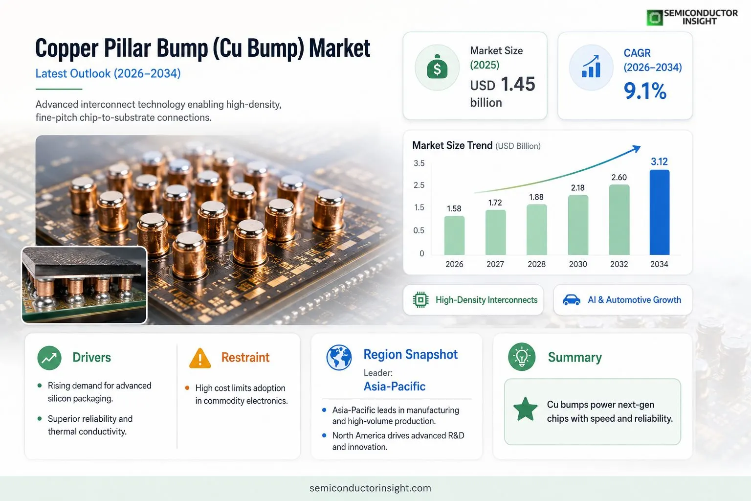
Global Copper Pillar Bump (Cu Bump) market size was valued at USD 1.45 billion in 2025. The market is projected to grow from USD 1.58 billion in 2026 to USD 3.12 billion by 2034, exhibiting a CAGR of 9.1% during the forecast period.
The Copper Pillar Bump (Cu Bump) is an advanced interconnect technology used primarily in semiconductor packaging, enabling high-density and fine-pitch connections between chips and substrates. Unlike traditional solder bumps, Cu bumps offer superior electrical performance, thermal conductivity, and mechanical reliability, making them essential for applications in high-performance computing, mobile devices, automotive electronics, and AI-driven hardware. These bumps consist of a copper pillar capped with a solder layer, facilitating precise alignment and robust bonding during flip-chip assembly processes.
While the demand for miniaturized and power-efficient electronic components continues to rise, Copper Pillar Bump (Cu Bump) Market is witnessing accelerated adoption due to its ability to support finer pitch requirements,often below 50 micrometers,and higher input/output (I/O) densities. Furthermore, advancements in heterogeneous integration and system-in-package (SiP) solutions are reinforcing the need for reliable Cu bump technologies. Industry leaders such as Taiwan Semiconductor Manufacturing Company (TSMC), Intel Corporation, Amkor Technology, and Advanced Semiconductor Engineering (ASE) are actively investing in R&D to enhance Cu bump scalability and performance.
MARKET DRIVERS
Rising Demand for Advanced Silicon Packaging
Copper Pillar Bump (Cu Bump) Market is experiencing robust growth driven by the increasing complexity of semiconductor devices and the need for miniaturization. As mobile electronics and consumer gadgets demand finer line widths and spaces, the robust mechanical properties of Cu Bumps have made them the preferred alternative to traditional solder bumps for applications below 20 nanometers.
Enhanced Reliability and Thermal Conductivity
One of the primary catalysts for Copper Pillar Bump (Cu Bump) Market expansion is the superior performance of copper in thermal management and stress mitigation. The copper pillars offer a stable alloy interface that withstands thermal cycling better than lead-based alternatives, ensuring long-term reliability for critical electronic systems.
➤ Market analysts predict that the shift towards fine-pitch interconnects will sustain the growth trajectory for Copper Pillar Bumps in high-end computing.
Furthermore, the increasing adoption of System-in-Package (SiP) technologies fuels the demand for these high-density interconnects across the 5G ecosystem.
MARKET CHALLENGES
High Capital Expenditure Requirements
Copper Pillar Bump (Cu Bump) Market faces significant operational hurdles due to the substantial capital expenditure associated with advanced packaging fabs. Establishing the infrastructure required for precise electroplating and photoresist patterning presents a barrier to entry for smaller manufacturers.
Other Challenges
Process Complexity and Yield Issues
Maintaining high production yields during the fabrication of microscopic interconnects remains a persistent challenge for leading foundries, complicating supply chain stability.
MARKET RESTRAINTS
Saturation in Commodity Electronics
Copper Pillar Bump (Cu Bump) Market is currently restrained by the cost sensitivity of the commodity electronics sector, where traditional solder bumps remain the viable standard. Manufacturers in lower-end applications often find the premium cost of Cu Bump technology prohibitive, slowing down widespread adoption in those segments.
MARKET OPPORTUNITIES
Exponential Growth in AI and Automotive Applications
Copper Pillar Bump (Cu Bump) Market holds immense potential for growth through the electrification of the automotive industry and the exponential development of artificial intelligence. Vehicles and data centers require high-bandwidth interconnects that can withstand vibration and thermal stress, making Cu Bumps essential for advanced driver-assistance systems (ADAS) and high-performance computing accelerators.
Copper Pillar Bump (Cu Bump) Market Trends
Innovations in High-Density Interconnect Technology
Technological evolution in electronic hardware is reshaping market dynamics, with interconnect solutions playing a pivotal role. The copper pillar bump technology is emerging as an advanced interconnect solution used primarily in semiconductor packaging. It enables high-density and fine-pitch connections between chips and substrates. By offering superior electrical performance, thermal conductivity, and mechanical reliability, this methodology distinguishes itself from traditional solder bumps. As Global landscape shifts toward energy efficiency, the demand for these robust connections is accelerating across high-performance computing, mobile devices, and automotive electronics sectors.
Other Trends
Facilitating Heterogeneous Integration Processes
The modern electronic ecosystem requires complex integration strategies. The market observes a significant trend where copper pillars, often capped with a solder layer, facilitate precise alignment and robust bonding during flip-chip assembly. This physical structure supports finer pitch requirements, frequently pushing below 50 micrometers, and allows for higher input/output (I/O) densities. As companies pursue smaller, more powerful components, the need for these fine-pitch structures remains a critical driver for industry growth and product longevity.
Strategic Investment by Semiconductor Leaders
Advancements in technology are largely driven by investments from key manufacturers. Major entities are focusing on enhancing scalability and performance to meet complex market demands. Industry leaders are actively increasing R&D efforts to support the broader ecosystem of AI-driven hardware and advanced packaging. This collaborative approach between technology providers ensures that the capabilities of the Copper Pillar Bump market continue to match the rigorous requirements of modern application development.
COMPETITIVE LANDSCAPE
Key Industry Players
Market dynamics and key technology providers
Global Copper Pillar Bump (Cu Bump) market size was valued at USD 1.45 billion in 2025. The market is projected to grow from USD 1.58 billion in 2026 to USD 3.12 billion by 2034, exhibiting a CAGR of 9.1% during the forecast period. This expansion is driven by the technology’s critical role in advanced semiconductor packaging. Cu bump technology offers superior electrical performance and thermal conductivity compared to traditional solder bumps, making it an essential component for high-performance and mobile devices.
The competitive landscape is shaped by increasing demand for fine-pitch connections below 50 micrometers and System-in-Package (SiP) solutions. Industry leaders are focusing on enhancing bump scalability to support higher input/output densities. As the shift towards heterogeneous integration accelerates, vendors are investing heavily in R&D to improve mechanical reliability and support AI-driven hardware architectures. The ability to provide robust bonding solutions for complex packaging processes remains a key differentiator among leading industry players in this evolving segment.
List of Key Semiconductor Packaging Companies Profiled
- Taiwan Semiconductor Manufacturing Company (TSMC)
- Taiwan Semiconductor Manufacturing Company (TSMC)
- Intel Corporation
- Intel Corporation
- Amkor Technology
- Amkor Technology
- Advanced Semiconductor Engineering (ASE) Group
- JOLED
- Kulicke & Soffa (K&S)
- PowerTech Technology (PTI)
- ASM Pacific Technology
- Siliconware Precision Industries (SPI)
- Samsung Electronics
- Hitachi Metals
- NSM (Nippon Sheet Metal)
Segment Analysis:
| Segment Category | Sub-Segments | Key Insights |
| By Type |
|
Leading Segment The market trend exhibits a distinct preference for copper-pillar structures over traditional solder solutions due to superior thermal conductivity and mechanical reliability. As semiconductor packaging moves towards finer dimensions, the ability of copper to withstand higher current densities without degradation is becoming a critical differentiator. Manufacturers are focusing on optimizing the copper pillar geometry to minimize stress during thermal cycling and enhance the overall lifespan of the device. |
| By Application |
|
Leading Segment High-performance computing and artificial intelligence sectors are becoming the primary engines for demand, necessitating high-density interconnects to support complex data processing loads. In the automotive domain, the shift towards electric vehicles and advanced driver assistance systems requires robust interconnects that can endure harsh operating conditions and temperature fluctuations. Consumer electronics manufacturers continue to leverage these technologies to achieve the miniaturization and power efficiency required for sleeker device designs. |
| By End User |
|
Leading Segment Semiconductor foundries exhibit the highest level of adoption as they cater to a global clientele requiring advanced packaging standards. IDMs are increasingly vertically integrating these specific bumping processes to retain core technology capabilities and improve yield rates for next-generation manufacturing. System integrators face constant pressure to adopt these technologies to meet the stringent performance standards set by leading technology providers in the consumer electronics space. |
| By Technology Type |
|
Leading Segment Flip-chip technology remains the dominant processing method due to its direct die-to-die connectivity, which offers lower signal delay and reduced parasitic capacitance compared to conventional wire bonding. The integration of heterogeneous stacking is gaining significant momentum, driving the industry towards bumping technologies that can support multiple material types and diverse die stacking heights within a single package assembly. |
| By Form Factor |
|
Leading Segment The industry is rapidly shifting towards micro-form factor bumps, generally categorized below 50 micrometers, to accommodate the shrinking transistor dimensions of advanced semiconductor nodes. These smaller interconnects facilitate significantly higher input/output counts, which is essential for memory bandwidth enhancement and enabling complex chip architectures that require high performance per watt. |
Regional Analysis: Copper Pillar Bump (Cu Bump) Market
North America
As semiconductor device geometries shrink to the nanometer scale, the reliability of interconnects becomes critical. The region is witnessing a rapid transition from traditional wire bonding to Cu Bump-based flip-chip technologies. This shift supports the complex three-dimensional stacking of chips, which is essential for memory and logic applications. The focus on 2.5D and 3D packaging solutions is reshaping the value chain, making Cu Bumps a fundamental component of modern electronic design.
The transportation sector is undergoing a massive transformation with the rise of electric vehicles (EVs) and autonomous driving systems. These advanced vehicles require robust electronic control units (ECUs) capable of operating in harsh environments. Copper Pillar Bumps are selected for their mechanical strength and tolerance to high-vibration scenarios. Consequently, automotive suppliers in this zone are increasingly integrating advanced bumping processes to meet the reliability challenges of next-generation in-vehicle infotainment and safety systems.
The proliferation of 5G networks and edge computing infrastructure demands high-frequency, high-speed connectivity. Cu Bumps play a vital role in the RF front-end modules used in base stations and consumer hardware. The demand is driven by the need for reduced signal loss and improved transmission efficiency. Market players are optimizing bump structures to better handle the high power densities associated with millimeter-wave technologies, making them indispensable for the 2026-2034 roadmap.
In recent years, geopolitical tensions and global disruptions have underscored the importance of a resilient supply chain. The region has shifted focus towards localized production within high-tech corridors. This strategic pivot aims to mitigate risks associated with long-distance logistics for fragile raw materials. Strengthening the domestic manufacturing base for Cu Bumps ensures that the region can maintain production volumes during global disruptions, securing its position as a primary exporter of high-end semiconductor components.
Asia-Pacific
The Asia-Pacific region serves as the manufacturing powerhouse for Global Copper Pillar Bump (Cu Bump) Market. Countries like Taiwan, South Korea, and China lead in the production of wafers and final packaging assembly. The growth here is directly correlated with explosive demand for consumer electronics and mobile devices. The market is driven by cost optimization and high-volume production capabilities. Local manufacturers are rapidly scaling up their infrastructure to support the region’s leadership in semiconductor foundries, ensuring a steady output of high-performance packaging materials needed for Global supply chain.
Europe
Europe maintains a strong foothold in Copper Pillar Bump (Cu Bump) Market, particularly due to its focus on industrial automation and automotive legacy. While manufacturing volumes are lower than in Asia, the focus is on high-value, specialized applications. The region is heavily invested in green technologies and energy-efficient electronics. Strategic partnerships between European industrial giants and local research institutes are driving innovation in sustainable packaging materials. The market dynamics are characterized by a steady, quality-driven approach rather than high-speed volume expansion.
South America
The South American contribution to Copper Pillar Bump (Cu Bump) Market is currently that of a developing consumer base. The demand is primarily drawn from the growing telecommunications and consumer electronics sectors. There is significant potential for growth as digital literacy rises and internet penetration expands across the continent. Local distributors play a crucial role in bringing semiconductor technologies to smaller manufacturers, fostering a gradual adoption of advanced packaging solutions over time.
Middle East & Africa
The Middle East and Africa region is witnessing nascent growth within Copper Pillar Bump (Cu Bump) Market. This growth is largely driven by infrastructure projects and smart city initiatives rather than domestic production. The automotive sector is beginning to embrace advanced electronic control units, prompting a slow but steady increase in the import of high-reliability Cu Bumps. Government initiatives aimed at boosting technology sectors are expected to act as a catalyst for future regional market expansion.
Copper Pillar Bump (Cu Bump) Market Insights
Global Copper Pillar Bump (Cu Bump) market size was valued at USD 1.45 billion in 2025. The market is projected to grow from USD 1.58 billion in 2026 to USD 3.12 billion by 2034, exhibiting a CAGR of 9.1% during the forecast period.
The Copper Pillar Bump (Cu Bump) is an advanced interconnect technology used primarily in semiconductor packaging, enabling high-density and fine-pitch connections between chips and substrates. Unlike traditional solder bumps, Cu bumps offer superior electrical performance, thermal conductivity, and mechanical reliability, making them essential for applications in high-performance computing, mobile devices, automotive electronics, and AI-driven hardware. These bumps consist of a copper pillar capped with a solder layer, facilitating precise alignment and robust bonding during flip-chip assembly processes.
While the demand for miniaturized and power-efficient electronic components continues to rise, Copper Pillar Bump (Cu Bump) Market is witnessing accelerated adoption due to its ability to support finer pitch requirements,often below 50 micrometers,and higher input/output (I/O) densities. Furthermore, advancements in heterogeneous integration and system-in-package (SiP) solutions are reinforcing the need for reliable Cu bump technologies. Industry leaders such as Taiwan Semiconductor Manufacturing Company (TSMC), Intel Corporation, Amkor Technology, and Advanced Semiconductor Engineering (ASE) are actively investing in R&D to enhance Cu bump scalability and performance.
Report Scope
This market research report provides a comprehensive analysis of the Copper Pillar Bump (Cu Bump) Market , covering the forecast period 2026–2034. It offers detailed insights into market dynamics, technological advancements, competitive landscape, and key trends shaping the industry.
Key focus areas of the report include:
- Market Overview: The report begins with an overview outlining its current market scenario, key growth indicators, and industry transformation drivers. It discusses macroeconomic factors, demand–supply balance, regulatory landscape, and the strategic role of semiconductors in powering advancements across industries such as automotive, telecommunications, consumer electronics, and industrial automation.
- Market Size & Forecast: Historical data and future projections for revenue, unit shipments, and market value across major regions and segments.
- Segmentation Analysis: Detailed breakdown by product type, technology, application, and end-user industry to identify high-growth segments and investment opportunities.
- Regional Insights: Insights into market performance across North America, Europe, Asia-Pacific, Latin America, and the Middle East & Africa, including country-level analysis where relevant.
- Competitive Landscape: Profiles of leading market participants, including their product offerings, R&D focus, manufacturing capacity, pricing strategies, and recent developments such as mergers, acquisitions, and partnerships.
- Technology Trends & Innovation: Assessment of emerging technologies, integration of AI/IoT, semiconductor design trends, fabrication techniques, and evolving industry standards.
- Market Drivers & Restraints: Evaluation of factors driving market growth along with challenges, supply chain constraints, regulatory issues, and market-entry barriers.
- Stakeholder Insights: Insights for component suppliers, OEMs, system integrators, investors, and policymakers regarding the evolving ecosystem and strategic opportunities.
Primary and secondary research methods are employed, including interviews with industry experts, data from verified sources, and real-time market intelligence to ensure the accuracy and reliability of the insights presented.
FREQUENTLY ASKED QUESTIONS:
What is the current market size of Copper Pillar Bump (Cu Bump) Market?
-> Global Copper Pillar Bump (Cu Bump) market size was valued at USD 1.45 billion in 2025 and is projected to reach USD 3.12 billion by 2034, exhibiting a CAGR of 9.1% during the forecast period.
Which key companies operate in Copper Pillar Bump (Cu Bump) Market?
-> Key players include Taiwan Semiconductor Manufacturing Company (TSMC), Intel Corporation, Amkor Technology, and Advanced Semiconductor Engineering (ASE), among others.
What are the key growth drivers?
-> Key growth drivers include rising demand for miniaturized and power-efficient components, need for advanced interconnect technology supporting finer pitch requirements, and increased adoption of heterogeneous integration.
Which region dominates the market?
-> Asia-Pacific is the dominant region, while North America remains a key market for advanced semiconductor solutions.
What are the emerging trends?
-> Emerging trends include advancements in heterogeneous integration and system-in-package (SiP) solutions, and investment in R&D for enhanced Cu bump scalability and performance.

Get Sample Report PDF for Exclusive Insights
Report Sample Includes
- Table of Contents
- List of Tables & Figures
- Charts, Research Methodology, and more...
 Download Sample Report PDF


