
Compound Semiconductor Wafer (GaAs, InP) Market Insights
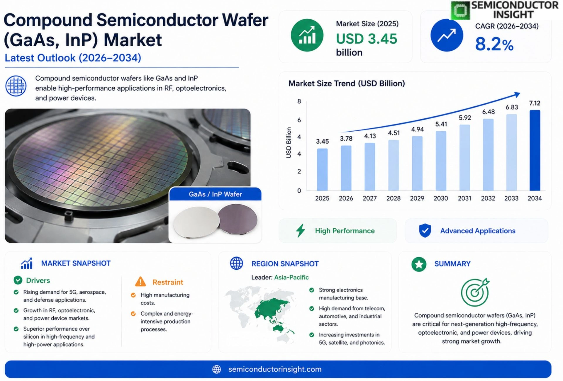
Global Compound Semiconductor Wafer (GaAs, InP) Market size was valued at USD 3.45 billion in 2025. The market is projected to grow from USD 3.78 billion in 2026 to USD 7.12 billion by 2034, exhibiting a CAGR of 8.2% during the forecast period.
Compound semiconductor wafers, primarily composed of gallium arsenide (GaAs) and indium phosphide (InP), are advanced materials engineered for high-frequency, high-power, and optoelectronic applications. These wafers exhibit superior electron mobility and direct bandgap properties compared to silicon, making them indispensable in 5G infrastructure, satellite communications, fiber optics, and high-efficiency photovoltaics. GaAs wafers dominate applications requiring low noise and high-speed performance, such as RF amplifiers and microwave devices, while InP wafers excel in laser diodes, photodetectors, and long-haul optical networks due to their exceptional light-emitting capabilities.
The market is driven by escalating demand for high-performance computing (HPC), electric vehicles (EVs), and renewable energy systems, alongside rapid advancements in wireless communication technologies. Furthermore, the proliferation of IoT devices and the expansion of data centers necessitate energy-efficient components, reinforcing the adoption of compound semiconductors. Strategic collaborations among industry leaders,such as Sumitomo Electric Industries’ expansion of InP wafer production in 2023,are accelerating innovation while addressing supply chain constraints. Key players including Freiberger Compound Materials GmbH, AXT Inc., and IQE plc continue to invest in R&D to enhance wafer purity and scalability, ensuring sustained market growth.
MARKET DRIVERS
Surge in 5G and Wi-Fi 7 Infrastructure
Compound Semiconductor Wafer (GaAs, InP) Market is fundamentally driven by the global mandate for high-speed data transmission and enhanced connectivity. As telecommunications providers upgrade networks to support 5G and future Wi-Fi 7 standards, the demand for RF components utilizing gallium arsenide and indium phosphide wafers has increased significantly.
Growth in Satellite and Aerospace Applications
Indium phosphide wafers are increasingly critical in satellite communications and high-altitude platforms due to their superior thermal stability and high-frequency performance compared to standard silicon.
➤ Increased adoption of Photonic Integrated Circuits (PICs) requires specialized InP wafers for high-density packaging.
Furthermore, the military and aerospace sectors continue to invest heavily in advanced radar and electronic warfare systems, creating a steady demand for high-quality compound semiconductors.
MARKET CHALLENGES
Elevated Raw Material and Process Costs
Manufacturing Compound Semiconductor Wafer (GaAs, InP) Market solutions involves complex epitaxial growth methods like Molecular Beam Epitaxy (MBE) and Metal-Organic Chemical Vapor Deposition (MOCVD). These processes are energy-intensive and require specialized facilities.
Other Challenges
Supply Chain Volatility
Geopolitical tensions and limited mining capabilities for raw materials like gallium and indium can disrupt the consistent supply of substrates needed for mass production.
MARKET RESTRAINTS
Limited Economies of Scale
Unlike the mature silicon semiconductor industry, the market for compound semiconductors operates on a smaller scale globally. This limits the ability to achieve the massive cost reductions associated with silicon wafer manufacturing, making final devices more expensive for end-users.
MARKET OPPORTUNITIES
Optical Interconnects in Data Centers
The rapid expansion of cloud computing and artificial intelligence requires data centers to process vast amounts of information. This creates a significant opportunity for InP-based transceivers that offer higher data rates and lower power consumption compared to copper-based solutions.
Advancement in Automotive Radar Systems
As the automotive industry moves toward Level 3 and Level 4 autonomous driving, the integration of sophisticated radar sensors utilizing GaAs technology becomes essential for safety and navigation.
Trends
Expansion of Wireless and Optical Infrastructure
Market analysts observe a robust trajectory in the industry driven by the rapid evolution of global network infrastructure. The global landscape is increasingly focused on Compound Semiconductor Wafer (GaAs, InP) Market as stakeholders seek materials capable of handling high-frequency signals and high-power demands. Experts note that gallium arsenide and indium phosphide provide distinct advantages over conventional silicon, particularly in optoelectronic environments. Because these materials feature superior electron mobility and direct bandgap properties, they provide the necessary performance levels for modern telecommunications and smart grid initiatives. This technical superiority enables the development of reliable systems essential for 5G infrastructure and satellite communication.
Other Trends
Specialized Material Utilization
Tech professionals are deploying specific wafer types based on rigorous application requirements. Gallium arsenide remains the standard for complex applications necessitating low noise and high-power density, such as microwave devices and radar systems. Conversely, indium phosphide wafers gain significant traction in optical applications where light emission is critical, particularly in laser diodes and high-speed photodetectors used in long-haul fiber optic backbones.
Influence of Electric Mobility and Green Technology
Market researchers identify a significant shift towards energy-efficient systems involving renewable energy and electric vehicle platforms. As data centers expand to support machine learning and internet of things ecosystems, the demand for advanced computing components grows. Key industry players are actively adjusting supply chains to support this transition, ensuring that Compound Semiconductor Wafer (GaAs, InP) Market continues to meet the rigorous technical standards of high-efficiency photovoltaics and high-performance computing hardware.
COMPETITIVE LANDSCAPE
Key Industry Players
Leading Global Suppliers and Innovators in GaAs and InP Wafer Production
The global Compound Semiconductor Wafer Market is characterized by a robust and fragmented competitive structure driven by the escalating demand for high-frequency RF components essential for next-generation wireless infrastructure and satellite systems. Key industry players are heavily investing in advanced epitaxial growth technologies, such as metal-organic chemical vapor deposition (MOCVD) and molecular beam epitaxy (MBE), to meet the rigorous performance standards required for 5G infrastructure and hyperscale data centers. Major manufacturers are significantly expanding their production capacities for both 200mm and 300mm wafers to ensure a stable supply chain for original equipment manufacturers, with a distinct focus on enhancing electron mobility and direct bandgap properties compared to silicon substrates.
In addition to established public companies, the landscape includes specialized privately held firms focusing on niche applications such as high-power optics and photovoltaics. The competitive dynamics are increasingly centered on R&D innovation, with leading firms prioritizing defect reduction, specific doping, and lattice-matched buffer solutions to enhance wafer yield rates. Strategic collaborations and joint ventures are also prevalent as companies seek to integrate vertically and address the complex supply bottlenecks associated with raw material availability. Furthermore, the expansion of electric vehicle markets requires specialized compound materials, prompting aggressive capacity building by market leaders to capture this emerging industrial segment.
List of Key Compound Semiconductor Wafer Companies Profiled
- Sumitomo Electric Industries
- IQE plc
- Freiberger Compound Materials GmbH
- AXT Inc.
- III-V Monolayers
- JENNSA Technology
- DOWA HSM Co., Ltd.
- Shinko Electric Industries
- Sumco Corporation
- Global Catalyst Solutions
- Nokia Solutions and Networks (NSN)
- JX Nippon Mining & Metals
- Welch Allyn (part of OPNE Group)
- Qorvo Inc.
- Kokusai Electric Company
Segment Analysis:
| Segment Category | Sub-Segments | Key Insights |
| By Type |
|
Leading Segment: Gallium Arsenide (GaAs) which utilizes superior electron mobility for robust performance. In contrast, InP wafers excel due to exceptional thermal conductivity and direct bandgap properties, making them indispensable for high-frequency and optoelectronic niches. The market is driven by the necessity for materials that can withstand high-frequency operations without signal loss, creating a dual-track competitive landscape. |
| By Application |
|
Leading Segment: Communications specifically driven by the global expansion of 5G networks. There is a robust demand for energy-efficient components that facilitate high-speed data transport and energy-efficient photovoltaics. The proliferation of IoT devices further reinforces the adoption of compound semiconductors, enabling smaller, faster, and more power-friendly devices compared to silicon alternatives, which is critical for next-generation consumer electronics. |
| By End User |
|
Leading Segment: Telecommunications and Automotive sectors are key drivers of end-user demand. Telecommunications companies are aggressively investing in network upgrades to support high data throughput via satellite communications and fiber optics. Meanwhile, electric vehicle manufacturers are integrating advanced semiconductor solutions to enhance battery management and infotainment efficiency, highlighting a strong alignment between market trends and end-user technical requirements for reliability. |
| By Wafer Material |
|
Leading Segment: Material Differentiation plays a pivotal role in determining application viability. There is a distinct trend towards InP adoption in long-haul optical networks due to its superior light emission capabilities and suitability for laser diodes. Strategic collaborations among industry leaders are accelerating innovation in wafer purity and scalability, addressing supply chain constraints while ensuring sustained market growth across diverse technological tiers. |
| By Performance Tier |
|
Leading Segment: High-Performance Computing and Optoelectronics. Qualitative analysis indicates a bifurcation in the market between mainstream cost-effective solutions and premium, military-grade reliability tiers. Key players continue to invest in R&D to enhance thermal stability and power efficiency, ensuring these advanced materials remain indispensable for emerging applications requiring high operational performance under extreme conditions. |
Regional Analysis: Compound Semiconductor Wafer (GaAs, InP) Market
North American research initiatives prioritize the maturity of InP wafers for photonics and high-frequency applications, fostering a competitive advantage in next-generation communication systems.
The regional shift towards autonomous driving is increasing the demand for compound semiconductor devices capable of supporting safety-critical Advanced Driver-Assistance Systems (ADAS).
Significant capital deployment for 5G backhaul and macro-scale networks is driving the market volume of GaAs-based RF components, ensuring high-speed connectivity across urban and suburban areas.
Localized manufacturing initiatives are reducing dependencies on foreign supply chains, allowing for better control over quality standards and rapid prototyping for defense and commercial sectors.
Europe
Europe’s trajectory Compound Semiconductor Wafer (GaAs, InP) Market is heavily steered by its automotive industry and stringent energy efficiency policies. The region is a global hub for automotive manufacturing, where the integration of compound semiconductors in vehicle electronics is becoming mandatory due to regulations aimed at reducing carbon emissions. Germany and the Nordic countries lead in this domain, utilizing GaAs-based power amplifiers to enhance the efficiency of wireless charging and infotainment systems. Beyond automotive, Europe is witnessing steady growth in the telecommunications sector, with focus on network densification to support IoT ecosystems. The region’s regulatory bodies also encourage research into energy-efficient optoelectronic devices, boosting the relevance of InP wafers in smart grid technologies and optical communication networks. The market dynamics in Europe reflect a cautious yet strategic approach to adoption, prioritizing reliability and long-term sustainability over rapid volume expansion.
Asia-Pacific
Asia-Pacific dominates the manufacturing landscape of Compound Semiconductor Wafer (GaAs, InP) Market, characterized by cost-efficient production capabilities and massive economies of scale. The region is home to the world’s largest consumer electronics manufacturers, driving the ubiquitous demand for GaAs-based mobile device components such as power amplifiers and RF switches. Market leaders in countries like Taiwan, China, and South Korea are aggressively expanding their wafer fabrication capacities to meet the escalating requirements of the 5G and 6G transition. Additionally, the proliferation of data centers in the region is fueling the need for advanced optical interconnects, thereby boosting the InP wafer market. The pace of market expansion here is unmatched globally, supported by favorable government policies that promote semiconductor fabrication infrastructure. This region’s strength lies in its ability to produce volumes at competitive prices, which positions it as the most critical manufacturing hub for the global supply chain.
South America
The South American market for Compound Semiconductor Wafer (GaAs, InP) Market is emerging as a promising frontier, primarily driven by attempts to bridge the digital divide through enhanced telecommunications infrastructure. With a growing middle class and increasing mobile penetration, the region is aggressively pursuing the rollout of 4G and 5G networks, which necessitates the deployment of cost-effective RF components. However, challenges regarding infrastructure stability and supply chain logistics persist. The primary application areas currently revolve around mobile broadband and satellite communications, which are vital for connecting remote agricultural and mining sectors. As urbanization accelerates, the demand for consumer electronics with integrated compound semiconductor components is expected to rise, gradually integrating South America into the broader global value chain of advanced materials.
Middle East & Africa
The Middle East and Africa region is leveraging Compound Semiconductor Wafer (GaAs, InP) Market development for strategic infrastructure projects, particularly in smart city initiatives and defense capabilities. Nations in the Gulf Cooperation Council are investing heavily in digital transformation projects that require high-reliability communication systems, thus creating a niche demand for high-performance RF and microwave components. Furthermore, the security concerns across various nations in the region have escalated the reliance on defense electronics that utilize GaAs technology for signal processing and secure communications. While the market volume is currently smaller compared to the Asian and North American giants, the growth potential is substantial, driven by massive public spending on modernization and technological sovereignty programs aimed at reducing reliance on external technology providers.
Report Scope
This market research report provides a comprehensive analysis of the Compound Semiconductor Wafer (GaAs, InP) Market , covering the forecast period 2026–2034. It offers detailed insights into market dynamics, technological advancements, competitive landscape, and key trends shaping the industry.
Key focus areas of the report include:
- Market Overview: The report begins with an overview outlining its current market scenario, key growth indicators, and industry transformation drivers. It discusses macroeconomic factors, demand–supply balance, regulatory landscape, and the strategic role of semiconductors in powering advancements across industries such as automotive, telecommunications, consumer electronics, and industrial automation.
- Market Size & Forecast: Historical data and future projections for revenue, unit shipments, and market value across major regions and segments.
- Segmentation Analysis: Detailed breakdown by product type, technology, application, and end-user industry to identify high-growth segments and investment opportunities.
- Regional Insights: Insights into market performance across North America, Europe, Asia-Pacific, Latin America, and the Middle East & Africa, including country-level analysis where relevant.
- Competitive Landscape: Profiles of leading market participants, including their product offerings, R&D focus, manufacturing capacity, pricing strategies, and recent developments such as mergers, acquisitions, and partnerships.
- Technology Trends & Innovation: Assessment of emerging technologies, integration of AI/IoT, semiconductor design trends, fabrication techniques, and evolving industry standards.
- Market Drivers & Restraints: Evaluation of factors driving market growth along with challenges, supply chain constraints, regulatory issues, and market-entry barriers.
- Stakeholder Insights: Insights for component suppliers, OEMs, system integrators, investors, and policymakers regarding the evolving ecosystem and strategic opportunities.
Primary and secondary research methods are employed, including interviews with industry experts, data from verified sources, and real-time market intelligence to ensure the accuracy and reliability of the insights presented.
FREQUENTLY ASKED QUESTIONS:
What is the current market size of Compound Semiconductor Wafer (GaAs, InP) Market?
-> Global Compound Semiconductor Wafer (GaAs, InP) Market size was valued at USD 3.45 billion in 2025. The market is projected to grow from USD 3.78 billion in 2026 to USD 7.12 billion by 2034, exhibiting a CAGR of 8.2% during the forecast period.
Which key companies operate Compound Semiconductor Wafer (GaAs, InP) Market?
-> Key players include Sumitomo Electric Industries, Freiberger Compound Materials GmbH, AXT Inc., and IQE plc, among others.
What are the key growth drivers?
-> Key growth drivers include 5G infrastructure, electric vehicles, IoT devices, data centers, renewable energy systems, and high-performance computing.
What are the key materials used?
-> The market is driven by the demand for Gallium Arsenide (GaAs) and Indium Phosphide (InP) wafers due to their superior electron mobility and direct bandgap properties.
What is the market forecast?
-> The market is projected to grow from USD 3.78 billion in 2026 to USD 7.12 billion by 2034, exhibiting aCAGR of 8.2% during the forecast period.

Get Sample Report PDF for Exclusive Insights
Report Sample Includes
- Table of Contents
- List of Tables & Figures
- Charts, Research Methodology, and more...
 Download Sample Report PDF


