
CIS (Image Sensor) Stacked Die Market Insights
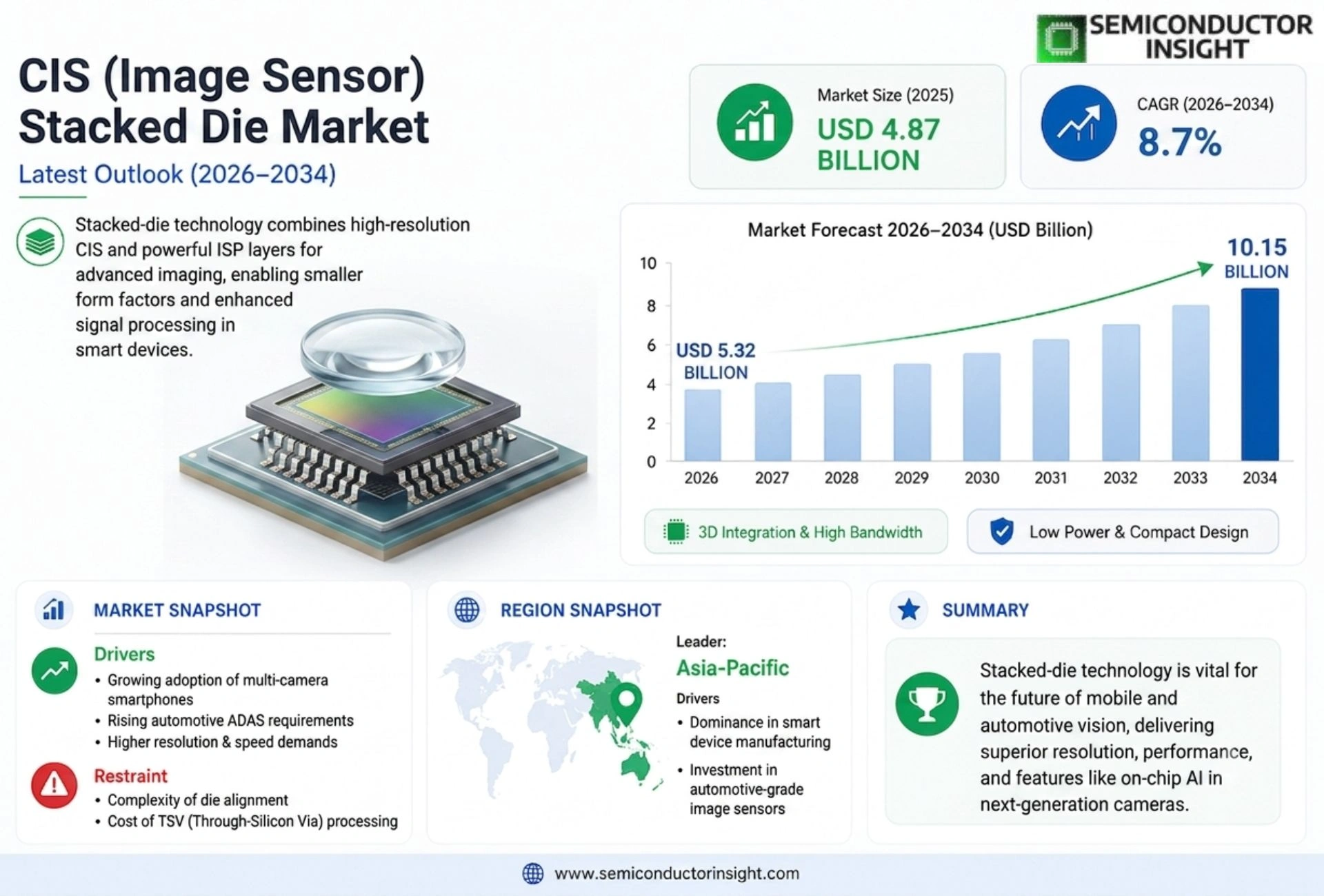
CIS (Image Sensor) Stacked Die Market size was valued at USD 4.87 billion in 2025. The market is projected to grow from USD 5.32 billion in 2026 to USD 10.15 billion by 2034, exhibiting a CAGR of 8.7% during the forecast period.
CIS (Image Sensor) stacked die refers to advanced semiconductor architectures where the pixel array and logic circuitry are fabricated on separate silicon wafers and vertically integrated through hybrid bonding or through-silicon vias (TSVs). This configuration enhances performance, reduces power consumption, and enables higher resolution in compact form factors,critical for applications in smartphones, automotive ADAS, medical imaging, and industrial vision systems. The technology supports backside illumination (BSI), deep trench isolation (DTI), and improved signal-to-noise ratios, making it indispensable for high-speed imaging and computational photography.
The rapid adoption of CIS (Image Sensor) stacked die is driven by escalating demand for high-resolution cameras in consumer electronics, particularly flagship smartphones requiring multi-camera setups with periscope lenses and LiDAR sensors. Furthermore, advancements in autonomous vehicle technologies are accelerating integration into automotive safety systems such as surround-view cameras and driver monitoring systems. Industry leaders like Sony Semiconductor Solutions Corporation, Samsung Electronics Co., Ltd., and OmniVision Technologies continue to innovate with stacked architectures supporting global shutter functionality and AI-enhanced image processing,further propelling market expansion across global markets.
MARKET DRIVERS
Push for Ultra-High Pixel Density
The rapid evolution of mobile communication devices has intensified the demand for image sensors capable of capturing more detail. CIS (Image Sensor) Stacked Die Market is primarily driven by the industry’s shift towards 200-megapixel and higher resolution sensors. Stacked die technology allows manufacturers to integrate more pixels into a smaller surface area, catering to consumer preferences for high-definition photography and videography in smartphones. This trend significantly boosts market growth.
Enhanced Through-Silicon Via (TSV) Performance
Technological advancements in Through-Silicon Via (TSV) fabrication have enabled faster signal transmission between the image sensor and the logic layer. CIS (Image Sensor) Stacked Die Market benefits immensely from this, as improved TSV capabilities reduce readout noise and increase frame rates. This performance boost is crucial for applications requiring real-time image processing, such as electronic viewfinders and mirrorless cameras.
➤ Stacked die structures reduce module thickness, allowing for slimmer device designs.
Furthermore, the integration of logic cores directly onto the stacked die enables a higher level of on-chip processing efficiency, which further propels the adoption of this technology in the global semiconductor landscape.
MARKET CHALLENGES
Thermal Dissipation Limitations
Despite the benefits, CIS (Image Sensor) Stacked Die Market faces challenges regarding thermal management. Bonding a high-performance logic die on top of the sensor die creates a barrier to heat dissipation. High resolutions and faster processing speeds inevitably generate substantial heat within a compact area, which can degrade image quality and sensor longevity if not managed properly.
Other Challenges
Process Complexity and Yield Rates
The fabrication of stacked die technology involves complex bonding processes, such as wafer-level bonding and micro-bumping. These processes are notoriously difficult to execute at high volumes, leading to lower overall yield rates. Consequently, cost per unit remains a significant hurdle for widespread adoption in cost-sensitive segments of the electronics market.
MARKET RESTRAINTS
High Manufacturing Costs
The implementation of stacked die architectures requires specialized fabrication equipment and rigorous quality control measures, leading to elevated production costs. CIS (Image Sensor) Stacked Die Market is constrained by these high capital expenditures, which can limit the profitability for manufacturers operating with thin margins. Despite the long-term benefits, the initial barrier to entry remains high for smaller vendors.
MARKET OPPORTUNITIES
Expansion in Automotive ADAS
The growing implementation of Advanced Driver-Assistance Systems (ADAS) presents a substantial opportunity for CIS (Image Sensor) Stacked Die Market. Modern vehicles require high dynamic range and high frame rate sensors for features like LiDAR, collision avoidance, and night vision. Stacked die sensors offer the necessary performance and power efficiency for these safety-critical automotive applications.
Growth in IoT and 3D Sensing
The proliferation of Internet of Things (IoT) devices and consumer electronics focused on 3D depth sensing also promises significant growth. Stacked die technology is essential for aligning IR (Infrared) projectors and sensors in Time-of-Flight (ToF) cameras. As smart home devices and gesture-recognition technologies mature, the demand for sophisticated stacked die solutions is expected to surge.
Trends
Adoption of Hybrid Bonding and TSV Technologies
The global landscape is witnessing a paradigm shift driven by the necessity for higher performance and lower power consumption. The primary trend involves the adoption of CIS (Image Sensor) Stacked Die technologies, where logic and pixel architectures are vertically integrated using TSVs and hybrid bonding. This approach addresses the physical limitations of monolithic stacking by allowing distinct silicon wafers to be combined. It is essential for enabling backside illumination and deep trench isolation, which directly elevate signal-to-noise ratios. As end-users demand imaging in progressively smaller form factors, the ability to stack components without increasing optical footprint becomes a defining characteristic of modern high-speed imaging systems.
Other Trends
Integration into Automotive ADAS Systems
There is a robust escalation in demand for imaging solutions within the rapidly evolving automotive sector, specifically for Advanced Driver Assistance Systems. As vehicle manufacturers integrate complex sensor suites for safety, the reliance on stacked die technology to support high-speed cameras and surround-view monitoring has increased significantly. The push for autonomous safety features necessitates components that maintain precision across various lighting conditions. Therefore, the development of robust stacked architectures that facilitate seamless sensor fusion becomes a critical priority for ensuring reliable vehicle operation in diverse environments.
Computational Photography in Consumer Electronics
The ubiquity of high-performance cameras in modern smartphones acts as the primary catalyst for market expansion. Contemporary mobile devices are now equipped with sophisticated multi-camera setups designed to handle periscope lenses, LiDAR sensors, and advanced image processing. Major semiconductor leaders are actively engineering solutions that support global shutter functionality and AI-enhanced capabilities. This competitive pressure drives the continuous innovation required to meet the rigorous standards of the global consumer electronics market, ensuring that image quality keeps pace with evolving consumer expectations for visual perfection.
COMPETITIVE LANDSCAPE
Key Industry Players
Global Market Dynamics & Technology Stack
CIS (Image Sensor) Stacked Die Market is witnessing robust growth driven by the widespread adoption of advanced semiconductor architectures that separate pixel arrays from logic circuitry using through-silicon vias (TSVs). This vertical integration allows for enhanced performance and reduced power consumption, catering to the escalating demand for high-resolution imaging in compact form factors for smartphones and automotive applications. Industry analysts note that the adoption of backside illumination and hybrid bonding technologies is critical for supporting next-generation sensor requirements.
Significant investments are flowing into research and development to support global shutter functionality and AI-enhanced image processing, positioning major market leaders to capitalize on the forecasted Compound Annual Growth Rate (CAGR). The competitive landscape is characterized by continuous innovation in computational photography and deep trench isolation methods to improve signal-to-noise ratios for complex industrial and medical imaging systems.
List of Key [Industry] Companies Profiled
- Sony Semiconductor Solutions Corporation
- Samsung Electronics Co., Ltd.
- SK Hynix Inc.
- OmniVision Technologies
- Canon Inc.
- ON Semiconductor
- STMicroelectronics
- Panasonic Corporation
- Teledyne Technologies
- Infineon Technologies
- Micron Technology
- Xiaomi Corporation
- Huawei Technologies Co., Ltd.
Segment Analysis:
| Segment Category | Sub-Segments | Key Insights |
| By Type |
|
Hybrid Bonding Technology is driving the highest growth due to its ability to facilitate high-density interconnects which are essential for stacking logic layers directly onto image sensor dies. This configuration significantly reduces parasitic capacitance and improves overall signal integrity, making it the preferred choice for high-performance computational photography applications. By eliminating the need for complex wire bonding, this specific type enables higher pixel counts and faster communication speeds that are critical for modern flagship devices.
The adoption of TSV technology is prevalent in applications requiring deep vertical integration, allowing for the efficient transmission of electrical signals through multiple layers of silicon. This results in a compact form factor which maximizes the active pixel array area while minimizing chip size, a crucial factor for high-resolution sensors used in medical borescopes and industrial microscopy systems. Ultimately, these advanced structural types enhance power efficiency and support stringent requirements for high-speed imaging in edge computing environments. |
| By Application |
|
Consumer Electronics remains the primary catalyst for market expansion, particularly driven by the relentless demand for multi-camera setups with periscope and telephoto lenses in high-end smartphones. The integration of advanced stacked die architectures allows manufacturers to support backside illumination and deep trench isolation, which are vital for achieving superior low-light performance and computational photography features without increasing the physical bulk of the device. This segment heavily favors solutions that offer high-resolution capturing capabilities essential for augmented reality and virtual reality integration.
Automotive ADAS is an emerging high-value segment defined by the need for robust, high-precision vision systems required for safety features like surround-view monitors and driver monitoring systems. The transition towards autonomous mobility necessitates sensors that can execute complex on-chip processing to reduce latency. Consequently, suppliers are focusing heavily on vertical integration to ensure these advanced image sensors can withstand harsh environmental conditions while delivering high frame rates critical for real-time object detection and path planning. |
| By End User |
|
Smartphone Manufacturers are the dominant end users actively lobbying for further innovation in stacked die technologies to differentiate their product offerings in a intensely competitive market. Their focus is on incorporating more sophisticated sensors that support AI-driven image processing and 3D sensing capabilities. This end user segment demands high yield rates and cost efficiency, pushing suppliers to adopt advanced packaging solutions that streamline production cycles and ensure reliability during high-volume manufacturing outputs.
For Automotive OEMs and Medical Device OEMs, the primary strategic imperative is reliability and performance consistency across varying operational conditions. These industries require sensors that offer exceptional signal-to-noise ratios and can operate efficiently in diverse thermal and mechanical environments. The strategic partnership between these end users and semiconductor suppliers is increasingly focused on co-engineering custom stacked die solutions that optimize specific imaging workflows, such as low-dose radiation imaging or high-speed machine vision inspection, ensuring the final systems meet rigorous industry standards and regulatory compliance requirements. |
| By Packaging Process |
|
Silicon Interposer Technology plays a pivotal role in facilitating the vertical stacking of image sensors by providing a dense and precise electrical pathway between separate wafers. This packaging method is widely utilized to manage thermal dissipation, which is a critical challenge when tightly packing high-performance computing logic with image sensors. By isolating the two distinct functional areas, manufacturers can optimize signal integrity and reduce crosstalk, leading to higher overall image quality and more stable performance during prolonged operation. This process is particularly favored in applications where mechanical stability and precise alignment are non-negotiable. |
| By Functional Feature |
|
On-Chip Image Signal Processing is rapidly becoming a standard feature that transforms the image sensor from a passive light-capturing component into an active intelligent node. By embedding processing logic directly onto the sensor die, manufacturers can offload significant computational tasks such as noise reduction and facial recognition directly at the source, thereby drastically reducing the power consumption required for image transmission. This functionality is essential for real-time video streaming and autonomous decision-making in industrial robotics, where minimizing latency is crucial for system speed and safety. |
Regional Analysis: CIS (Image Sensor) Stacked Die Market
Asia-Pacific
The proliferation of mobile devices featuring multiple rear cameras has accelerated the need for sophisticated stacked die architectures. Manufacturers are adopting these advanced packaging techniques to house memory and logic within the same physical stack, thereby improving signal-to-noise ratios and enabling higher megapixel counts without compromising the device’s physical footprint or battery efficiency.
Autonomous driving initiatives are fueling a significant strategic shift toward the integration of high-definition, stack-based sensors in vehicle systems. The demand for superior depth sensing and low-light performance in automotive environments creates a unique niche withCIS (Image Sensor) Stacked Die Market, driving innovation in how multiple sensor layers are integrated to support driver-assistance functionalities.
As the industry moves beyond traditional 2D lithography, businesses are actively pursuing 2.5D and 3D stacking as viable strategies to enhance device performance. This transition allows for closer proximity between the image sensor and other essential components, significantly reducing latency and power consumption while maintaining high levels of integration for complex imaging tasks.
Beyond mobile phones, the adoption of stack-based sensors has expanded rapidly into the realm of Augmented Reality (AR) and Virtual Reality (VR). These immersive technologies require sensors that can capture wide fields of view and high dynamic range, necessitating specialized vertical integration strategies that cater specifically to the spatial computing sector’s emerging business landscape.
North America
North America maintains a pivotal position CIS (Image Sensor) Stacked Die Market, largely driven by the region’s strong focus on research and development alongside a robust consumer electronics sector. The United States serves as a hub for technological innovation, often leading trends in computational photography and high-end industrial imaging applications. Strategic partnerships between local electronics firms and global semiconductor manufacturers ensure that premium tiers of stacked die products are readily available, catering to a market that values image quality and performance above all else.
Europe
Europe represents a critical and growing segment for CIS (Image Sensor) Stacked Die Market, specifically through its influence on the automotive and industrial automation sectors. The region’s adherence to strict environmental and safety regulations has accelerated the adoption of sophisticated in-vehicle visual systems, including surround-view and night-vision applications. Key automotive suppliers in the area are increasingly relying on advanced sensor stacking technologies to meet the complex requirements of modern electric vehicles and autonomous driving platforms.
South America
South America is currently experiencing a gradual yet steady expansion withCIS (Image Sensor) Stacked Die Market, characterized by increasing penetration of mobile technology across diverse economic strata. As the region’s middle class expands, the demand for affordable devices equipped with multi-camera setups is driving manufacturers to optimize stack die processes for cost-effective production without sacrificing essential imaging quality.
Middle East & Africa
The Middle East & Africa region offers significant development opportunities for market players seeking to establish a foothold in emerging economies. Large-scale infrastructure projects focused on smart cities and digital transformation are creating a growing ecosystem for surveillance, security, and public transportation systems that utilize high-capacity imaging solutions, thereby supporting the broader adoption of advanced photonic technologies.
Report Scope
This market research report provides a comprehensive analysis of the CIS (Image Sensor) Stacked Die Market , covering the forecast period 2026–2034. It offers detailed insights into market dynamics, technological advancements, competitive landscape, and key trends shaping the industry.
Key focus areas of the report include:
- Market Overview: The report begins with an overview outlining its current market scenario, key growth indicators, and industry transformation drivers. It discusses macroeconomic factors, demand–supply balance, regulatory landscape, and the strategic role of semiconductors in powering advancements across industries such as automotive, telecommunications, consumer electronics, and industrial automation.
- Market Size & Forecast: Historical data and future projections for revenue, unit shipments, and market value across major regions and segments.
- Segmentation Analysis: Detailed breakdown by product type, technology, application, and end-user industry to identify high-growth segments and investment opportunities.
- Regional Insights: Insights into market performance across North America, Europe, Asia-Pacific, Latin America, and the Middle East & Africa, including country-level analysis where relevant.
- Competitive Landscape: Profiles of leading market participants, including their product offerings, R&D focus, manufacturing capacity, pricing strategies, and recent developments such as mergers, acquisitions, and partnerships.
- Technology Trends & Innovation: Assessment of emerging technologies, integration of AI/IoT, semiconductor design trends, fabrication techniques, and evolving industry standards.
- Market Drivers & Restraints: Evaluation of factors driving market growth along with challenges, supply chain constraints, regulatory issues, and market-entry barriers.
- Stakeholder Insights: Insights for component suppliers, OEMs, system integrators, investors, and policymakers regarding the evolving ecosystem and strategic opportunities.
Primary and secondary research methods are employed, including interviews with industry experts, data from verified sources, and real-time market intelligence to ensure the accuracy and reliability of the insights presented.
FREQUENTLY ASKED QUESTIONS:
What is the current market size of CIS (Image Sensor) Stacked Die Market?
-> CIS (Image Sensor) Stacked Die Market size was valued at USD 4.87 billion in 2025. The market is projected to grow from USD 5.32 billion in 2026 to USD 10.15 billion by 2034, exhibiting a CAGR of 8.7% during the forecast period.
Which key companies operate CIS (Image Sensor) Stacked Die Market?
-> Key players include Sony Semiconductor Solutions Corporation, Samsung Electronics Co., Ltd., and OmniVision Technologies, among others.
What are the key growth drivers?
-> Key growth drivers include escalating demand for high-resolution cameras in consumer electronics, particularly smartphones, and advancements in automotive ADAS technologies.
Which region dominates the market?
-> Asia-Pacific is a dominant market, while global markets witness significant expansion.
What are the emerging trends?
-> Emerging trends include stacked architectures supporting global shutter functionality and AI-enhanced image processing.

Get Sample Report PDF for Exclusive Insights
Report Sample Includes
- Table of Contents
- List of Tables & Figures
- Charts, Research Methodology, and more...
 Download Sample Report PDF

