
Chemical Mechanical Planarization (CMP) Pads Market Insights
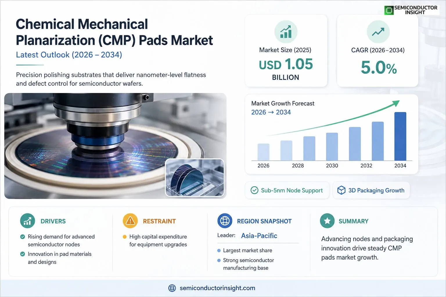
Global CMP pads market size was valued at USD 1.05 billion in 2025. The market is projected to grow from USD 1.12 billion in 2026 to USD 1.68 billion by 2034, exhibiting a CAGR of 5.0% during the forecast period.
Chemical Mechanical Planarization (CMP) pads are precision‑engineered polishing substrates used in semiconductor wafer planarization to achieve nanometer‑level flatness and defect control. They consist of a polymeric backing layer impregnated with abrasive particles such as silica or diamond, and are designed to balance removal rate, surface uniformity, and pad wear for advanced node manufacturing.
The market is experiencing rapid growth due to several factors, including increased investment in semiconductor fabrication, rising demand for advanced logic and memory chips, and the push toward sub‑5 nm process technologies. Furthermore, the adoption of high‑density interconnects and three‑dimensional packaging drives higher consumption of CMP consumables. Initiatives by key players such as Cabot Microelectronics, Dow Chemical, and Applied Materials,who continuously innovate pad formulations and surface treatments,are expected to sustain momentum.
MARKET DRIVERS
Rising Demand for Advanced Semiconductor Nodes
Chemical Mechanical Planarization (CMP) Pads Market is being propelled by the semiconductor industry’s shift toward sub‑10 nm nodes, which require highly uniform wafer surfaces. manufacturers are investing heavily in CMP pads that deliver lower defectivity and improved planarity, thereby sustaining growth in the sector.
Innovation in Pad Materials and Designs
Recent breakthroughs in nanocomposite polishing pads and slurry‑compatible chemistries have enhanced removal rates while preserving wafer integrity. Companies that integrate these innovations are seeing higher yield and shorter cycle times, reinforcing market expansion.
➤ “Adoption of next‑generation CMP pads is expected to accelerate as fabs aim for 3‑5 % cost reductions per wafer.”
Additionally, the growth of emerging applications such as 5G, AI accelerators, and automotive electronics is driving greater investment in CMP tooling, further cementing the market’s upward trajectory.
MARKET CHALLENGES
Stringent Defect Control Requirements
Although demand is strong, fabs must meet exceptionally low defect thresholds. Even minor contamination from CMP pads can lead to yield losses, compelling manufacturers to adopt rigorous quality‑control protocols that increase operational complexity.
Other Challenges
Environmental Compliance
Regulatory pressure to reduce hazardous waste from polishing slurries forces suppliers to develop eco‑friendly pad formulations, adding R&D costs and potentially slowing product roll‑out.
MARKET RESTRAINTS
High Capital Expenditure for Upgrades
Upgrading existing CMP lines to accommodate newer pad technologies often demands substantial capital investment. Smaller fabs, in particular, may delay adoption, creating a restraint on overall market penetration.
MARKET OPPORTUNITIES
Growth in Specialized Packaging and 3D Integration
The rise of advanced packaging formats such as Fan‑Out Wafer Level Packaging (FO‑WLP) and 3D‑IC stacking opens new opportunities for Chemical Mechanical Planarization (CMP) Pads Market. Tailored pad solutions that address the unique planarization challenges of these technologies are expected to attract significant investment from leading semiconductor manufacturers.
Chemical Mechanical Planarization (CMP) Pads Market Trends
Growth Driven by Sub‑5 nm Node Advancement
Chemical Mechanical Planarization (CMP) Pads Market is responding to intensified pressure from semiconductor manufacturers to support sub‑5 nm process nodes. As chipmakers pursue tighter critical dimensions, the need for planarization substrates that can reliably achieve nanometer‑level flatness while minimizing defect generation has risen sharply. Leading suppliers are refining pad formulations to balance removal rate with surface uniformity, enabling higher yield during advanced node production. This shift is reflected in increased procurement volumes across fabs focused on high‑performance logic and memory devices.
Other Trends
Shift Toward High‑Density Interconnects and 3D Packaging
High‑density interconnect (HDI) structures and three‑dimensional (3D) packaging architectures are becoming mainstream as they allow greater functional integration per wafer. The CMP Pads Market is seeing greater consumption of consumables that can maintain planarity across uneven topographies inherent to HDI and 3D stacks. Pad manufacturers are therefore engineering surface‑treatment technologies that improve abrasion consistency on both planar and non‑planar features, supporting the reliability demands of these emerging package formats.
Material Innovation and Sustainability Focus
Material innovation remains a pivotal trend. Companies are exploring polymer‑backed pads with hybrid abrasive particles, such as silica‑diamond blends, to extend pad life while delivering higher removal efficiency. Concurrently, sustainability initiatives are prompting the development of pads with reduced waste and recyclable backing layers. These efforts aim to lower the overall cost of ownership for fabs and align with broader environmental goals without sacrificing performance.
COMPETITIVE LANDSCAPEKey Industry Players
CMP Pads Market – Competitive Landscape Overview
Chemical Mechanical Planarization (CMP) Pads Market is currently led by a handful of large multinational corporations that combine deep semiconductor expertise with advanced materials science. Cabot Microelectronics, Dow Chemical, and Applied Materials together command the majority of global CMP pad shipments, leveraging proprietary slurry‑pad chemistries and high‑throughput manufacturing lines to serve leading foundries. Their extensive R&D pipelines focus on ultra‑low defect pads for sub‑5 nm nodes, positioning these firms as the primary drivers of the market’s projected CAGR of 5 % through 2034. The concentration of sales around these three players creates a tiered supply chain where smaller distributors source pads from the major manufacturers before reaching semiconductor fabs.
Beyond the dominant trio, a diverse set of niche and regional suppliers enriches the competitive landscape. Companies such as 3M, Fujifilm, Entegris, Mitsui Chemicals, and Tokyo Electron offer specialized pad formats tailored for high‑density interconnect and 3‑D packaging applications. Emerging innovators like Planar Systems, NOVACentrix, and Lithoz focus on next‑generation abrasive technologies, while established equipment makers including Nikon, Hitachi High‑Technologies, and Veeco Instruments integrate CMP pad solutions into broader process tooling portfolios. These players collectively enhance product differentiation and sustain healthy market dynamics despite the overall concentration among the top three manufacturers.
List of Key CMP Pads Market Companies Profiled
- Cabot Microelectronics
- Dow Chemical
- Applied Materials
- 3M
- Fujifilm
- Entegris
- Mitsui Chemicals
- Tokyo Electron
- Planar Systems
- TOK
- NOVACentrix
- Nikon
- Hitachi High‑Technologies
- Lithoz
- Veeco Instruments
Segment Analysis:
| Segment Category | Sub-Segments | Key Insights |
| By Type |
|
Soft Pads are increasingly preferred for advanced node planarization because:
|
| By Application |
|
Advanced Packaging drives the most nuanced pad requirements:
|
| By End User |
|
Semiconductor Foundries dominate consumption because:
|
| By Material |
|
Silica‑based Pads remain the core choice for most processes:
|
| By Process Stage |
|
Pre‑Polish Conditioning is critical for ensuring pad readiness:
|
Regional Analysis: North America
North America
The North American market is at the forefront of technological advancements in CMP pads. Focus is on developing pads for advanced nodes and improving polishing uniformity and defect reduction.
Innovation in pad materials, including hybrid and advanced ceramic formulations, is a key trend in North America, aimed at enhancing performance and addressing emerging challenges.
Increasing emphasis on environmentally friendly and sustainable CMP pad materials and manufacturing processes is evident across North America.
The North American CMP pads market is characterized by a mix of established global players and regional specialists, fostering healthy competition and innovation.
Europe
Europe presents a stable and technologically advanced market for CMP pads. With a strong presence of semiconductor manufacturers in countries like Germany, France, and the Netherlands, the demand for high-performance CMP pads remains consistent. The European market is particularly focused on energy-efficient and environmentally responsible CMP solutions, aligning with the region’s stringent environmental regulations. Research and development efforts in Europe are geared towards developing CMP pads for advanced packaging and heterogeneous integration technologies.
Asia-Pacific
Asia-Pacific is the largest and fastest-growing market for CMP pads globally. The region’s dominance in semiconductor manufacturing, particularly in countries like Taiwan, South Korea, and China, drives significant demand. The rapid expansion of the electronics industry and the increasing adoption of advanced technologies are key factors fueling market growth. Asia-Pacific is witnessing a surge in demand for CMP pads used in the production of memory chips and power semiconductors.
Middle East & Africa
The Middle East & Africa region represents a relatively small but growing market for CMP pads. The expansion of the electronics industry in countries like Saudi Arabia and South Africa, along with government initiatives promoting semiconductor manufacturing, are expected to drive market growth in the coming years. The demand for CMP pads is primarily driven by the increasing production of consumer electronics and automotive electronics.
South America
South America is an emerging market for CMP pads with potential for future growth. The development of the electronics industry in countries like Brazil and Chile, coupled with investments in infrastructure and manufacturing, is expected to drive demand. The initial focus in South America is on CMP pads used in the production of consumer electronics and industrial equipment.
United States
The United States represents a significant segment within the North American CMP pads market, boasting a strong concentration of semiconductor design and manufacturing companies. The demand for advanced CMP solutions is driven by the ongoing development of cutting-edge technologies and the increasing complexity of chip designs. The US market is characterized by a high level of innovation and a focus on developing specialized CMP pads for specific applications.
Report Scope
This market research report provides a comprehensive analysis of the Chemical Mechanical Planarization (CMP) Pads Market , covering the forecast period 2026–2034. It offers detailed insights into market dynamics, technological advancements, competitive landscape, and key trends shaping the industry.
Key focus areas of the report include:
- Market Overview: The report begins with an overview outlining its current market scenario, key growth indicators, and industry transformation drivers. It discusses macroeconomic factors, demand–supply balance, regulatory landscape, and the strategic role of semiconductors in powering advancements across industries such as automotive, telecommunications, consumer electronics, and industrial automation.
- Market Size & Forecast: Historical data and future projections for revenue, unit shipments, and market value across major regions and segments.
- Segmentation Analysis: Detailed breakdown by product type, technology, application, and end-user industry to identify high-growth segments and investment opportunities.
- Regional Insights: Insights into market performance across North America, Europe, Asia-Pacific, Latin America, and the Middle East & Africa, including country-level analysis where relevant.
- Competitive Landscape: Profiles of leading market participants, including their product offerings, R&D focus, manufacturing capacity, pricing strategies, and recent developments such as mergers, acquisitions, and partnerships.
- Technology Trends & Innovation: Assessment of emerging technologies, integration of AI/IoT, semiconductor design trends, fabrication techniques, and evolving industry standards.
- Market Drivers & Restraints: Evaluation of factors driving market growth along with challenges, supply chain constraints, regulatory issues, and market-entry barriers.
- Stakeholder Insights: Insights for component suppliers, OEMs, system integrators, investors, and policymakers regarding the evolving ecosystem and strategic opportunities.
Primary and secondary research methods are employed, including interviews with industry experts, data from verified sources, and real-time market intelligence to ensure the accuracy and reliability of the insights presented.
FREQUENTLY ASKED QUESTIONS:
What is the current market size of Chemical Mechanical Planarization (CMP) Pads Market?
-> Chemical Mechanical Planarization (CMP) Pads Market was valued at USD 1.05 billion in 2025 and is expected to reach USD 1.68 billion by 2034, indicating a CAGR of 5.0% over the forecast period.
Which key companies operate in Chemical Mechanical Planarization (CMP) Pads Market?
-> Key players include Cabot Microelectronics, Dow Chemical, and Applied Materials, among others.
What are the key growth drivers?
-> Key growth drivers include increased investment in semiconductor fabrication, rising demand for advanced logic and memory chips, the transition to sub‑5 nm process technologies, and the adoption of high‑density interconnects and three‑dimensional packaging.
Which region dominates the market?
-> The reference does not specify a dominant region; regional insights are pending further data.
What are the emerging trends?
-> Emerging trends include development of high‑density interconnects, three‑dimensional packaging solutions, and innovative pad formulations to support sub‑5 nm node manufacturing.

Get Sample Report PDF for Exclusive Insights
Report Sample Includes
- Table of Contents
- List of Tables & Figures
- Charts, Research Methodology, and more...
 Download Sample Report PDF


