
Advanced Package Metrology (3D X-ray, SAM) Market Insights
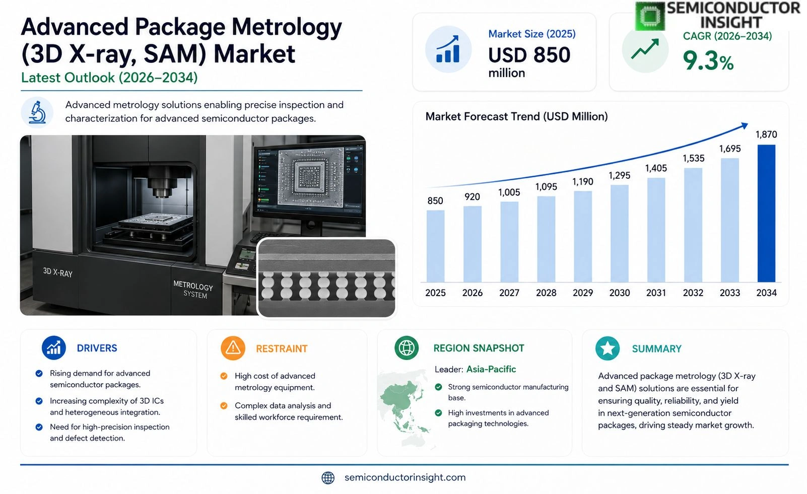
Advanced Package Metrology (3D X-ray, SAM) Market size was valued at USD 850 million in 2025. The market is projected to grow from USD 920 million in 2026 to USD 1.87 billion by 2034, exhibiting a CAGR of 9.3% during the forecast period.
Advanced package metrology, encompassing 3D X-ray inspection and Scanning Acoustic Microscopy (SAM), represents a critical segment of semiconductor manufacturing and quality assurance. These technologies enable non-destructive evaluation of packaged semiconductor devices, detecting defects such as voids, delamination, cracks, and solder joint anomalies with micron-level precision. While 3D X-ray metrology excels in volumetric analysis of internal structures,particularly for flip-chip, wafer-level packaging, and system-in-package (SiP) architectures,SAM specializes in identifying interfacial defects within layered materials through high-frequency ultrasonic waves. Together, they form the backbone of failure analysis and process control in advanced packaging workflows.
The demand for these metrology solutions is intensifying due to the proliferation of heterogeneous integration, miniaturization trends such as chiplet-based designs, and stringent reliability requirements across automotive, aerospace, and consumer electronics sectors. Furthermore, the adoption of AI-driven defect classification and automated inspection systems is enhancing throughput while reducing false positives,key factors driving market expansion among leading equipment providers like KLA Corporation, Nordson DAGE, and Sonoscan.
MARKET DRIVERS
Proliferation of High-Performance Semiconductor Packaging
Advanced Package Metrology (3D X-ray, SAM) Market is primarily propelled by the relentless demand for miniaturization and enhanced functionality in electronic devices. As device geometries continue to shrink, manufacturers face increasing pressure to ensure that every layer of the advanced package is defect-free. This necessitates sophisticated inspection technologies capable of detecting micro-defects that conventional vision systems cannot identify.
Furthermore, the shift towards heterogeneous integration, which aggregates various functions onto a single silicon die, significantly increases the complexity of packaging layers. This complexity drives the adoption of advanced metrology tools like Scanning Acoustic Microscopy (SAM) and 3D X-ray, as they are essential for non-destructive testing of high-density interconnects and embedded components. With the global microelectronics market projected to grow steadily, the reliance on these precise inspection techniques continues to rise.
➤ The transition to more complex 3D packaging architectures is fundamentally altering the quality control landscape.
Additionally, the rigorous reliability standards in automotive and aerospace applications require unparalleled defect detection rates. High-performance computing sectors also contribute to market growth by demanding lower power consumption and higher bandwidth, which are only achievable through advanced packaging techniques that necessitate rigorous metrology verification.
MARKET CHALLENGES
Skill Gap in Technical Personnel
One of the primary hurdles Advanced Package Metrology (3D X-ray, SAM) Market is the scarcity of highly skilled personnel capable of operating and interpreting complex metrology data. These machines are highly sophisticated instruments that require specialized knowledge in signal processing and material science. The rapid technological evolution often outpaces workforce development, creating a bottleneck where the availability of experts does not meet the operational demand of advanced semiconductor fabs.
Other Challenges
High Equipment Maintenance Costs
Calibration and maintenance of 3D X-ray and SAM systems are resource-intensive and can lead to significant downtime if not managed effectively.
Slow Throughput Rates
Analyzing complex 3D packages with high resolution often results in longer inspection times, which can be a bottleneck in high-volume production lines.
MARKET RESTRAINTS
Material Analysis Limitations
Despite the capabilities of Advanced Package Metrology tools, there are inherent limitations regarding material contrast detection. For instance, 3D X-ray systems may struggle to differentiate between low-density materials or specific non-conductive insulators embedded within a metal structure. This limitation can lead to false positives or false negatives in defect detection, complicating the yield management process and potentially delaying time-to-market for new products.
Furthermore, the depth of penetration for 3D X-ray imaging decreases as resolution requirements increase. This trade-off forces manufacturers to balance between seeing deep internal structures clearly and resolving fine surface or near-surface details, often resulting in compromise during the inspection phase.
MARKET OPPORTUNITIES
Automation and AI Integration
Advanced Package Metrology (3D X-ray, SAM) Market presents vast opportunities for growth through the integration of Artificial Intelligence and automated data analysis. By leveraging machine learning algorithms, manufacturers can significantly speed up defect classification and identification processes. This automation reduces the dependency on manual analysis, lowers human error rates, and increases throughput, making advanced metrology accessible to a broader range of production facilities.
Another significant opportunity lies in the expansion of the automotive and Industrial Internet of Things (IIoT) sectors. As these industries move towards safer, more reliable electronics, the demand for robust non-destructive testing is skyrocketing. Providers of metrology solutions can capitalize on this trend by developing specialized inspection protocols tailored to the harsh environmental standards required by these sectors.
Trends
Technological Evolution in Inspection and Quality Assurance
The Advanced Package Metrology (3D X-ray, SAM) sector is witnessing robust expansion driven by the critical need for precision in modern semiconductor fabrication. As the industry moves toward extreme miniaturization and heterogeneous integration, the reliance on non-destructive evaluation of packaged semiconductor devices has become a standard requirement for ensuring operational continuity. This technological evolution allows manufacturers to validate device functionality and process control across a wide range of complex packaging workflows without disrupting the high-volume production environment, establishing a direct correlation between advanced metrology and improved manufacturing yields.
Other Trends
Volumetric Analysis and Interfacial Defect Detection
Manufacturing facilities are increasingly prioritizing sophisticated metrology solutions to perform volumetric analysis of internal structures, particularly for flip-chip and wafer-level packaging configurations. Advanced x-ray and scanning acoustic microscopy technologies specialize in identifying interfacial defects within layered materials through high-frequency ultrasonic waves. By focusing on these critical non-destructive evaluation techniques, engineers can detect hidden anomalies such as voids and delamination with micron-level precision, ensuring that critical reliability requirements are met before final assembly is completed.
Automated Inspection and AI-Driven Reliability
A significant trend in the market is the adoption of automated inspection systems enhanced by AI-driven classification algorithms to significantly streamline the defect detection process. This shift helps leading equipment providers and manufacturing units enhance throughput while minimizing false positives during the analysis of complex semiconductor devices. As industries such as automotive and consumer electronics demand higher consistency and reduced product failure rates, the integration of automated metrology with intelligent analysis tools becomes a strategic necessity for maintaining high standards of product integrity in a competitive global environment.
COMPETITIVE LANDSCAPE
Key Industry Players
Market Analysis & Growth Trends
Advanced Package Metrology (3D X-ray, SAM) Market size was valued at USD 850 million in 2025. The market is projected to grow from USD 920 million in 2026 to USD 1.87 billion by 2034, exhibiting a CAGR of 9.3% during the forecast period. This market encompasses critical 3D X-ray inspection and Scanning Acoustic Microscopy (SAM) solutions, representing a vital segment of semiconductor manufacturing and quality assurance. These technologies enable non-destructive evaluation of packaged devices, detecting defects such as voids, delamination, and solder joint anomalies with micron-level precision.
Market demand intensifies due to heterogeneous integration and miniaturization trends, particularly chiplet-based designs and automotive applications. Advanced package metrology, encompassing 3D X-ray inspection and Scanning Acoustic Microscopy (SAM), represents a critical segment of semiconductor manufacturing and quality assurance. Together, they form the backbone of failure analysis and process control in advanced packaging workflows. Leading equipment providers like KLA Corporation and Nordson DAGE drive the adoption of AI-driven defect classification and automated inspection systems, enhancing throughput while reducing false positives.
List of Key Advanced Package Metrology Companies Profiled
- KLA Corporation
- Nordson DAGE
- Sonoscan
- Hitachi High-Tech
- Varex Imaging
- Nanometrics Incorporated
- Bruker
- Tokyo Electron
- Nikon Metrology
- ULVAC-POLHI
Segment Analysis:
| Segment Category | Sub-Segments | Key Insights |
| By Type |
|
Complementary Technologies drive demand as X-ray solutions excel in volumetric analysis for internal structures like flip-chips while SAM provides superior sensitivity for detecting interfacial adhesive integrity within stacked packages. This segmentation reflects a market preference for integrated systems that combine volumetric density measurements with material bonding checks to ensure System in Package (SiP) reliability. |
| By Application |
|
Compliance and Yield Optimization are the primary drivers in this segment. High volume manufacturing requires rigorous process control to prevent defects from reaching the end market, while failure analysis serves as the critical feedback loop for engineering teams. The shift towards heterogeneous integration necessitates applications that can handle complex multi-layer architectures, making the distinction between pre-silicon process verification and post-packaging validation increasingly relevant. |
| By End User |
|
Demand for High-Reliability Validation varies significantly across foundries and OSATs. Foundries focus on high-volume throughput and standardization, whereas OSATs are focused on custom packaging solutions and the specific reliability requirements of diverse end-user industries. The market shows a growing trend of specialized OSATs investing heavily in advanced metrology capabilities to attract complex customer designs, particularly for edge computing and automotive applications. |
| By Industry Vertical |
|
Stringency of Reliability Standards dictates inspection depth. Consumer electronics demand rapid inspection speeds and cost-effective solutions, whereas automotive and aerospace sectors prioritize microscopic defect detection and extreme environmental stress testing. This vertical segmentation highlights that while technology is universal, the required inspection tolerance and frequency differ drastically based on the intended application environment and safety standards. |
| By Deployment Model |
|
Optimization of Capital Expenditure is the central theme here. Large OEMs with predictable high-volume manufacturing often deploy on-site equipment for continuous process monitoring to maintain throughput. Conversely, smaller design firms and smaller market players tend to utilize service bureaus to access high-end 3D X-ray and SAM capabilities without incurring the high capital costs and maintenance overheads associated with owning and operating these sophisticated inspection platforms. |
Regional Analysis:
North America
The region’s dominance is fueled by demand for connectivity solutions. Innovations in Advanced Package Metrology (3D X-ray, SAM) are critical for verifying the high-density interconnects required in 5G infrastructure and advanced processors, ensuring signal integrity in rapidly evolving hardware ecosystems.
Recent shifts in industrial policy have encouraged localized manufacturing efforts in North America. Metrology plays a pivotal role in these strategies by providing the inspection accuracy needed for domestic production of critical components, thereby securing the regional supply chain for advanced packaging technologies.
The automotive sector in North America is undergoing a digital transformation, driving the need for robust testing solutions. Advanced Package Metrology (3D X-ray, SAM) is essential for validating electronic control units and sensor packages used in next-generation intelligent vehicles, ensuring durability under extreme conditions.
Strong partnerships between semiconductor equipment makers and packaging houses are prevalent. These collaborations Advanced Package Metrology (3D X-ray, SAM) Market foster faster adoption of cutting-edge SAM and X-ray technologies, accelerating the time-to-market for advanced semiconductor products.
Europe
Europe represents a significant portion of the global landscape for Advanced Package Metrology (3D X-ray, SAM) Market, driven by its strong automotive and industrial base. The region is characterized by a focus on energy efficiency and sustainable manufacturing practices. Western European countries are investing heavily in 2.5D and 3D packaging solutions to support the electric vehicle revolution and renewable energy technologies. The regulatory environment emphasizes environmental and worker safety, which favors Non-Destructive Testing methods like 3D X-ray and SAM over destructive testing. Market players in Europe are prioritizing the development of high-precision inspection tools that can handle the specific packaging requirements of automotive-grade chips. The integration of digital twins into the manufacturing process is also influencing the demand for advanced metrology software and hardware. Collaborative research initiatives among universities and technical institutes in Germany and the Netherlands are helping to refine inspection techniques for future semiconductor nodes. The European Advanced Package Metrology (3D X-ray, SAM) Market is set to evolve as the automotive industry moves towards full electrification, requiring more sophisticated electronic control units and sensors that demand rigorous quality control measures to ensure safety and reliability.
Asia-Pacific
The Asia-Pacific region is the powerhouse of manufacturing, serving as a central hub for the global production of semiconductor devices. This region holds a massive share Advanced Package Metrology (3D X-ray, SAM) Market due to the concentration of foundries and fabless companies. The demand for cost-effective and high-volume inspection solutions is exceptionally high, as manufacturers seek to optimize throughput without compromising on yield. Countries like South Korea, Taiwan, and Japan are leaders in advanced packaging techniques, creating a robust pull for specialized metrology tools. The rapid expansion of the consumer electronics sector here directly correlates with the increasing need to inspect complex multilayer packages. As Asian economies prioritize technological self-sufficiency, the local development of metrology infrastructure is accelerating. The focus remains on volume production and the ability to detect faults in high-speed assembly lines. The regional strategy involves leveraging the vast supply chain ecosystem to integrate metrology solutions directly into the packaging lines, ensuring real-time quality feedback. The growth of Advanced Package Metrology (3D X-ray, SAM) Market in Asia-Pacific is expected to remain steady, driven by the continuous push for miniaturization in mobile devices and high-performance computing systems.
South America
South America is an emerging market for Advanced Package Metrology (3D X-ray, SAM) Market, showing promising growth potential as the local semiconductor ecosystem matures. The region’s industries, including mining, agriculture, and communications, are beginning to adopt more advanced packaging solutions to handle demanding environmental conditions. Brazil and Argentina are key contributors to this regional shift, with increasing investments in industrial automation and electronics. The demand for Advanced Package Metrology (3D X-ray, SAM) in South America is largely driven by the need for reliable maintenance and testing of industrial equipment. While the market is still developing compared to other regions, the focus is slowly shifting towards high-tech sectors as the region invests in digital transformation projects. Local manufacturers are increasingly aware of the importance of quality assurance in advanced packaging to compete in global markets. The slow but steady growth Advanced Package Metrology (3D X-ray, SAM) Market in South America reflects the broader economic recovery and industrial upgrading efforts in the region. Stakeholders in this area are looking towards strategic partnerships to import necessary metrology expertise and technologies to boost local production capabilities.
Middle East & Africa
The Middle East & Africa region presents a niche but potential avenue for Advanced Package Metrology (3D X-ray, SAM) Market, primarily driven by infrastructure projects and defense electronics. The market dynamics here are highly influenced by the need for ruggedized electronics capable of withstanding harsh climates. The focus in this region is on ensuring the long-term durability and performance of packaged electronic components used in oil and gas, defense, and smart city projects. The adoption of Advanced Package Metrology (3D X-ray, SAM) is growing as local industries recognize the risks associated with quality failures in critical applications. Investments in the region are increasingly focused on diversifying economies away from raw commodity extraction towards technology and manufacturing. This strategic pivot necessitates a reliable supply chain for inspection technologies. The Middle East & Africa Advanced Package Metrology (3D X-ray, SAM) Market is currently experiencing a phase of exploration and capacity building, with key players scouting for partnerships to establish service and maintenance networks in emerging economies.
Report Scope
This market research report provides a comprehensive analysis of the Advanced Package Metrology (3D X-ray, SAM) Market , covering the forecast period 2026–2034. It offers detailed insights into market dynamics, technological advancements, competitive landscape, and key trends shaping the industry.
Key focus areas of the report include:
- Market Overview: The report begins with an overview outlining its current market scenario, key growth indicators, and industry transformation drivers. It discusses macroeconomic factors, demand–supply balance, regulatory landscape, and the strategic role of semiconductors in powering advancements across industries such as automotive, telecommunications, consumer electronics, and industrial automation.
- Market Size & Forecast: Historical data and future projections for revenue, unit shipments, and market value across major regions and segments.
- Segmentation Analysis: Detailed breakdown by product type, technology, application, and end-user industry to identify high-growth segments and investment opportunities.
- Regional Insights: Insights into market performance across North America, Europe, Asia-Pacific, Latin America, and the Middle East & Africa, including country-level analysis where relevant.
- Competitive Landscape: Profiles of leading market participants, including their product offerings, R&D focus, manufacturing capacity, pricing strategies, and recent developments such as mergers, acquisitions, and partnerships.
- Technology Trends & Innovation: Assessment of emerging technologies, integration of AI/IoT, semiconductor design trends, fabrication techniques, and evolving industry standards.
- Market Drivers & Restraints: Evaluation of factors driving market growth along with challenges, supply chain constraints, regulatory issues, and market-entry barriers.
- Stakeholder Insights: Insights for component suppliers, OEMs, system integrators, investors, and policymakers regarding the evolving ecosystem and strategic opportunities.
Primary and secondary research methods are employed, including interviews with industry experts, data from verified sources, and real-time market intelligence to ensure the accuracy and reliability of the insights presented.
FREQUENTLY ASKED QUESTIONS:
What is the current market size of Advanced Package Metrology (3D X-ray, SAM) Market?
-> Advanced Package Metrology (3D X-ray, SAM) Market size was valued at USD 850 million in 2025 and is expected to reach USD 1.87 billion by 2034 with a CAGR of 9.3%.
Which key companies operate Advanced Package Metrology (3D X-ray, SAM) Market?
-> Key players include KLA Corporation, Nordson DAGE, and Sonoscan, among others.
What are the key growth drivers?
-> Key growth drivers include heterogeneous integration, chiplet-based designs, and demand for reliability across automotive and consumer electronics sectors.
Which region dominates the market?
-> Asia-Pacific is the fastest-growing region, while North America and Europe remain dominant markets.
What are the emerging trends?
-> Emerging trends include AI-driven defect classification and automated inspection systems.

Get Sample Report PDF for Exclusive Insights
Report Sample Includes
- Table of Contents
- List of Tables & Figures
- Charts, Research Methodology, and more...
 Download Sample Report PDF

