
3D Stacked IC (Hybrid Bonding) Market Insights
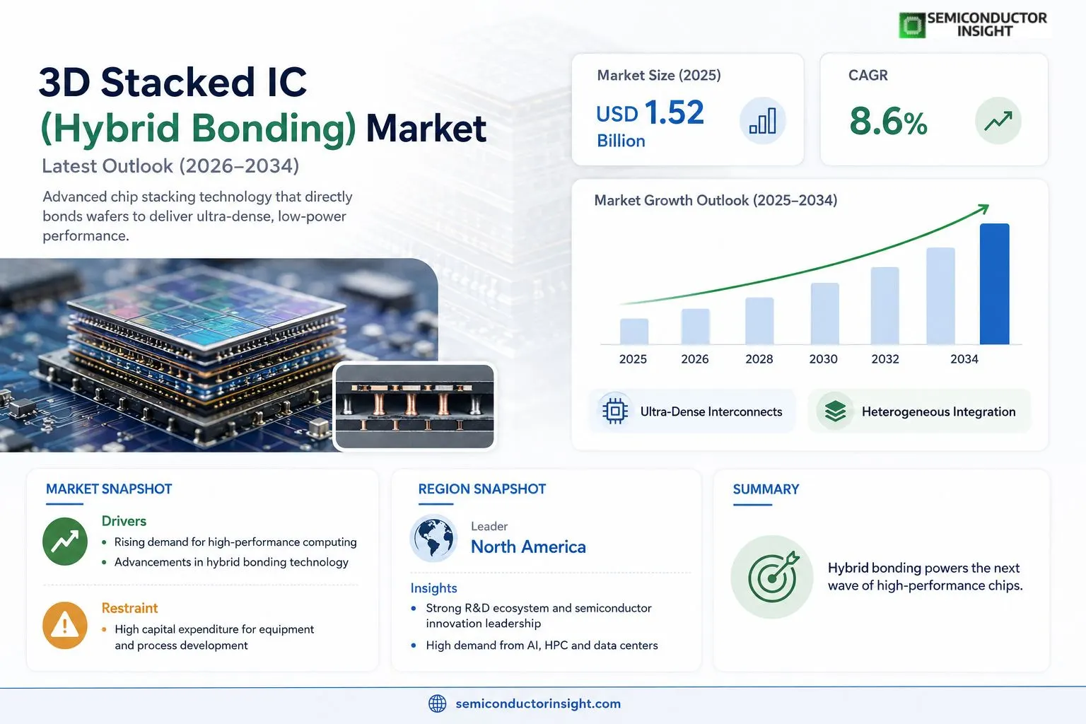
Global 3D Stacked IC (Hybrid Bonding) market size was valued at USD 1.52 billion in 2025. The market is projected to grow from USD 1.58 billion in 2026 to USD 3.24 billion by 2034, exhibiting a CAGR of 8.6% during the forecast period.
Hybrid bonding enables ultra‑dense vertical interconnects by directly bonding wafer surfaces at the nanoscale, combining both metallic and dielectric connections without the need for traditional solder bumps. This technology underpins advanced heterogeneous integration, allowing logic, memory, and sensor dies to be stacked with minimal signal loss and superior thermal performance.
The market is experiencing rapid expansion due to rising demand for high‑performance computing, AI accelerators, and mobile devices that require compact form factors and low power consumption. Furthermore, increased R&D investments by leading semiconductor manufacturers such as TSMC, Intel and Samsung are accelerating adoption of hybrid bonding in next‑generation products. Collaborative initiatives and strategic acquisitions are also expected to drive further market growth.
MARKET DRIVERS
Growing Demand for High‑Performance Computing
3D Stacked IC (Hybrid Bonding) Market is propelled by the escalating need for compute‑intensive workloads in data centers, AI training, and scientific simulations. System‑level integration enabled by hybrid bonding reduces interconnect latency, delivering the performance gains that leading hyperscale operators require.
Advancements in Hybrid Bonding Technology
Recent refinements in low‑temperature direct‑bond interconnects have improved reliability while lowering thermal budgets. These technical improvements make the technology viable for a broader range of semiconductor nodes, encouraging design teams to adopt stack‑up architectures.
➤ Industry analysts note that the convergence of AI workloads and efficient interconnect solutions is reshaping chip‑design strategies worldwide.
Furthermore, the ability to co‑package heterogeneous functions,such as logic, memory, and analog blocks,within a single stack creates differentiated system‑on‑chip solutions, strengthening the commercial appeal of 3D Stacked IC (Hybrid Bonding) Market.
MARKET CHALLENGES
Manufacturing Complexity
Implementing hybrid bonding requires precise alignment and surface preparation, which increases fab line setup times. The steep learning curve can lead to elevated defect rates during early production cycles, challenging manufacturers that must balance yield with throughput.
Other Challenges
Yield Management
Maintaining consistent wafer‑level yields across multiple stacked dies remains a critical hurdle. Variability in bonding pressure and temperature uniformity can cause localized failures that are difficult to diagnose post‑assembly.
MARKET RESTRAINTS
High Capital Expenditure
Adopting hybrid bonding demands substantial investment in new equipment and process development. Smaller fabs or niche players often lack the financial resources to upgrade, limiting broader market participation and slowing overall adoption rates.
MARKET OPPORTUNITIES
Emerging Applications in AI Edge Devices
Edge AI processors benefit from the reduced form factor and power efficiency offered by stacked architectures. As autonomous vehicles, smart cameras, and IoT gateways require higher compute density within constrained footprints, 3D Stacked IC (Hybrid Bonding) Market is positioned to capture significant design wins in these segments.
3D Stacked IC (Hybrid Bonding) Market Trends
Rising Demand for High‑Performance Computing and AI Acceleration
3D Stacked IC (Hybrid Bonding) Market is experiencing accelerated growth as semiconductor designers prioritize chip architectures that deliver higher compute density while minimizing power draw. Hybrid bonding technology provides ultra‑dense vertical interconnects, enabling logic, memory, and sensor dies to be stacked without traditional solder bumps. This results in lower signal loss, improved thermal pathways, and a compact form factor that aligns with the requirements of data‑center processors, AI accelerators, and next‑generation mobile platforms. Manufacturers are therefore integrating hybrid bonding into product roadmaps to meet the performance expectations of emerging workloads.
Other Trends
Strategic R&D Investments and Collaborative Initiatives
Leading foundries such as TSMC, Intel and Samsung have increased research spending on hybrid bonding, aiming to refine process windows and scale yield. In addition, strategic partnerships and acquisitions are consolidating expertise across wafer‑level packaging and materials science. These collaborations accelerate technology transfer, reduce time‑to‑market for heterogeneous integration solutions, and create a competitive ecosystem that supports broader adoption across multiple device categories.
Expansion into Heterogeneous System‑in‑Package (SiP) Applications
Beyond traditional CPU‑memory stacking, 3D Stacked IC (Hybrid Bonding) Market is extending into heterogeneous SiP configurations where analog, RF, and power components coexist with digital logic. This trend is driven by the need for miniaturized modules that combine diverse functions while maintaining signal integrity. As design tools evolve to handle multi‑die thermal and mechanical analysis, vendors are able to offer turnkey solutions that integrate sensors, photonics, and power management ICs within a single stack, further broadening the market’s addressable segments.
COMPETITIVE LANDSCAPEKey Industry Players
3D Stacked IC (Hybrid Bonding) Market Competitive Overview
3D Stacked IC (Hybrid Bonding) Market is dominated by three wafer‑fab powerhouses,TSMC, Intel and Samsung Electronics,each leveraging massive R&D budgets to integrate hybrid‑bonded logic, memory and sensor dies at sub‑micron pitch. These leaders command the bulk of volume shipments, have secured strategic alliances with device manufacturers, and have begun to monetize the technology through high‑performance computing (HPC) and AI accelerator products. The market structure reflects a concentration of capability in advanced 300 mm fabs, where the economics of hybrid bonding demand high wafer throughput and sophisticated process control, creating steep entry barriers for newcomers.Beyond the tier‑one founders, a robust ecosystem of specialized players augments the value chain. ASE Technology Holding and Amkor Technology provide advanced packaging and test services that enable design‑win integration for OEMs. GlobalFoundries, STMicroelectronics and NXP Semiconductors pursue niche applications such as automotive radar and IoT sensors, while Infineon Technologies focuses on power‑aware stacked solutions. Micron Technology contributes memory‑centric hybrid stacks, and IBM explores research‑grade heterogeneous integration. Equipment suppliers like Applied Materials and Lam Research underpin the process with atomic‑layer deposition and wafer‑bonding tools, ensuring that the supply chain can meet the projected 8.6 % CAGR through 2034.
List of Key 3D Stacked IC (Hybrid Bonding) Companies Profiled
- TSMC
- Intel
- Samsung Electronics
- ASE Technology Holding
- Amkor Technology
- GlobalFoundries
- STMicroelectronics
- NXP Semiconductors
- Infineon Technologies
- Micron Technology
- IBM
- Texas Instruments
- Applied Materials
- Lam Research
Segment Analysis:
| Segment Category | Sub-Segments | Key Insights |
| By Type |
|
Hybrid Bonding drives the core value proposition of the market, offering several qualitative advantages:
|
| By Application |
|
High‑Performance Computing emerges as the leading application segment, delivering strategic benefits:
|
| By End User |
|
Semiconductor Manufacturers represent the primary end‑user group, drawing strategic value from hybrid bonding:
|
| By [Segment Category 3]] |
|
N/A |
| By [Segment Category 4]] |
|
N/A |
Regional Analysis: North America
United States
The demand for 3D Stacked IC in AI and HPC is rapidly growing, driven by the need for greater computational power and reduced latency in data centers and cloud computing environments. Hybrid bonding facilitates the integration of multiple chiplets, leading to enhanced performance and energy efficiency for complex workloads.
The 3D stacking technology is increasingly being adopted in advanced mobile devices to achieve higher integration, improved performance, and smaller form factors. This trend is particularly relevant for smartphones, wearables, and other portable electronic devices where space and power consumption are critical considerations.
The automotive industry is embracing 3D Stacked IC for advanced driver-assistance systems (ADAS), autonomous driving capabilities, and infotainment systems. The technology enables higher processing power and improved reliability in challenging automotive environments.
The aerospace and defense sectors are utilizing 3D Stacked IC for critical applications requiring high reliability, performance, and miniaturization. This includes radar systems, electronic warfare systems, and secure communication devices.
Europe
Europe is witnessing a steady growth in 3D Stacked IC (Hybrid Bonding) Market. Several countries, including Germany, the United Kingdom, and France, are investing significantly in semiconductor research and development, fostering innovation in this area. The automotive and industrial sectors are key drivers of demand in the region. Collaboration among European research institutions and industry players is also contributing to the advancement of hybrid bonding technologies. While the adoption rate might be slightly lower compared to North America, Europe presents a promising long-term growth opportunity. The focus here is on sustainable and energy-efficient solutions utilizing 3D stacked IC.
Asia-Pacific
Asia-Pacific is emerging as a significant and rapidly growing market for 3D Stacked IC (Hybrid Bonding). Countries like China, Japan, and South Korea are major players in the global semiconductor industry and are actively investing in 3D integration technologies. The demand is primarily driven by the burgeoning consumer electronics market, the expanding AI and HPC sectors, and the growth of the automotive industry. Government support and large-scale investments in infrastructure are further fueling market expansion. The Asia-Pacific region is expected to become the largest consumer of 3D stacked IC in the coming years. There’s a strong emphasis on cost-effectiveness and high-volume production.
South America
3D Stacked IC (Hybrid Bonding) Market in South America is currently in its nascent stage but holds potential for future growth. The increasing adoption of digital technologies across various industries, including telecommunications, consumer electronics, and industrial automation, is expected to drive demand. However, limited R&D investments and a less mature semiconductor ecosystem are hindering market development. Government initiatives to promote technological advancement and attract foreign investment could catalyze growth in the region. The initial focus will likely be on specific applications with high value-added potential.
Middle East & Africa
The Middle East & Africa region represents a smaller but potentially growing market for 3D Stacked IC (Hybrid Bonding). The increasing investments in infrastructure development, particularly in areas like smart cities and telecommunications, are expected to create demand. The growing adoption of digital technologies and the increasing focus on technological self-sufficiency are also contributing factors. However, the region faces challenges such as limited R&D capabilities and a less developed semiconductor industry. Strategic investments and partnerships could unlock the growth potential of this market segment.
Report Scope
This market research report provides a comprehensive analysis of the 3D Stacked IC (Hybrid Bonding) Market , covering the forecast period 2026–2034. It offers detailed insights into market dynamics, technological advancements, competitive landscape, and key trends shaping the industry.
Key focus areas of the report include:
- Market Overview: The report begins with an overview outlining its current market scenario, key growth indicators, and industry transformation drivers. It discusses macroeconomic factors, demand–supply balance, regulatory landscape, and the strategic role of semiconductors in powering advancements across industries such as automotive, telecommunications, consumer electronics, and industrial automation.
- Market Size & Forecast: Historical data and future projections for revenue, unit shipments, and market value across major regions and segments.
- Segmentation Analysis: Detailed breakdown by product type, technology, application, and end-user industry to identify high-growth segments and investment opportunities.
- Regional Insights: Insights into market performance across North America, Europe, Asia-Pacific, Latin America, and the Middle East & Africa, including country-level analysis where relevant.
- Competitive Landscape: Profiles of leading market participants, including their product offerings, R&D focus, manufacturing capacity, pricing strategies, and recent developments such as mergers, acquisitions, and partnerships.
- Technology Trends & Innovation: Assessment of emerging technologies, integration of AI/IoT, semiconductor design trends, fabrication techniques, and evolving industry standards.
- Market Drivers & Restraints: Evaluation of factors driving market growth along with challenges, supply chain constraints, regulatory issues, and market-entry barriers.
- Stakeholder Insights: Insights for component suppliers, OEMs, system integrators, investors, and policymakers regarding the evolving ecosystem and strategic opportunities.
Primary and secondary research methods are employed, including interviews with industry experts, data from verified sources, and real-time market intelligence to ensure the accuracy and reliability of the insights presented.
FREQUENTLY ASKED QUESTIONS:
What is the current market size of 3D Stacked IC (Hybrid Bonding) Market?
-> 3D Stacked IC (Hybrid Bonding) Market was valued at USD 1.52 billion in 2025 and is expected to reach USD 3.24 billion by 2034.
Which key companies operate in 3D Stacked IC (Hybrid Bonding) Market?
-> Key players include Axalta Coating Systems, AkzoNobel, BASF SE, PPG, Sherwin-Williams, and 3M, among others.
What are the key growth drivers?
-> Key growth drivers include railway infrastructure investments, urbanization, and demand for durable coatings.
Which region dominates the market?
-> Asia-Pacific is the fastest-growing region, while Europe remains a dominant market.
What are the emerging trends?
-> Emerging trends include bio-based coatings, smart coatings, and sustainable rail solutions.

Get Sample Report PDF for Exclusive Insights
Report Sample Includes
- Table of Contents
- List of Tables & Figures
- Charts, Research Methodology, and more...
 Download Sample Report PDF


