Gold Bump Market Insights
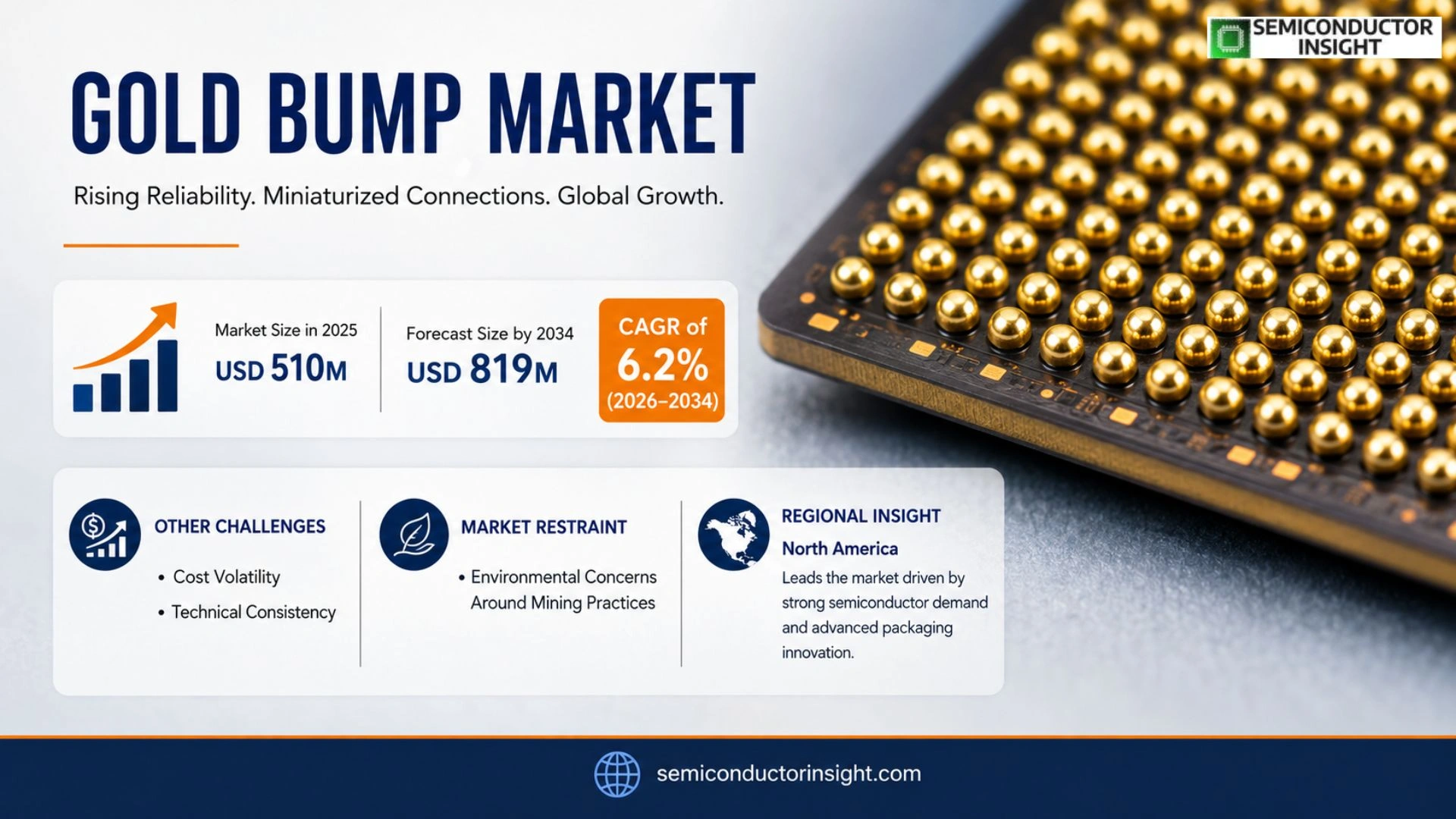
Gold Bump market was valued at USD 510 million in 2025 and is forecasted to attain USD 819 million by 2034, at a CAGR of 6.2 % during the forecast period.
Gold Bump technology involves creating minute gold protrusions on semiconductor dies that serve as interconnect structures in high‑density packaging and display driver IC applications. These bumps are produced through electroplating or stud‑bump bonding, delivering excellent electrical conductivity, oxidation resistance, and mechanical reliability. The technology is divided into plated gold bumps,suitable for high‑throughput wafer‑level processes,and stud gold bumps,preferred for low‑volume, high‑mix production runs.
The sector expands because demand for high‑resolution displays, wearable devices, and compact mobile modules continues to rise. Innovations such as sub‑20 µm pitch designs, thinner bump heights, and integration with hybrid bonding or thermo‑compression bonding push performance limits further. Companies are also exploring AuSn alloy bumping to improve joint reliability and reflow compatibility, while manufacturers report steady price pressure mitigated by higher volume orders from COF, COG, CSP, CMOS image sensor and MEMS producers.
MARKET DRIVERS
Consumer Preference for Premium Finishes
The rising appetite for premium‑grade products has nudged manufacturers toward Gold Bump marke. Shoppers increasingly equate a gold‑toned surface with durability and status, prompting brands to embed gold‑bump technologies into their portfolios. This cultural tilt reshapes purchasing criteria, making the gold finish an implicit value‑add rather than a decorative afterthought.
Innovation in Deposition Techniques
Advances in low‑temperature sputtering and electro‑plating have lowered entry barriers for small and midsize firms. The technical ease of applying a uniform gold bump layer translates into shorter time‑to‑market cycles, allowing companies to respond swiftly to fashion cycles and limited‑edition releases. Consequently, product pipelines are becoming richer and more responsive.
➤ Manufacturers that integrate real‑time monitoring of thickness and adhesion are positioning themselves ahead of peers who rely on legacy batch processes.
Supply‑chain visibility improvements, especially in recycled gold streams, have further buttressed the market. When recyclers guarantee consistent purity, downstream users face fewer compliance headaches, reinforcing confidence across the value chain.
MARKET CHALLENGES
Regulatory Scrutiny Over Precious Metal Content
Authorities across major economies have tightened reporting requirements for precious‑metal content in consumer goods. Compliance incurs additional testing costs and documentation overhead, which especially strains startups that lack dedicated regulatory teams.
Other Challenges
Cost Volatility
Fluctuations in global gold prices create budgeting uncertainty. When spot prices swing sharply, manufacturers must decide whether to lock in forward contracts or absorb higher material costs, a decision that directly impacts margin stability.
Technical Consistency
Maintaining a uniform bump thickness across large batches remains a technical hurdle. Inconsistent application can lead to visual defects that erode brand perception, prompting firms to invest heavily in quality‑control instrumentation.
MARKET RESTRAINTS
Environmental Concerns Around Mining Practices
Public awareness of the ecological footprint associated with primary gold extraction is shaping purchasing behaviour. Brands that cannot demonstrate responsible sourcing face reputational setbacks, limiting their ability to market gold‑bump products at premium price points.
MARKET OPPORTUNITIES
Expansion into Wearable Technology
The convergence of fashion and function in wearables opens a niche for gold‑bump finishes on smart accessories. Designers are seeking materials that combine aesthetic appeal with conductive properties, and gold’s inherent conductivity meets that dual demand. Early adopters that secure design patents stand to capture a loyal segment of tech‑savvy consumers.
Gold Bump Market Trends
Evolution Toward Sub‑20 µm Pitch and Hybrid Bonding
The most visible shift in Gold Bump marke is the drive to shrink bump pitch below 20 µm while simultaneously reducing bump height. This engineering direction is a direct response to the need for denser interconnects in ultra‑high‑resolution display drivers and compact imaging modules. By tightening the pitch, manufacturers can place more I/O points on a single die, which enables higher pixel counts without enlarging the package footprint. The concurrent introduction of hybrid bonding and thermo‑compression bonding techniques creates a pathway for integrating gold bumps with copper‑to‑copper interfaces, delivering lower electrical resistance and improved thermal pathways. Companies that master this combination stand to secure design wins in premium smartphones, augmented‑reality headsets, and automotive heads‑up displays, where both performance and form‑factor constraints are unforgiving.
Other Trends
Material Innovation and Reliability Focus
Beyond geometric scaling, the industry is experimenting with AuSn alloy formulations. The alloy adds tin to the gold matrix, which raises the melting point margin and mitigates re‑flow stress during subsequent assembly steps. This adjustment is particularly valuable for medical and aerospace devices, where long‑term joint stability under temperature cycling is a non‑negotiable requirement. Suppliers that can guarantee consistent alloy composition across wafer‑level batches are beginning to differentiate themselves through higher first‑pass yield rates, translating into lower total cost of ownership for OEMs.
Application‑Driven Diversification
While traditional deployments remain strong in chip‑on‑film and chip‑on‑glass modules, newer segments such as fingerprint sensors, RFID tags, and micro‑electromechanical systems are rapidly adopting gold bump interconnects. The common denominator is the demand for highly uniform, planar bumps that preserve signal integrity at fine pitches. In wearable electronics, for example, the move toward flexible substrates forces designers to select interconnects that can tolerate bending without cracking; gold’s intrinsic ductility and oxidation resistance make it a logical choice. As product cycles shorten, manufacturers that provide a seamless transition from prototype to high‑volume production,leveraging both plated and stud bump processes,will capture a larger share of these emerging niches.
COMPETITIVE LANDSCAPE
Key Industry Players
Gold Bump Market – Competitive Overview
The market is anchored by a handful of firms that control the bulk of wafer‑level production capacity. Nepes, for example, leverages its deep integration with semiconductor fabs in China to offer both plated‑gold and stud‑bond offerings, allowing it to capture high‑mix, low‑volume orders that require tight pitch control. LB Semicon Inc. differentiates itself through a vertically integrated supply chain that reduces cycle time for high‑throughput customers in display driver IC and CMOS image sensor segments. Both companies have broadened their product portfolios to include AuSn alloy variants, reflecting a strategic push toward joint reliability in heterogeneous packaging. Their ability to combine process scale with engineering flexibility creates a barrier for newcomers, while also setting price expectations that shape the overall market structure.
Beyond the dominant trio, a cadre of specialized vendors fills niche roles that sustain the ecosystem. ChipMOS Technologies and Chipbond Technology Corporation have built reputations on rapid prototyping for emerging wearable and biometric modules, often winning contracts that larger players overlook. Steco and Hefei Chipmore Technology focus on sub‑20 µm pitch engineering, catering to ultra‑fine interconnect demands in flagship smartphones. Companies such as Union Semiconductor (Hefei) Co., Ltd., Shenzhen TXD Technology, Jiangsu Yidu Technology, Tongfu Microelectronics (TFME), and China Wafer Level CSP Co., Ltd. concentrate on regional customer bases, providing localized support and cost‑effective solutions for mid‑tier OEMs. Their collective presence ensures that supply remains agile across varied application verticals, from fingerprint sensors to optical modules, and mitigates concentration risk for end users.
List of Key Gold Bump Companies Profiled
- Nepes
- LB Semicon Inc.
- ChipMOS Technologies
- Chipbond Technology Corporation
- Steco
- Hefei Chipmore Technology
- Union Semiconductor (Hefei) Co., Ltd.
- Shenzhen TXD Technology
- Jiangsu Yidu Technology
- Tongfu Microelectronics (TFME)
- China Wafer Level CSP Co., Ltd.
- Advanced Gold Bump Solutions
- GP Semicon
- Micronova Technologies
- EuroGold Packaging
Segment Analysis:
| Segment Category | Sub-Segments | Key Insights |
| By Type |
|
Plated Gold Bumps
|
| By Application |
|
Display Driver IC
|
| By End User |
|
Mobile Devices
|
| By Manufacturing Process |
|
Electroplating
|
| By Device Category |
|
High‑Resolution Displays
|
Regional Analysis: Gold Bump Market
North America
Asset managers are allocating larger slices of discretionary portfolios to gold‑bump instruments, attracted by the perceived low‑correlation to equities and the ability to capture short‑term price spikes. This trend is especially evident among pension funds seeking to diversify risk buffers.
The U.S. Commodity Futures Trading Commission has issued detailed guidance that clarifies reporting obligations for gold‑bump contracts, reducing uncertainty for market participants and encouraging broader participation.
Refiners and custodians are deploying blockchain‑based provenance tools, ensuring that the underlying gold reserves backing bump products are transparent and audit‑ready, which bolsters investor confidence.
High‑net‑worth individuals are increasingly accessing gold‑bump strategies via bespoke advisory platforms, valuing the ability to capture short‑term gold price dynamics while maintaining liquidity.
Europe
European markets exhibit a cautious but growing appetite for Gold Bump marke. Wealth managers in the United Kingdom and Germany are experimenting with structured products that embed gold‑bump exposure, motivated by client demand for assets that can hedge inflation without sacrificing return potential. Regulatory nuance across the EU,particularly the MiFID II framework,forces firms to articulate risk‑adjusted returns with precision, prompting a surge in sophisticated modelling techniques. Moreover, the continent’s strong network of bullion banks facilitates smoother settlement, reducing friction for cross‑border transactions. As the regulatory environment stabilizes, Europe is poised to transition from experimental pilots to more systematic allocation strategies.
Asia‑Pacific
The Asia‑Pacific region is characterized by a blend of rapid wealth creation and a cultural affinity for precious metals, positioning it as a future catalyst for Gold Bump marke. In Hong Kong and Singapore, private banks are packaging gold‑bump strategies within multi‑asset envelopes to satisfy ultra‑high‑net‑worth investors seeking diversification. Meanwhile, emerging economies such as India and China see retail participation rise as fintech platforms introduce simplified interfaces for buying and selling gold‑linked contracts. Although regulatory frameworks differ markedly,China’s tighter capital controls versus Singapore’s open market stance,the overall trajectory points toward deeper market penetration, especially as digital onboarding reduces entry barriers.
South America
South American economies, particularly Brazil and Chile, are beginning to recognize Gold Bump marke as an alternative hedge against volatile commodity cycles. Regional banks are collaborating with international custodians to offer bundled products that combine traditional gold holdings with short‑term price‑bump features. This hybrid approach appeals to corporate treasurers looking to protect cash reserves while retaining upside potential. Despite occasional macro‑economic turbulence, the region benefits from abundant local gold mining activity, which creates a natural supply base and supports the credibility of bump instruments anchored to domestic production.
Middle East & Africa
In the Middle East and Africa, sovereign wealth funds and family offices are the primary architects of Gold Bump Market exposure. Gulf investors leverage the region’s tax‑advantaged environment to allocate capital toward gold‑bump contracts that complement their broader precious‑metal portfolios. In Africa, mining conglomerates are partnering with offshore financiers to securitize future gold output via bump‑linked derivatives, thereby unlocking early‑stage cash flow. Such structures align with the strategic objective of converting physical reserves into liquid financial assets, a shift that could stimulate broader market liquidity if replicated across additional jurisdictions.
Report Scope
This market research report provides a comprehensive analysis of the Gold Bump Market , covering the forecast period 2026–2034. It offers detailed insights into market dynamics, technological advancements, competitive landscape, and key trends shaping the industry.
Key focus areas of the report include:
- Market Overview: The report begins with an overview outlining its current market scenario, key growth indicators, and industry transformation drivers. It discusses macroeconomic factors, demand–supply balance, regulatory landscape, and the strategic role of semiconductors in powering advancements across industries such as automotive, telecommunications, consumer electronics, and industrial automation.
- Market Size & Forecast: Historical data and future projections for revenue, unit shipments, and market value across major regions and segments.
- Segmentation Analysis: Detailed breakdown by product type, technology, application, and end-user industry to identify high-growth segments and investment opportunities.
- Regional Insights: Insights into market performance across North America, Europe, Asia-Pacific, Latin America, and the Middle East & Africa, including country-level analysis where relevant.
- Competitive Landscape: Profiles of leading market participants, including their product offerings, R&D focus, manufacturing capacity, pricing strategies, and recent developments such as mergers, acquisitions, and partnerships.
- Technology Trends & Innovation: Assessment of emerging technologies, integration of AI/IoT, semiconductor design trends, fabrication techniques, and evolving industry standards.
- Market Drivers & Restraints: Evaluation of factors driving market growth along with challenges, supply chain constraints, regulatory issues, and market-entry barriers.
- Stakeholder Insights: Insights for component suppliers, OEMs, system integrators, investors, and policymakers regarding the evolving ecosystem and strategic opportunities.
Primary and secondary research methods are employed, including interviews with industry experts, data from verified sources, and real-time market intelligence to ensure the accuracy and reliability of the insights presented.
FREQUENTLY ASKED QUESTIONS:
What is the current market size of Gold Bump Market?
-> Gold Bump market was valued at USD 510 million in 2025 and is forecasted to attain USD 819 million by 2034, at a CAGR of 6.2 % during the forecast period.
Which key companies operate in Gold Bump Market?
-> Key players include Nepes, LB Semicon Inc, ChipMOS TECHNOLOGIES, Chipbond Technology Corporation, Steco, Hefei Chipmore Technology, Union Semiconductor (Hefei) Co., Ltd., Shenzhen TXD Technology, Jiangsu Yidu Technology, Tongfu Microelectronics (TFME), China Wafer Level CSP Co., Ltd.
What are the key growth drivers?
-> Key growth drivers include the rising demand for high‑resolution displays, wearable electronics, 3D sensing modules, ultra‑compact mobile devices, and the push toward sub‑20 µm pitch and thinner bump heights, which require advanced Gold Bump solutions.
Which region dominates the market?
-> Asia dominates Gold Bump marke, driven by high-volume semiconductor manufacturing in China, Japan, and South Korea, while also showing strong growth potential in other regions.
What are the emerging trends?
-> Emerging trends include sub‑20 µm pitch Gold Bump technology, integration with hybrid bonding and thermo‑compression bonding (TCB), and the development of AuSn alloy bumping to improve joint reliability and reflow compatibility.

Get Sample Report PDF for Exclusive Insights
Report Sample Includes
- Table of Contents
- List of Tables & Figures
- Charts, Research Methodology, and more...
 Download Sample Report PDF