
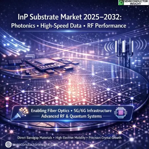
InP Substrate Market: Supporting Next-Gen Photonics and High-Frequency Electronics
InP (Indium Phosphide) Substrate Market refers to the global ecosystem of high-performance substrates made from indium phosphide crystals that serve as the foundational layer for photonic, optoelectronic, and high-frequency electronic devices. In contrast to silicon, InP offers superior electron velocity, direct bandgap properties, and high-frequency performance making it ideal for lasers, photodetector, modulators, and RF amplifiers used in fibre-optic networks, 5G/6G infrastructure, and emerging quantum systems.
InP substrates are not commodity wafers; they are precision engineered materials whose quality directly impacts yield, reliability, and performance of entire semiconductor systems.
Why Demand for InP Substrates Is Growing?
Photonics and High-Speed Data Transfer
One of the most important drivers of InP demand is the surge in data traffic and bandwidth requirements. Global data consumption continues to rise, fueled by streaming, cloud computing, and digital enterprise platforms. Optical communication systems rely on InP-based laser and photonic components for high-speed, low-power, and error-resilient data transfer over fibre.
Where silicon photonics has made strides, InP remains indispensable for wavelengths and performance points silicon devices cannot efficiently reach. This makes InP substrates the material of choice for long-haul optical networks, DWDM systems, and advanced transceivers.
RF and Millimeter-Wave Electronics
Another expanding application domain for InP substrates is high-frequency RF and millimetre-wave electronics. InP devices support blow-off electron speeds and high breakdown voltages critical for 5G base station amplifiers and radar systems. As markets adopt higher frequency bands toward 6G and beyond, the performance envelope of silicon and GaAs is challenged, positioning InP as a strategic material for front-end RF modules.
This type of demand comes less from consumer devices and more from carrier infrastructure, defence platforms, and aerospace systems.
Material Properties Driving Competitive Adoption
Indium phosphide’s appeal lies in its direct bandgap, which allows it to efficiently generate and absorb light an essential property for photonic devices. Its high electron mobility also means faster signal propagation compared to silicon.
However, producing defect-free InP substrates is technically demanding. Uniform crystal growth, precise lattice integrity, and low dislocation density are all necessary to ensure consistent device performance across large wafer areas.
These material characteristics translate into premium pricing and high qualification requirements, but also into distinct performance advantages that justify the investment in advanced applications.
Global Supply Dynamics and Regional Manufacturing Patterns
Asia-Pacific as Manufacturing Hub
Asia-Pacific particularly China, Japan, South Korea, and Taiwan dominates InP substrate production and downstream photonic assembly. Heavy investment in optical communications and 5G infrastructure has made the region the largest adopter and producer of InP-based modules.
China, in particular, has scaled substrate growth capacity and downstream compound semiconductor fabrication in support of domestic networking and defence priorities.
North America and Europe Lead Innovation
While Asia-Pacific leads in volume, North America and Europe remain strong in research-driven markets and niche, high-performance applications. Defence, aerospace, high-end telecom, and research institutions continue to develop advanced InP platforms, investing in innovation far upstream of mass production.
Both regions benefit from strong intellectual property ecosystems, experienced process engineers, and established photonics clusters.
Supply Chain Considerations and Long Qualification Cycles
InP substrates need longer qualifying times than silicon wafers. Engineers must validate not only physical dimensions and crystallographic purity, but also substrate performance under high optical and electrical stresses.
This leads to:
- Longer qualification timelines with device OEMs
- Higher upfront sampling and testing costs
- Less commodity-like purchasing behavior, with emphasis on supplier reliability
Because device performance is tightly coupled with substrate quality, InP substrate suppliers are often long-term partners with their downstream OEMs.
Market Challenges and Material Constraints
Despite compelling performance characteristics, several structural challenges temper market growth:
- Limited Raw Material Availability
Indium is a relatively scarce element, often obtained as a by-product of zinc refinement. Wider adoption of InP substrates increases pressure on indium supply, potentially affecting pricing volatility.
- Manufacturing Complexity
Crystal growth for large-diameter, defect-free InP wafers remains technically challenging and expensive. This restricts capacity expansion and limits production flexibility compared to silicon.
Competition from Alternative Materials
Materials like GaN, Si photonics, and InGaAs/AlGaAs systems compete in overlapping application spaces. While none fully replace InP for certain photonic functions, competition shapes pricing and investment decisions.
Emerging Trends and Future Opportunities
- Integrated Photonics and Co-Packaged Optics
Growth in data centres and AI accelerators is accelerating co-packaged optics and integrated photonics applications where InP functions as a linchpin material for active optical components.
- Microwave and Terahertz Electronics
Higher frequency demand in defence, satellite communication, and automotive radar expands the need for InP RF substrates and heterostructures.
- Quantum and Specialty Research
Quantum computing and advanced sensing research still require bespoke InP platforms due to their material versatility and optical interaction strengths.
At Last before Ending, Don’t Forget to Browse Our Recent Exclusive Report for Detailed Insights:
https://semiconductorinsight.com/report/inp-substrate-market/
Investor Perspective and Market Outlook
From an investment standpoint, the InP substrate market is strategic rather than high-volume. It is not a commodity semiconductor substrate but a critical performance enabler for high-bandwidth and high-frequency applications.
Investors can look at:
- Capacity expansion tied to photonic infrastructure build-outs
- Niche partnerships between substrate manufacturers and foundries
- Upstream raw material hedging strategies
- Service differentiation through substrate traceability and lifecycle support
In the face of evolving network architectures and growing data demand, InP substrates are positioned as enablers of next-generation optical and RF semiconductor solutions.

Comments (0)