
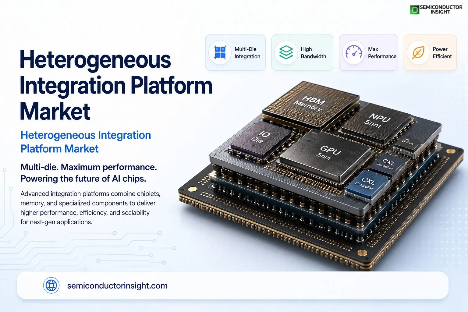
Heterogeneous Integration Platform Market Powers Next Generation AI Chips with Multi-Die Assembly Techniques
Traditional semiconductor manufacturing relied on building entire systems on a single silicon die. That approach hit a wall when physical limits slowed transistor scaling. Gordon Moore himself hinted at an alternative decades ago, suggesting large systems built from smaller, and separately manufactured functions could prove more economical. Today, that vision drives the entire industry forward.
Modern AI accelerators and data centre GPUs cannot fit on one monolithic chip anymore. Computing demands outpaced what a single reticle segment can deliver. The industry responded by combining specialised chiplets, logic, memory, RF, and power components into unified packages. This shift from system-on-chip to system-in-package marks the defining transformation in semiconductor history.
Technology Toolbox Matching Applications to Processes
Heterogeneous integration functions like a Swiss army knife for semiconductor engineers. Different applications demand different tools from the technology portfolio. High-performance computing requires hybrid bonding that joins GPU dies with memory stacks at contact grids measuring just a few micrometres. Medical IoT devices need cost-effective fan-out system integration instead.
Level 0 represents the chip itself.
Level 1 integrates chips on a wafer or stacks them vertically.
Level 2 uses organic or glass interposers for connections.
Level 3 employs substrates as system carriers with added functionality.
Fraunhofer IZM’s research demonstrates that this four-level architecture enables miniaturised systems using diverse approaches rather than one-size-fits-all solutions.
Practical Applications Sparking Large-Scale Expansion Momentum
- TSMC secured four major clients for CoWoS packaging AMD, Nvidia, Broadcom, and Apple. The company’s monthly CoWoS capacity reached 35,000 to 40,000 wafers in 2024 and targets 75,000 wafers monthly in 2025, nearly doubling output. By end of 2026, capacity will hit 90,000 wafers per month with the AP8 plant from Innolux coming online.
- Apple commenced M4 chip development using SoIC with hybrid moulding technology. Small-scale trial production began in 2024, with mass production scheduled for 2025. The M4 will likely debut in next-generation MacBook Pro models, potentially using 2nm process nodes.
- Samsung announced mass production of HBM3E with 12-layer stacked DRAM dies in June 2024. AMD’s MI300 integrates more than two large compute dies fabricated on TSMC’s 4nm process alongside multiple HBM stacks.
Open Standards Enabling Cross-Vendor Interoperability
Universal Chiplet Interconnect Express became the industry’s open specification for die-to-die interconnect between chiplets. AMD, Arm, ASE Group, Google Cloud, Intel, Meta, Microsoft, Qualcomm, Samsung, and TSMC co-developed the standard. Alibaba Group and Nvidia joined as board members in August 2022.
- UCIe 3.0, released on August 5, 2025, delivers 48 GT/s and 64 GT/s data rates with runtime recalibration enhancements.
- The extended sideband channel reaches 100mm while supporting continuous transmission protocols.
- Full backward compatibility ensures seamless integration with previous specifications.
Intel’s Foveros technology enables vertical die stacking through hybrid copper bonding with interconnect densities exceeding 10,000 connections. This builds on EMIB by allowing 3D stacking that reduces wire lengths and parasitics while saving massive on-chip real estate.
Performance Gains through Minimised Signal Latency
The core advantage of heterogeneous integration lies in keeping paths between functional units extremely short. Signal latencies drop dramatically when optical, mechanical, and CMOS components combine from their optimised production processes. High-frequency switches no longer share CMOS platforms, requiring different cooling and power delivery.
Shorter signal paths enable 20× better I/O performance and power consumption at approximately 0.5 pJ per bit compared to typical PCIe SerDes. Bandwidth density reaches 1.35 TB/s per mm² for 45 μm bump pitch, climbing 3.24× higher with 25 μm pitch. Edge AI and datacenters benefit critically as memory placement near compute reduces latency for inference and training.
To Know More about the Report, You Can Freely Browse Our Latest Updated Report: https://semiconductorinsight.com/report/heterogeneous-integration-hi-platform-market/
Economic Benefits beyond Pure Performance
Smaller dies improve manufacturing yields significantly. A monolithic 100mm² die failing at 5% has vastly different economics than four 25mm² chiplets each failing at 5%. Reusing proven IP blocks across multiple products cuts development time and cost. Different chiplets from different process nodes and vendors mix within the same package.
Panel-level packaging emerges as a cost-effective alternative to wafer-based methods. Recyclable materials and low-energy processes address sustainability concerns. The ecological footprint quantification becomes essential as resource and energy consumption optimisation drives Green ICT research initiatives.
Applications Spanning Multiple Industries
- High-performance computing, medical technology, mobility, renewable energies, and smart farming all leverage heterogeneous integration differently. Automotive systems for autonomous driving require different components than IoT sensors. Training large language models demands distinct architectures compared to RF communication interfaces.
- Hardware security benefits through distributed manufacturing, avoiding single points of failure. Embedded micro RFID tags in chip rewiring ensure trustworthy supply chains. Anti-tampering features are incorporated into separate functions while maintaining system integrity.
The semiconductor industry transitioned from technology-driven development to application-driven innovation. Artificial intelligence created the hype that brought 3D stacking technologies from filing cabinets into production lines. Market demand now drives technological development rather than the reverse.

Comments (0)