Market Insights
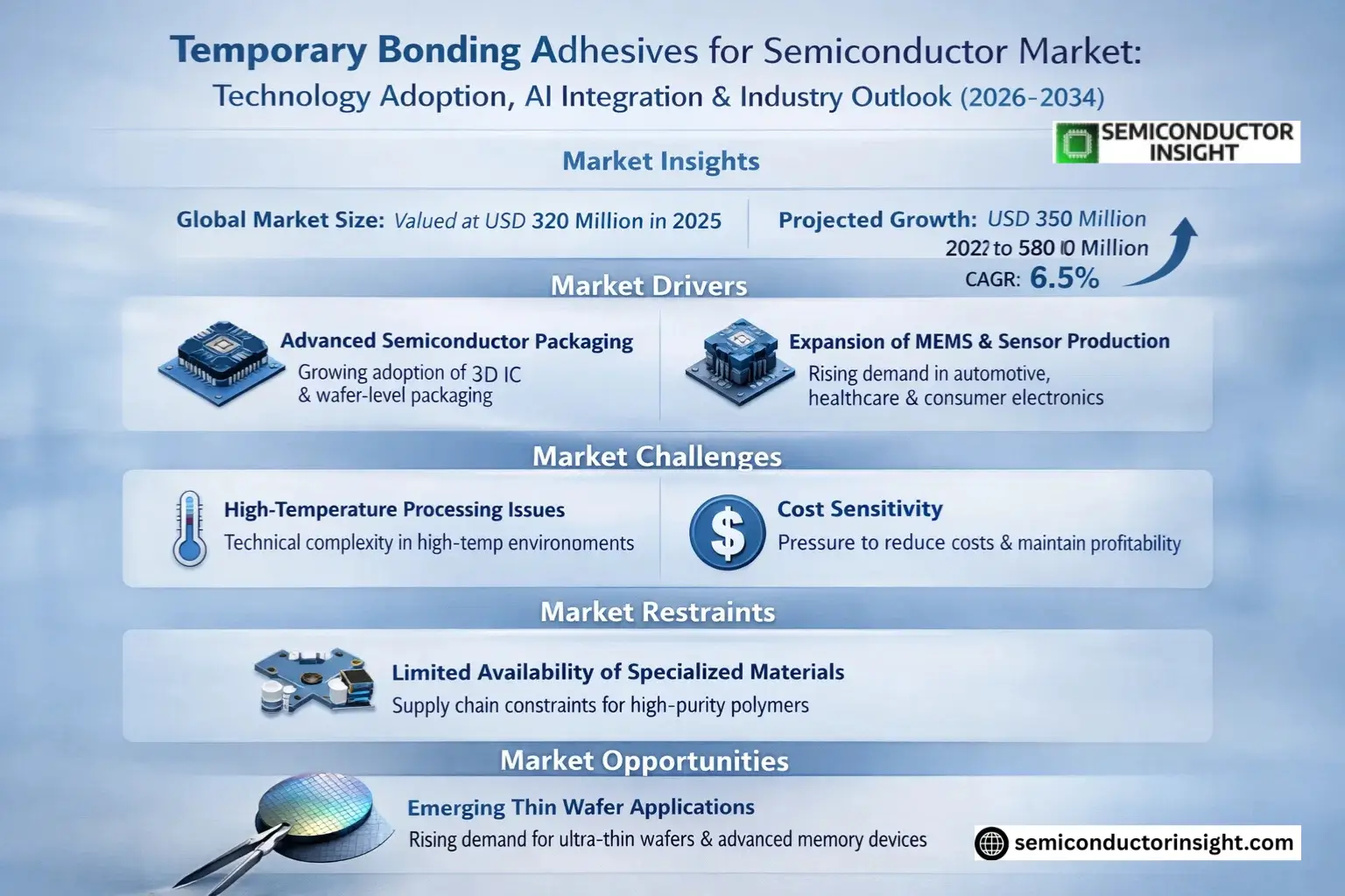
Global Temporary Bonding Adhesives for Semiconductor Market size was valued at USD 320 million in 2025. The market is projected to grow from USD 350 million in 2026 to USD 580 million by 2034, exhibiting a CAGR of 6.5% during the forecast period.
Temporary bonding adhesives for semiconductor applications are specialized materials designed to temporarily secure wafers or chips to carrier substrates during manufacturing processes. These adhesives enable precise handling and protection of delicate semiconductor components through critical fabrication steps such as wafer thinning, backgrinding, and lithography. The technology includes UV-curable and water-soluble formulations that can be cleanly removed after processing without damaging the semiconductor device.
The market growth is driven by increasing demand for advanced packaging solutions in consumer electronics and automotive applications, where thinner and more complex semiconductor devices are required. While wafer-level packaging adoption accelerates growth, challenges remain in developing adhesives that maintain stability under extreme processing conditions. Key players like Brewer Science and Tokyo Ohka Kogyo continue to innovate with low-temperature debonding solutions to address emerging 3D IC packaging requirements.
MARKET DRIVERS
Rising Demand for Advanced Semiconductor Packaging
Temporary Bonding Adhesives for Semiconductor Market is driven by increasing adoption of advanced packaging technologies like 3D IC and wafer-level packaging. These adhesives enable precise handling of ultra-thin wafers during backgrinding and other processes. With semiconductor manufacturers pushing for higher performance in smaller form factors, the need for reliable temporary bonding solutions has grown significantly.
Expansion of MEMS and Sensor Production
Growth in MEMS and sensor applications across automotive, healthcare, and consumer electronics has created substantial demand for temporary bonding adhesives. These specialized adhesives facilitate the manufacturing of delicate microstructures without damage during processing. The market sees particular strength in regions with concentrated semiconductor fabrication facilities.
Increased R&D investments by major adhesive manufacturers to develop low-temperature debonding solutions are further propelling market growth, addressing challenges in advanced node semiconductor fabrication.
MARKET CHALLENGES
Technical Complexity in High-Temperature Processes
Temporary Bonding Adhesives for Semiconductor Market faces challenges in maintaining stability during high-temperature processing while allowing clean debonding. Performance requirements become more stringent with shrinking semiconductor feature sizes, placing significant technical demands on adhesive formulations.
Other Challenges
Process Compatibility Issues
Achieving compatibility with diverse semiconductor materials and subsequent process steps requires continuous adhesive formulation modifications, increasing development costs.
Cost Sensitivity
The semiconductor industry’s focus on cost reduction pressures adhesive manufacturers to deliver high-performance solutions at competitive price points, challenging profit margins.
MARKET RESTRAINTS
Limited Availability of Specialized Materials
Temporary Bonding Adhesives for Semiconductor Market faces constraints due to the limited suppliers of high-purity polymer materials required for these specialized formulations. Supply chain disruptions can significantly impact production capabilities, particularly for critical semiconductor manufacturing processes that cannot tolerate material inconsistencies.
MARKET OPPORTUNITIES
Emerging Thin Wafer Applications
Temporary Bonding Adhesives for Semiconductor Market has significant growth potential in applications requiring ultra-thin wafers below 50μm thickness. As demand increases for power devices and advanced memory solutions, manufacturers are investing in specialized bonding technologies capable of handling these delicate substrates through the entire fabrication process.
Temporary Bonding Adhesives for Semiconductor Market Trends
Rising Demand for Advanced Semiconductor Packaging Solutions
Temporary Bonding Adhesives for Semiconductor Market is experiencing significant growth due to increasing demand for advanced semiconductor packaging. These specialized adhesives enable precise handling during wafer thinning, backgrinding, and other critical semiconductor manufacturing processes. UV-curable type adhesives are gaining prominence as they offer superior processing efficiency compared to traditional alternatives.
Other Trends
Shift Toward Wafer-Level Packaging
The semiconductor industry’s transition to wafer-level packaging is driving adoption of high-performance temporary bonding solutions. Manufacturers require adhesives that maintain stability during thermal cycling while allowing clean debonding. This trend is particularly strong in Asia-Pacific markets where semiconductor production is concentrated.
Regional Market Developments
China and the United States continue to lead in temporary bonding adhesive adoption, with Japan and South Korea showing strong growth in advanced semiconductor applications. European manufacturers are focusing on developing eco-friendly, water-soluble formulations to meet stricter environmental regulations while maintaining performance requirements.
Competitive Landscape Shifts
The market remains competitive with key players like 3M, DELO, and Tokyo Ohka Kogyo investing in research for next-generation formulations. Recent developments include adhesives with improved thermal stability for 3D IC packaging applications and products designed for emerging semiconductor materials such as silicon carbide and gallium nitride.
Technology Advancements Driving Innovation
New adhesive formulations are emerging to address challenges in advanced nodes below 7nm, where process temperatures and mechanical stresses create demanding performance requirements. The industry is seeing increased adoption of temporary bonding solutions that combine high thermal resistance with low-temperature debonding capabilities.
COMPETITIVE LANDSCAPE
Key Industry Players
Global Leaders Drive Innovation in Semiconductor Bonding Adhesives
3M and Brewer Science dominate Temporary Bonding Adhesives for Semiconductor Market, jointly holding approximately 35% of the global revenue share. These industry leaders benefit from extensive R&D capabilities and patented technologies for advanced semiconductor packaging. The market demonstrates moderate consolidation, with the top five players accounting for nearly 60% of 2025 revenues. 3M’s Light Tape products and Brewer Science’s WaferBOND solutions set industry standards for thermal stability and clean debonding in 3D IC applications.
Japanese specialist Tokyo Ohka Kogyo (TOK) leads in high-temperature resistant formulations, while Germany’s DELO dominates precision UV-curable adhesives for thin wafer handling. Niche players like AI Technology and Dynatex International are gaining traction with specialized solutions for MEMS and optoelectronics applications. Emerging innovators such as YINCAE Advanced Materials are developing sustainable, low-outgassing formulations to meet next-generation semiconductor requirements.
List of Key Temporary Bonding Adhesives Companies Profiled
- 3M Company
- Brewer Science
- DELO Industrial Adhesives
- Tokyo Ohka Kogyo Co., Ltd. (TOK)
- AI Technology, Inc (AIT)
- Dynatex International
- Water Wash Technologies LLC
- Daetec LLC
- HD MicroSystems
- Valtech Corporation
- YINCAE Advanced Materials
- Micro Materials Limited
- Shin-Etsu Chemical Co., Ltd.
- Henkel AG & Co. KGaA
- Dow Chemical Company
Segment Analysis:
| Segment Category | Sub-Segments | Key Insights |
| By Type |
|
UV-curable Type dominates the market due to:
|
| By Application |
|
Wafer Thinning and Backgrinding leads application demand because:
|
| By End User |
|
Foundries represent the largest end-user segment due to:
|
| By Technology Readiness |
|
Leading-edge Nodes show strongest growth potential as:
|
| By Product Form |
|
Liquid Adhesives maintain market leadership owing to:
|
Regional Analysis: Asia-Pacific Temporary Bonding Adhesives for Semiconductor Market
Asia-Pacific leads in adopting UV-curable temporary bonding adhesives for 3D IC packaging applications. Manufacturers are rapidly transitioning from traditional thermal release adhesives to photo-degradable formulations that enable precision debonding processes. Taiwan’s semiconductor ecosystem shows particularly strong uptake of these advanced materials.
South Korean semiconductor firms are pioneering AI-driven adhesive application systems that optimize bonding thickness and curing parameters. These smart manufacturing solutions significantly reduce defect rates in wafer thinning processes while improving throughput in advanced packaging lines.
Japan maintains a robust domestic supply of high-performance temporary bonding adhesives through strategic partnerships between material suppliers and semiconductor OEMs. This localized ecosystem ensures reliable access to specialized formulations for memory and logic device production.
The region is expected to maintain leadership through 2034, with China emerging as a major consumer of temporary bonding solutions. Increasing investments in compound semiconductor manufacturing will drive demand for adhesive materials compatible with GaN and SiC wafers.
North America
North America represents a high-value market for temporary bonding adhesives, characterized by extensive R&D activities in advanced packaging technologies. Leading semiconductor equipment manufacturers in Silicon Valley collaborate with material science companies to develop next-generation debonding solutions. The region sees growing adoption of temporary adhesives for heterogeneous integration in AI accelerator chips and high-performance computing applications.
Europe
Europe’s temporary bonding adhesives market benefits from robust automotive semiconductor demand. German and French material suppliers are focusing on developing thermal-stable formulations for power electronics packaging. The region shows increasing interest in environmentally friendly adhesive solutions that comply with strict EU chemical regulations.
South America
South America’s emerging semiconductor test and assembly facilities are creating new opportunities for temporary bonding adhesive suppliers. While the market remains small compared to other regions, Brazil’s growing electronics manufacturing sector shows potential for mid-term growth in adhesive consumption for consumer device packaging.
Middle East & Africa
The MEA region presents niche opportunities in temporary bonding adhesives, primarily serving semiconductor packaging service providers in Israel and South Africa. Market growth is limited by the absence of major semiconductor fabs, though increasing investments in electronics manufacturing infrastructure could change this dynamic.
Report Scope
This market research report provides a comprehensive analysis of the Temporary Bonding Adhesives for Semiconductor Market, covering the forecast period 2025–2034. It offers detailed insights into market dynamics, technological advancements, competitive landscape, and key trends shaping the industry.
Key focus areas of the report include:
- Market Overview: The report begins with an overview outlining its current market scenario, key growth indicators, and industry transformation drivers. It discusses macroeconomic factors, demand–supply balance, regulatory landscape, and the strategic role of temporary bonding adhesives in semiconductor manufacturing processes.
- Market Size & Forecast: Historical data and future projections for revenue, unit shipments, and market value across major regions and segments.
- Segmentation Analysis: Detailed breakdown by product type, technology, application, and end-user industry to identify high-growth segments and investment opportunities.
- Regional Insights: Insights into market performance across North America, Europe, Asia-Pacific, Latin America, and the Middle East & Africa, including country-level analysis where relevant.
- Competitive Landscape: Profiles of leading market participants, including their product offerings, R&D focus, manufacturing capacity, pricing strategies, and recent developments such as mergers, acquisitions, and partnerships.
- Technology Trends & Innovation: Assessment of emerging technologies, including UV-curable and water-soluble adhesive solutions, and their applications in semiconductor manufacturing.
- Market Drivers & Restraints: Evaluation of factors driving market growth along with challenges, supply chain constraints, regulatory issues, and market-entry barriers.
- Stakeholder Insights: Insights for component suppliers, OEMs, system integrators, investors, and policymakers regarding the evolving ecosystem and strategic opportunities.
Primary and secondary research methods are employed, including interviews with industry experts, data from verified sources, and real-time market intelligence to ensure the accuracy and reliability of the insights presented.
FREQUENTLY ASKED QUESTIONS:
What is the current market size of Temporary Bonding Adhesives for Semiconductor Market?
-> Temporary Bonding Adhesives for Semiconductor Market size was valued at USD 320 million in 2025. The market is projected to grow from USD 350 million in 2026 to USD 580 million by 2034, exhibiting a CAGR of 6.5% during the forecast period.
What is the growth rate of Temporary Bonding Adhesives for Semiconductor Market?
-> The market is expected to grow at a CAGR of % during the forecast period 2025-2034.
Which are the key companies in Temporary Bonding Adhesives for Semiconductor Market?
-> Key players include 3M, DELO, Tokyo Ohka Kogyo, AI Technology, Inc (AIT), Dynatex International, Water Wash Technologies, Brewer Science, Daetec, HD MicroSystems, and Valtech Corporation, among others.
Which product type segment shows strong growth potential?
-> The UV-curable Type segment is expected to reach USD million by 2034, with significant growth potential.
What are the major applications of temporary bonding adhesives in semiconductors?
-> Major applications include Wafer Thinning and Backgrinding, Wafer Bonding, Lithography and Patterning, and other semiconductor manufacturing processes.
Get Sample Report PDF for Exclusive Insights
Report Sample Includes
- Table of Contents
- List of Tables & Figures
- Charts, Research Methodology, and more...
 Download Sample Report PDF