
Key Statistics
Key Takeaways
- UV-type wafer tapes hold 62.5% of the current product mix because UV irradiation allows strong wafer holding during grinding or dicing and then sharply reduces adhesion for clean chip pickup.
- Wafer cutting / dicing is the largest application at 54.95% share, while grinding-related demand is rising as advanced packages use thinner wafers, backside processing and more complex bump structures.
- Taiwan is the largest consumption market with 34% share, followed by mainland China at 27.4% and North America at 9.27%. Japan dominates production with 83% output share through a deep specialty-adhesive and semiconductor-materials ecosystem.
- The top five manufacturers hold 82.5% of global supply, led by Mitsui Chemicals, LINTEC, Nitto Denko, Denka and other established Japanese materials companies.
- Advanced packaging is increasing tape value per wafer. LINTEC is investing in new process R&D for HBM, chiplets and direct-bonding workflows, while Nitto offers solvent-resistant dicing tapes for TSV and ultra-thin wafer processing.
Tapes for Semiconductor Manufacturing Process Market Overview
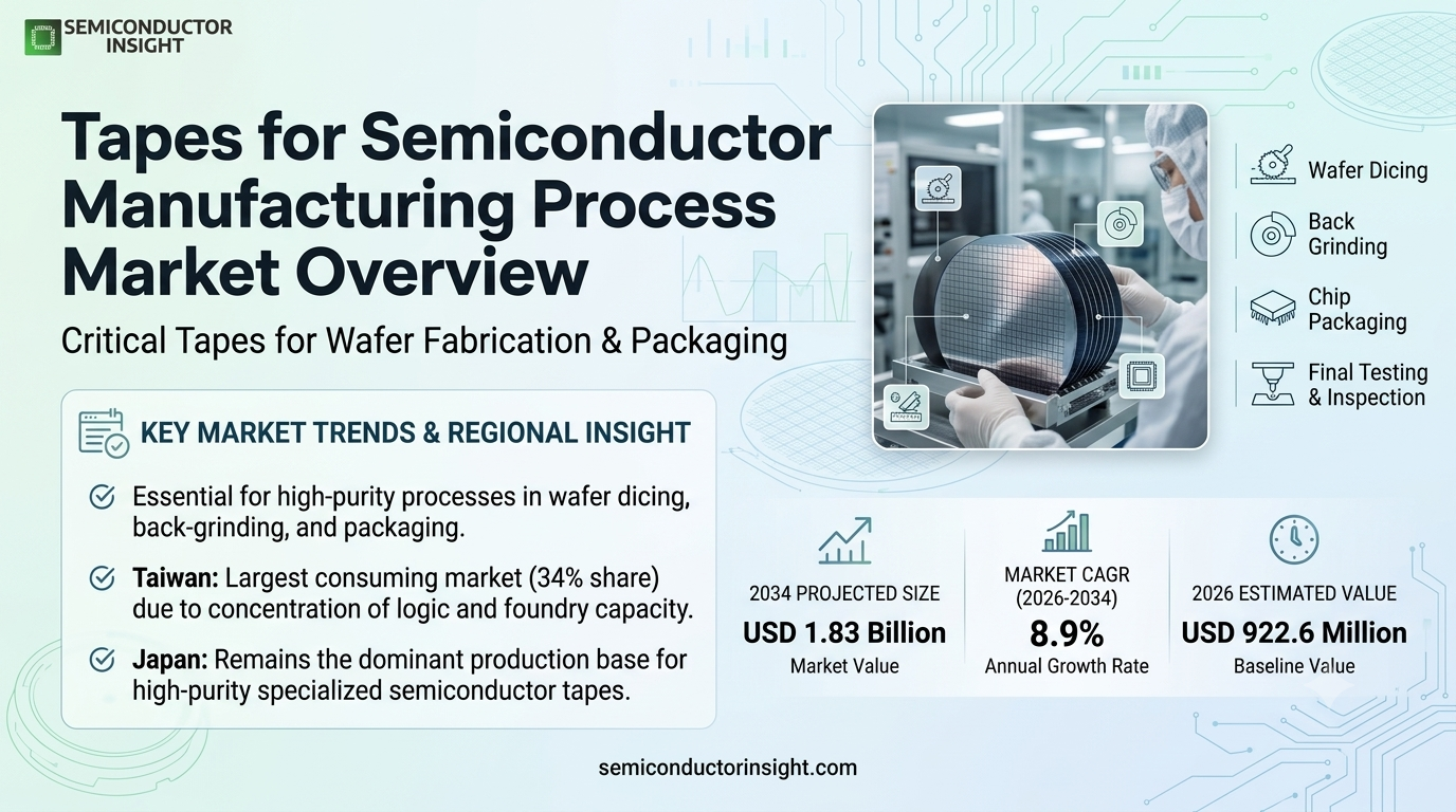
Tapes for Semiconductor Manufacturing Process market was valued at USD 847.0 million in 2025 and is projected to reach USD 1.83 billion by 2034, representing an 8.9% CAGR during 2026–2034. The 2026 estimated market size is USD 922.6 million. Taiwan is the largest consumption market with 34% share, while Japan remains the dominant production base for high-purity semiconductor tapes.
Semiconductor process tapes are engineered adhesive materials used to protect, support, mount or temporarily bond wafers and dies during grinding, dicing, thinning, transfer, molding and packaging. They combine a polymer carrier film with pressure-sensitive adhesive or functional layers designed for controlled adhesion, clean release and low contamination. UV-curable products can hold a wafer securely during processing and then reduce adhesion after irradiation, improving die pickup.
The product specification becomes more demanding as wafers become thinner and package structures more complex. Back grinding can expose wafers to cracking and local thickness variation, while TSV and advanced packaging processes may require solvent resistance, heat tolerance, low outgassing and extremely low ionic contamination. A tape that leaves residue or distorts a thin wafer can create yield loss far greater than the tape’s purchase price.
Materials and equipment are increasingly developed together. LINTEC sells both Adwill tapes and specialized tape application or removal systems, while Nitto combines process tapes with NEL SYSTEM wafer-handling equipment. This integrated approach helps suppliers optimize pressure, lamination, UV exposure and peeling as one process rather than treating the adhesive tape as an isolated consumable.
Segment Analysis: By Type
By type, the market is segmented into UV Type Tapes and Non-UV Type Tapes. UV-type products hold 62.5% share because they provide high holding force during wafer processing and lower adhesion after UV irradiation, which improves clean release and die pickup in dicing and advanced packaging.
| Type | Adhesive behavior | Market position |
|---|---|---|
| UV Type Tapes | UV-curable adhesive maintains strong tack during grinding, dicing or handling and then changes chemistry when exposed to ultraviolet light so the wafer or die can be released with lower peel force. The controlled switch in adhesion reduces pickup damage and residue risk. | Largest type with 62.5% share. UV products are widely used in advanced dicing and wafer-processing flows where strong hold and low-damage release are both required. |
| Non-UV Type Tapes | Non-UV tapes use pressure-sensitive, thermal-release or other adhesive systems that do not require an ultraviolet irradiation step. They can simplify equipment requirements and are suitable where process temperature, chemical exposure or substrate sensitivity favors another release mechanism. | A mature and application-specific segment. Heat-resistant, solvent-resistant and low-adhesion products remain important for specialized wafer and package processing. |
Application and adhesive-technology segmentation
Wafer cutting is the largest application because every singulated die must remain stable during mechanical, laser or plasma dicing. Back grinding is another large segment and becomes more demanding as wafers are thinned for HBM, power devices, WLCSP and stacked packages. Acrylic adhesives lead broadly because they can be tuned across adhesion, UV response, aging and contamination requirements.
| Axis | Segments | Commercial implication |
|---|---|---|
| By Application | Back Grinding · Wafer Cutting / Dicing · Die Bonding / DAF · Surface Protection · Temporary Support · Others | Wafer cutting accounts for 54.95% of current demand. Grinding-related use grows with ultra-thin wafers and backside processing, while integrated dicing-die-attach materials add more functionality per tape layer. |
| By Adhesive Technology | Acrylic · Silicone · Rubber-Based · Functional UV / Thermal Release | Acrylic chemistry offers a broad balance of adhesion and clean release. Silicone supports temperature and specialty surfaces, while UV and thermal-release functions enable tightly controlled process transitions. |
Segment Analysis: By Application
By application, wafer cutting and dicing lead with 54.95% share, followed by back grinding, die bonding, surface protection and other process steps. Advanced packaging increases tape demand because thin wafers and dies move through more temporary-support, debonding and transfer operations before final assembly.
| Application | Key market insight |
|---|---|
| Wafer Cutting / Dicing | Dicing tape holds the wafer and individual chips in position while a blade, laser or plasma process separates die. After cutting, controlled reduction in adhesion allows reliable pickup. UV dicing tapes dominate many advanced processes because they combine strong hold with clean post-irradiation release. |
| Back Grinding | Back grinding tape protects the circuit surface and supports the wafer while the backside is thinned. Bumped wafers can create thickness non-uniformity when conventional tape bridges topography, leading suppliers to develop resins, cushioning structures and process equipment that improve flatness. |
| Die Attach / DAF | Dicing die-bonding film integrates wafer support with the adhesive layer used to attach the die to a substrate or interposer. This can remove a separate dispensing step and improve bond-line control in stacked CSP and advanced packaging. |
| Temporary Support / TSV | Ultra-thin wafers and TSV processes may require solvent-resistant dicing tape or temporary carrier support through cleaning and backside operations. Chemical resistance and easy release are critical because the wafer is mechanically fragile. |
| Surface / Mold Protection | Protective tapes shield sensitive surfaces during molding, grinding, plating or transport. Low residue, heat resistance and particle control are important where contamination can affect bonding or optical performance. |
Regional Analysis
Asia Pacific dominates semiconductor-process tape demand and production. Taiwan is the largest consumer with 34% share, mainland China follows with 27.4%, and North America represents 9.27%. Japan produces 83% of global supply, reflecting the strong positions of Mitsui Chemicals, LINTEC, Nitto Denko, Denka, Furukawa Electric, Sekisui Chemical and other specialty-materials companies.
Why is the market so concentrated in East Asia?
Semiconductor tapes are closely qualified with wafer-processing equipment and fab recipes, so suppliers benefit from proximity to high-volume foundry, memory and packaging clusters. Japan provides the materials and adhesive-technology base, while Taiwan, China and South Korea create large recurring consumption through wafer fabrication and backend manufacturing. Southeast Asia is gaining importance as assembly and packaging capacity diversifies.
| Region | Market position | Growth outlook | Core demand | Commercial priority |
|---|---|---|---|---|
| Japan | 83% production share | High | Materials & tape manufacturing | High-purity chemistry, R&D and customer qualification |
| Taiwan | 34% consumption share | Very high | Foundry & advanced packaging | Local technical support and clean release |
| Mainland China | 27.4% consumption share | Very high | Fab localization & packaging | Local supply, cost and qualification |
| North America | 9.27% consumption share | High | New fabs & advanced packaging | Local support and supply security |
| Other regions | Growing | Moderate | Assembly, automotive & specialty | Availability and process support |
Competitive Landscape
Key participants include Mitsui Chemicals, LINTEC Corporation, Denka, Nitto Denko, Furukawa Electric, Sekisui Chemical, Maxell Sliontec, Resonac, Sumitomo Bakelite, D&X, KGK Chemical, AI Technology, Ultron System, Shanghai Guke Adhesive Tape Technology and Yantai Darbond Technology. The top five manufacturers hold 82.5% of global supply, making qualification history and proprietary adhesive chemistry major competitive barriers.
Mitsui Chemicals’ ICROS tape has been used as a back-grinding tape for decades and now supports multiple semiconductor manufacturing steps. The product family emphasizes ultra-low contamination, tight total-thickness control, easy peel, heat and chemical resistance, and bump absorption. This breadth supports customers as wafer topography becomes more complex.
LINTEC differentiates through integrated materials and equipment. Its Adwill portfolio includes back-grinding, dicing, backside-coating and dicing-die-bonding tapes, while dedicated equipment applies, removes and irradiates tapes. In 2026 the company expanded process-development infrastructure for advanced packaging and announced a major new Semiconductor Solutions Lab.
Nitto provides back-grinding, dicing, die-attach and thermal-release materials plus NEL SYSTEM handling equipment. Its solvent-resistant dicing tape targets TSV and ultra-thin wafer flows where solvent cleaning occurs after temporary carrier removal. Chinese suppliers are gaining share through local supply but must clear strict contamination and reliability validation.
Competitive tier structure
| Competitive tier | Representative companies | Competitive strengths |
|---|---|---|
| Japanese global leaders | Mitsui Chemicals; LINTEC; Nitto Denko; Denka; Furukawa Electric | High-purity adhesive chemistry, global fab qualifications, advanced packaging R&D and process equipment |
| Established specialty suppliers | Sekisui Chemical; Maxell Sliontec; Resonac; Sumitomo Bakelite; KGK Chemical | Functional films, process-specific tapes, thermal / chemical resistance and long semiconductor histories |
| Regional / emerging suppliers | D&X; AI Technology; Ultron System; Shanghai Guke; Yantai Darbond | Local customer support, competitive cost and growing qualification in Asian semiconductor clusters |
Key companies profiled
Semiconductor Process Tape Production & Qualification Analysis
Production capacity combines high-purity polymer synthesis, film formation, precision adhesive coating, cleanroom slitting and final inspection. Semiconductor tape lines must control particles, ionic contamination, thickness and adhesive uniformity far more tightly than ordinary industrial tape. Effective capacity also depends on customer qualification because a roll produced on a new line may not be accepted until process-equivalence testing is complete.
Adhesive formulation and coating quality are critical. Small thickness variation can change wafer flatness during back grinding, while local adhesion variation can cause die shift during dicing. UV-curable products add photochemical performance requirements so adhesion falls predictably after the specified irradiation dose.
Application equipment creates another productivity layer. Tape laminators, peelers and UV systems determine pressure, temperature and release consistency on the customer line. Suppliers that control both tape and equipment can optimize the complete process and shorten troubleshooting time.
Market Dynamics
Growth is driven by semiconductor output, wafer thinning, HBM and advanced packaging, higher cleanliness requirements and new regional fabs. Restraints include long qualification cycles, raw-material purity, contamination risk and supplier concentration. Opportunities center on ultra-thin wafers, direct bonding, solvent-resistant tapes, integrated die-attach films and low-residue sustainable materials.
MARKET DRIVERS
Advanced packaging adds more tape-enabled steps
HBM and chiplet flows thin wafers, cut dies, bond stacks and protect surfaces repeatedly. This increases the number and technical value of tapes used per completed package.
Thinner wafers need better mechanical support
As wafer thickness falls, warpage and cracking risk increase. Back-grinding and support tapes must absorb topography, hold the wafer uniformly and release without damaging thin silicon.
New fabs expand recurring consumables demand
Once a semiconductor line enters qualification and production, tapes are consumed continuously. Regional fab investment therefore translates into recurring materials demand rather than one-time equipment sales.
Cleanliness becomes more valuable at advanced nodes
Particles, ionic contamination and adhesive residue can affect bonding and device reliability. Suppliers with proven low-contamination chemistry can capture premium applications.
Drivers Impact Analysis
| Driver | Impact | Primary markets | Time horizon |
|---|---|---|---|
| Advanced packaging / HBM | High | Taiwan, Korea, Japan, U.S. | Short to long term |
| Wafer thinning and backside processing | High | Global advanced fabs | Persistent |
| Fab capacity expansion | High | Asia, U.S., Europe | Medium to long term |
| Higher cleanliness / residue control | High | Leading-edge processes | Persistent |
MARKET RESTRAINTS
Qualification slows new supplier entry
Tape interacts directly with wafer surfaces and process equipment. Customers validate adhesion, residue, particles, UV response and peel behavior before approving a product, creating long sales cycles.
A small residue can create large yield loss
Adhesive contamination can interfere with bonding, lithography or electrical contact. This makes low-residue performance essential and increases analytical and cleanroom manufacturing cost.
Specialty materials are not commodity inputs
High-purity acrylics, silicones, release films and UV-sensitive components require controlled supply chains. Raw-material changes may trigger customer requalification.
Concentration creates supply risk
A large share of production is concentrated among Japanese suppliers. Geographic disruptions can affect global fabs, encouraging regional inventory and second-source qualification.
Restraints Impact Analysis
| Restraint | Impact | Exposure | Time horizon |
|---|---|---|---|
| Long qualification cycles | High | All semiconductor customers | Persistent |
| Residue / contamination risk | High | Advancedpackaging | Persistent |
| Specialty polymer supply | Medium | Global | Short to medium term |
| Supplier concentration | Medium to high | Global | Persistent |
MARKET OPPORTUNITIES
Develop tapes for HBM and direct bonding
HBM and hybrid bonding need extremely low contamination, thin-wafer support and precise release. Suppliers can create higher-value tapes and process equipment specifically for these flows.
Support bumped-wafer back grinding
LINTEC’s PCBL approach shows an opportunity to combine tape with resin or support processes that reduce edge thickness variation and wafer cracking.
Expand solvent-resistant and heat-resistant products
TSV, power devices and temporary-carrier processes expose tape to chemicals and temperature. Specialty materials can enable process flows that standard dicing tape cannot tolerate.
Combine dicing and die attach
Integrated dicing-die-bonding films eliminate separate adhesive application, simplify process steps and improve bond-line control in stacked packages.
Semiconductor Process Tape Value Chain Analysis
Polymer / film materials
Precision coating & converting
Tape application & wafer processing
Advanced packaging / device assembly
Raw-material purity sets contamination performance
Ionic impurities, extractables and particles can transfer to wafer surfaces. Suppliers qualify resins, carriers and release liners so material changes do not degrade semiconductor yield.
Coating uniformity controls wafer mechanics
Back-grinding tape thickness and compliance affect how a wafer is supported during thinning. Uneven coating or trapped particles can translate into total-thickness variation or cracks.
Equipment settings determine adhesion behavior
Pressure, lamination temperature, UV dose and peel angle affect tape performance. Integrated materials-and-equipment suppliers can optimize these variables together.
Packaging yield determines economic value
A premium tape can be justified if it prevents wafer breakage, residue or die-pickup failures. The tape’s unit cost is small relative to the value of a processed wafer or HBM stack.
Recent Developments in the Tapes for Semiconductor Manufacturing Process Market
LINTEC announces ¥20 billion Semiconductor Solutions Lab
The new Fukuoka research facility will focus on process materials, direct materials and equipment for mid-end semiconductor manufacturing, including 3D and chiplet integration. Completion is scheduled for October 2028.
LINTEC opens Advanced Development Center
The cleanroom-equipped center adds grinding, laser, dicing and inspection capability to evaluate semiconductor-related tapes and processes under conditions close to mass-production lines.
LINTEC develops PCBL process for flatter back-ground wafers
The process uses UV-curable resin to level bumped-wafer topography before back-grinding tape application, reducing thickness variation and cracking.
Nitto supports TSV and ultra-thin wafers with solvent-resistant dicing tape
The tape is designed to maintain support through solvent cleaning after temporary-carrier removal and then provide reliable dicing and pickup.
Mitsui Chemicals continues ICROS high-clean semiconductor tape platform
ICROS tape supports back grinding and other semiconductor processes with low contamination, tight thickness control, heat resistance and custom formulations.
REPORT SCOPE & SEGMENTATION
| Attribute | Details |
|---|---|
| Study Period | 2020–2034 |
| Base Year | 2025 |
| Estimated Year | 2026 |
| Forecast Period | 2026–2034 |
| Historical Period | 2020–2025 |
| Market Size 2025 | USD 847.0 million |
| Market Size 2034 | USD 1.83 billion |
| Growth Rate | 8.9% during 2026–2034 |
| Unit | Value (USD Million/Billion) and tape area / roll shipments |
| By Type | UV Type Tapes · Non-UV Type Tapes |
| By Application | Back Grinding · Wafer Cutting / Dicing · Die Attach / DAF · Temporary Support / TSV · Surface / Mold Protection |
| By Adhesive Technology | Acrylic Adhesive · Silicone Adhesive · Rubber-Based Adhesive · Functional UV / Thermal Release |
| By Region | Each region analysed by tape type, process application, adhesive technology, end-user manufacturing cluster and country North AmericaUnited States, Canada, Mexico EuropeGermany, France, Italy, United Kingdom and other European markets Asia PacificJapan, Taiwan, China, South Korea, Malaysia, Vietnam, Singapore and other Asian markets South AmericaBrazil, Argentina and other South American markets Middle East & AfricaIsrael, UAE, Saudi Arabia, South Africa and other MEA markets |
| Key Companies Profiled | Mitsui Chemicals · LINTEC Corporation · Denka · Nitto Denko Corporation · Furukawa Electric · Sekisui Chemical · Maxell Sliontec · Resonac · Sumitomo Bakelite · D&X Co., Ltd. · KGK Chemical Corporation · AI Technology · Ultron System · Shanghai Guke Adhesive Tape Technology · Yantai Darbond Technology |
| Customization Scope | Free report customization equivalent to up to four analyst working days with purchase. Addition or alteration to country, regional and segment scope. |
Frequently Asked Questions
What is the 2025 size of the semiconductor process tape market?
The market was valued at USD 847.0 million in 2025 and is projected to reach USD 1.83 billion by 2034. The 2026 estimate is USD 922.6 million and the 2026–2034 CAGR is 8.9%, supported by wafer thinning, HBM and advanced packaging.
Which tape type leads the market?
UV-type tapes lead with 62.5% share. They maintain strong adhesion during grinding or dicing and then release more easily after ultraviolet irradiation, helping reduce die-pickup damage and adhesive residue.
Which application is the largest?
Wafer cutting and dicing account for 54.95% of current demand. Back grinding is another major application and gains value as wafers become thinner and more complex for HBM, WLCSP and advanced packaging.
Which region leads consumption and production?
Taiwan is the largest consumer with 34% share, mainland China follows with 27.4%, and North America holds 9.27%. Japan dominates production with 83% output share through its strong specialty-adhesive industry.
What is the estimated market size in 2026?
The 2026 estimated market size is USD 922.6 million. Growth reflects higher semiconductor output and increasing material value per wafer as advanced packaging adds thin-wafer, dicing, temporary support and bonding steps.
Why are UV tapes important?
UV-curable adhesives combine high holding force during processing with lower adhesion after irradiation. This lets manufacturers secure a wafer or die through mechanical stress and then release it with lower peel force for clean pickup.
What are the main market restraints?
The main restraints are long customer qualification cycles, contamination and residue risk, specialty-material supply constraints and heavy production concentration among a small group of Japanese suppliers.
How is HBM changing tape requirements?
HBM uses very thin memory dies and multiple stacking steps. Tapes must support grinding and dicing without wafer breakage, leave extremely low residue and work with advanced die-attach and bonding flows.
What is the opportunity in direct bonding and chiplets?
Direct bonding and chiplet integration require very clean temporary support and wafer handling. New low-residue tapes, application equipment and process coatings can improve flatness and protect thin wafers through mid-end manufacturing.
What does the report cover?
The report covers UV and non-UV tapes; grinding, dicing, die-attach, temporary support and protection applications; acrylic, silicone and other adhesive systems; five global regions; production and qualification analysis; and the major global manufacturers.
Research Sources & Evidence Base
View primary and authoritative evidence used in this overview
- LINTEC. Integrated Report 2025 – Adwill Semiconductor-Related Tapes – Primary company information on back-grinding, dicing, backside coating, dicing-die-bonding tapes and HBM-related equipment.
- LINTEC. PCBL Process for Back Grinding – February 2026 process development for bumped wafers and back-grinding tape integration.
- LINTEC. Semiconductor Solutions Lab – August 2026 investment in a new R&D facility for advanced semiconductor process materials and equipment.
- Nitto. Semiconductor Manufacturing Process Products – Official portfolio covering back-grinding, dicing, die-attach, thermal-release and wafer-processing tapes.
- Nitto. Solvent Resistance Dicing Tape – Official application information for TSV and ultra-thin wafer processing.
- Mitsui Chemicals. ICROS Tape – Official product information on high-clean back-grinding and semiconductor-process tape.
Get Sample Report PDF for Exclusive Insights
Report Sample Includes
- Table of Contents
- List of Tables & Figures
- Charts, Research Methodology, and more...
 Download Sample Report PDF






