Through-Silicon Via (TSV) Equipment Market Insights
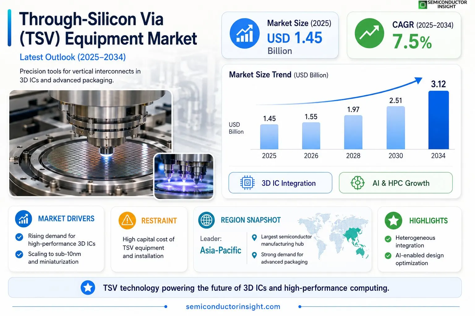
Global TSV equipment market size was valued at USD 1.45 billion in 2025. The market is projected to grow from USD 1.55 billion in 2025 to USD 3.12 billion by 2034, exhibiting a CAGR of 7.5% during the forecast period.
Through‑Silicon Via (TSV) equipment comprises precision wafer‑bonding tools, laser drilling systems, and wafer‑level packaging platforms that enable vertical electrical interconnections through silicon substrates, essential for advanced heterogeneous integration and high‑performance computing.The market is accelerating because semiconductor manufacturers are scaling toward sub‑10 nm nodes and demand for three‑dimensional ICs is surging. Furthermore, increased investment in AI accelerators and automotive electronics drives adoption of TSV technology. Key players such as Applied Materials, ASML Holding, Lam Research, and TSMC are expanding their portfolios through strategic partnerships and technology upgrades.
MARKET DRIVERS
Increasing Demand for High‑Performance 3D ICs
The rapid growth of smartphones, data‑center processors, and automotive electronics is pushing manufacturers toward three‑dimensional integration. Through‑Silicon Via (TSV) Equipment Market providers benefit from this shift as 3D ICs offer lower latency and higher bandwidth compared with traditional planar architectures. Recent industry forecasts indicate that 3D IC adoption could exceed 35% of total chip shipments by 2028, creating a sustained propulsion for TSV tooling sales.
Advancements in Miniaturization Technologies
Miniaturization pressures are compelling semiconductor fabs to replace wire‑bond interconnects with TSVs, which enable sub‑10‑micron interlayer connections. Through‑Silicon Via (TSV) Equipment Market players are responding with high‑precision laser drilling and atomic‑layer deposition solutions that reduce defect rates to below 0.5 % per wafer. These technical gains translate into higher yields and lower total cost of ownership for end‑users.
➤ “TSV adoption is projected to grow at a CAGR of 14 % through 2030, driven by the convergence of AI workloads and edge computing.”
In addition, strategic collaborations between equipment manufacturers and major foundries are accelerating technology transfer, shortening development cycles, and reinforcing confidence in the scalability of TSV processes across diverse product portfolios.
MARKET CHALLENGES
High Capital Expenditure for TSV Tooling
Acquiring a complete TSV linecomprising wafer thinning, via formation, and redistribution layers requires investments often exceeding $150 million. Smaller foundries struggle to finance such programs, resulting in a concentration of market share among a few large players and limiting broader technology diffusion.
Other Challenges
Process Integration Complexity
Integrating TSV steps into existing 200 mm or 300 mm fabs demands extensive re‑qualification of process flows. Variability in via fill quality and thermal management can cause yield penalties, compelling manufacturers to allocate additional engineering resources to mitigate risk.
MARKET RESTRAINTS
Limited Availability of Skilled Workforce
Advanced TSV processes require operators familiar with high‑resolution laser ablation, plasma‑enhanced chemical vapor deposition, and in‑situ metrology. The current talent pool falls short of demand, especially in emerging semiconductor hubs, which slows equipment installation timelines and raises operational costs.
MARKET OPPORTUNITIES
Emergence of AI‑Driven Design Tools
AI‑enabled layout optimization platforms are streamlining TSV placement, reducing the number of required vias by up to 20 % while maintaining signal integrity. This improvement lowers material consumption and accelerates time‑to‑market for new products, presenting a clear growth avenue for Through‑Silicon Via (TSV) Equipment Market vendors that integrate AI capabilities into their service offerings.
Through-Silicon Via (TSV) Equipment Market Trends
Sub‑10 nm Scaling Accelerates TSV Tool Adoption
Manufacturers targeting sub‑10 nm logic and memory nodes are increasingly dependent on vertical electrical interconnections to meet bandwidth and power‑efficiency goals. Precision wafer‑bonding tools, laser drilling systems, and wafer‑level packaging platforms have become essential for creating high‑density through‑silicon vias that support three‑dimensional integration. The shift toward heterogeneous integrationcombining logic, memory, and sensor functions in a single stackplaces pressure on equipment suppliers to deliver tighter alignment tolerances, reduced defectivity, and faster cycle times. As a result, production lines are upgrading legacy bonding stations with advanced in‑situ metrology and adopting high‑throughput laser drill heads to sustain yield growth while keeping fab footprints compact.
Other Trends
AI Accelerators and Automotive Electronics
The rise of artificial‑intelligence inference engines and safety‑critical automotive controllers is expanding the demand for high‑performance, stackable silicon solutions. AI accelerators benefit from TSV‑enabled interposers that minimize latency between compute dies, while automotive applications require robust thermal paths that TSV structures can provide. OEMs are collaborating with semiconductor vendors to qualify TSV‑based modules for stringent automotive reliability standards, prompting equipment makers to integrate temperature‑controlled processing stations and contamination‑free handling modules. These sector‑specific pressures are driving a parallel track of equipment specialization focused on low‑stress processing and accelerated test‑chip validation.
Strategic Portfolio Expansion by Leading Suppliers
Key industry playersincluding Applied Materials, ASML Holding, Lam Research, and TSMCare broadening their TSV equipment suites through strategic partnerships and technology upgrades. Collaboration with material‑science firms enables the introduction of novel dielectric liners that improve via reliability, while joint ventures with software providers embed predictive analytics into tool control loops. This ecosystem approach not only shortens time‑to‑market for next‑generation 3‑D ICs but also reduces total cost of ownership for customers by consolidating multiple process steps into integrated platforms. The cumulative effect is a more agile supply chain capable of responding to rapid design cycles in emerging high‑performance computing markets.
COMPETITIVE LANDSCAPEKey Industry Players
Through‑Silicon Via (TSV) Equipment Market Competitive Landscape
The TSV equipment segment is dominated by a handful of large, vertically integrated vendors that combine wafer‑bonding, laser‑drilling and wafer‑level packaging capabilities. Applied Materials leads with its comprehensive TSV bonding platforms that serve both memory and logic fabs, while ASML Holding leverages its lithography expertise to offer high‑precision laser drilling solutions for sub‑10 nm nodes. Lam Research’s TSV etch and deposition tools complement its strong presence in advanced node process equipment, reinforcing a market structure where a few multinational corporations command the majority of revenue and set technology roadmaps. TSMC, although primarily a fab, drives equipment adoption through internal development programs and strategic partnerships, further cementing the oligopolistic nature of the TSV ecosystem.Beyond the headline players, several niche and regionally focused firms contribute essential innovations that diversify the supply chain. Besi (BE Semiconductor Industries) supplies high‑throughput wafer‑level packaging equipment that enables cost‑effective TSV integration for automotive and IoT devices. Tokyo Electron offers specialized deposition tools that support three‑dimensional interconnect stacks. Samsung Electronics and Intel run in‑house TSV lines that stimulate demand for specialized bonding and inspection hardware from vendors such as Kulicke & Soffa and CVD Solutions. Emerging players like GlobalFoundries and NXP Semiconductors partner with equipment specialists to tailor TSV processes for custom ASICs, while ASE Technology Holding expands its packaging portfolio with advanced TSV test and reliability platforms.
List of Key Through-Silicon Via (TSV) Equipment Companies Profiled
- Applied Materials
- ASML Holding
- Lam Research
- TSMC
- Samsung Electronics
- Intel Corporation
- BE Semiconductor Industries (Besi)
- Tokyo Electron
- Kulicke & Soffa
- GlobalFoundries
- NXP Semiconductors
- ASE Technology Holding
- CVD Solutions
Segment Analysis:
| Segment Category | Sub-Segments | Key Insights |
| By Type |
|
Laser Drilling Systems – Provide precise, high‑aspect‑ratio via creation essential for fine‑pitch interconnects. – Enable rapid cycle times that align with aggressive fab schedules. – Offer flexibility across varied silicon thicknesses, supporting both memory and logic integration. |
| By Application |
|
High‑Performance Computing – Drives demand for ultra‑dense interconnects that TSV equipment uniquely supplies. – Benefits from the ability of TSV to reduce signal latency and power consumption in large‑scale processors. – Encourages co‑development of tooling that supports emerging heterogeneous integration approaches. |
| By End User |
|
Integrated Device Manufacturers – Favor TSV equipment that integrates seamlessly with existing wafer‑level processes. – Prioritize platforms that can be scaled across multiple product families without extensive re‑qualification. – Value supplier relationships that deliver consistent technology upgrades aligned with roadmap evolution. |
| By Process Stage |
|
Back‑End Packaging – Emerges as the primary arena where TSV equipment adds competitive advantage. – Provides the necessary precision to align vias after die stacking, crucial for 3‑D IC reliability. – Encourages equipment vendors to embed smart metrology that monitors via integrity in real‑time. |
| By Market Driver |
|
Demand for 3‑D ICs – Fuels investment in TSV equipment that can support increasingly complex stack heights. – Pushes suppliers to innovate on thermal management capabilities within drilling tools. – Shapes collaborative ecosystems where equipment makers work closely with design houses to optimize via patterns. |
Regional Analysis: North America
United States
The US is at the forefront of developing advanced packaging techniques that heavily rely on TSV technology to achieve greater functionality within smaller form factors. This includes 2.5D and 3D integration, crucial for enhancing chip performance.
The surging demand for AI and HPC applications in the US is directly fueling the need for high-performance chips incorporating TSV technology to meet computational requirements. This creates significant opportunities for TSV equipment suppliers.
Significant government funding allocated to semiconductor research and development in the US acts as a catalyst for innovation in TSV equipment and related technologies, further strengthening the domestic market.
The growing integration of sophisticated electronics within vehicles necessitates advanced packaging solutions utilizing TSV technology for enhanced performance and reliability, presenting a key growth area for the US market.
Europe
Europe represents a significant and steadily growing market for Through-Silicon Via (TSV) Equipment. Several European nations, particularly Germany, the United Kingdom, and the Netherlands, possess strong foundational capabilities in semiconductor design, manufacturing, and advanced materials, creating a fertile ground for TSV technology adoption. The automotive industry’s increasing focus on electric vehicles (EVs) and advanced driver-assistance systems (ADAS) is a key driver of demand, as TSV technology enables more efficient and powerful control units. Furthermore, the growing emphasis on energy efficiency and miniaturization in consumer electronics fuels the need for TSV-enabled chip designs. While the European market might not yet match the scale of the US or Asia-Pacific, it offers substantial potential for growth and is actively fostering innovation in this critical area.
Asia-Pacific
Asia-Pacific is poised to become the largest and fastest-growing market for Through-Silicon Via (TSV) Equipment. Driven by the massive expansion of the semiconductor industry in countries like China, Taiwan, and South Korea, the demand for TSV technology is surging. The proliferation of 5G infrastructure, the rapid adoption of AI and machine learning across various sectors, and the burgeoning demand for high-performance computing are all fueling this growth. Taiwan, with its dominance in semiconductor manufacturing, is a key market and innovation hub. China’s significant investments in its domestic semiconductor industry are further accelerating demand for TSV equipment. The region’s manufacturing prowess and strong industrial base provide a conducive environment for the widespread adoption of TSV technology across diverse applications.
South America
South America presents a relatively nascent but gradually expanding market for Through-Silicon Via (TSV) Equipment. The region’s semiconductor industry is still developing, with key players primarily focused on supporting local electronics manufacturing and telecommunications infrastructure. The increasing adoption of IoT devices, the growth of the automotive sector, and the expansion of data centers are contributing to a moderate increase in demand. While the overall market size remains smaller compared to other regions, the potential for growth is significant as the region continues to invest in technological advancements and strengthen its industrial capabilities. The focus is currently on cost-effective TSV solutions to cater to the evolving needs of the regional electronics ecosystem.
Middle East & Africa
The Middle East and Africa represent an emerging market for Through-Silicon Via (TSV) Equipment, with growth potential tied to infrastructure development and increasing adoption of technology across various sectors. The expansion of data centers in the region, driven by the growing demand for cloud services and digital transformation, is a key driver. Furthermore, investments in smart city initiatives, industrial automation, and the burgeoning automotive industry are contributing to a gradual increase in demand for advanced semiconductor packaging solutions, including TSV technology. While the current market size is relatively small, the long-term outlook is positive, particularly with continued infrastructure investments and economic growth across the region.
Report Scope
This market research report provides a comprehensive analysis of the Through-Silicon Via (TSV) Equipment Market , covering the forecast period 2026–2034. It offers detailed insights into market dynamics, technological advancements, competitive landscape, and key trends shaping the industry.
Key focus areas of the report include:
- Market Overview: The report begins with an overview outlining its current market scenario, key growth indicators, and industry transformation drivers. It discusses macroeconomic factors, demand–supply balance, regulatory landscape, and the strategic role of semiconductors in powering advancements across industries such as automotive, telecommunications, consumer electronics, and industrial automation.
- Market Size & Forecast: Historical data and future projections for revenue, unit shipments, and market value across major regions and segments.
- Segmentation Analysis: Detailed breakdown by product type, technology, application, and end-user industry to identify high-growth segments and investment opportunities.
- Regional Insights: Insights into market performance across North America, Europe, Asia-Pacific, Latin America, and the Middle East & Africa, including country-level analysis where relevant.
- Competitive Landscape: Profiles of leading market participants, including their product offerings, R&D focus, manufacturing capacity, pricing strategies, and recent developments such as mergers, acquisitions, and partnerships.
- Technology Trends & Innovation: Assessment of emerging technologies, integration of AI/IoT, semiconductor design trends, fabrication techniques, and evolving industry standards.
- Market Drivers & Restraints: Evaluation of factors driving market growth along with challenges, supply chain constraints, regulatory issues, and market-entry barriers.
- Stakeholder Insights: Insights for component suppliers, OEMs, system integrators, investors, and policymakers regarding the evolving ecosystem and strategic opportunities.
Primary and secondary research methods are employed, including interviews with industry experts, data from verified sources, and real-time market intelligence to ensure the accuracy and reliability of the insights presented.
FREQUENTLY ASKED QUESTIONS:
What is the current market size of Through-Silicon Via (TSV) Equipment Market?
-> Through-Silicon Via (TSV) Equipment Market was valued at USD 1.45 billion in 2025 and is expected to reach USD 3.12 billion by 2034, reflecting a CAGR of 7.5% during the forecast period.
Which key companies operate in Through-Silicon Via (TSV) Equipment Market?
-> Key players include Applied Materials, ASML Holding, Lam Research, and TSMC, among others.
What are the key growth drivers?
-> Key growth drivers include scaling to sub‑10 nm nodes, rising demand for three‑dimensional ICs, increased investment in AI accelerators, and growth in automotive electronics.
Which region dominates the market?
-> Asia‑Pacific leads the market due to the concentration of semiconductor fabs and strong demand for advanced packaging solutions, while North America and Europe also show significant activity.
What are the emerging trends?
-> Emerging trends include heterogeneous integration using TSVs, AI‑enabled design optimization, and expanding use of TSVs in high‑performance computing and automotive applications.

Get Sample Report PDF for Exclusive Insights
Report Sample Includes
- Table of Contents
- List of Tables & Figures
- Charts, Research Methodology, and more...
 Download Sample Report PDF