Advanced Packaging for AI Chip Market Insights
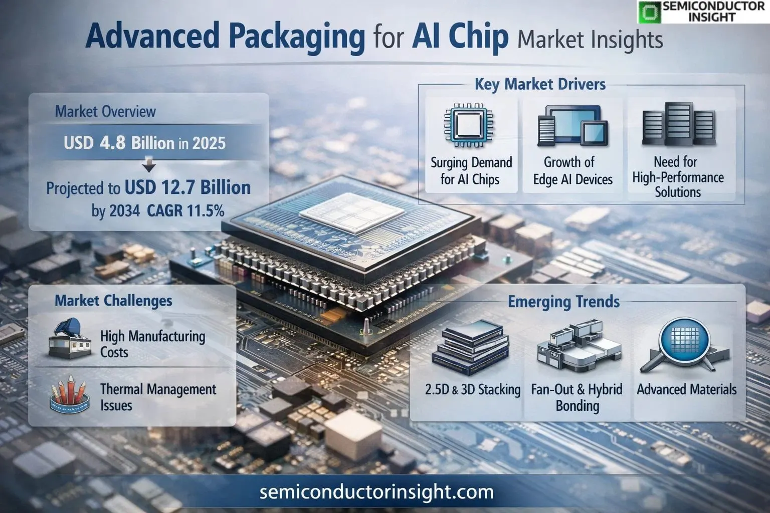
Global Advanced Packaging for AI Chip market size was valued at USD 4.8 billion in 2025. The market is projected to grow from USD 5.3 billion in 2026 to USD 12.7 billion by 2034, exhibiting a CAGR of 11.5% during the forecast period.
Advanced packaging technologies for AI chips are critical solutions designed to enhance performance, power efficiency, and thermal management in artificial intelligence applications. These technologies include 2.5D CoWoS (Chip-on-Wafer-on-Substrate), 3D stacking, and other innovative approaches that enable higher interconnect density and improved signal integrity for AI processors.
The market growth is driven by increasing demand for high-performance computing in AI workloads, the proliferation of edge AI devices, and the need for energy-efficient chip designs. Leading semiconductor companies such as TSMC, Samsung, and Intel are investing heavily in advanced packaging solutions to address the challenges of scaling traditional Moore’s Law approaches. For instance, TSMC’s CoWoS technology has become a key enabler for NVIDIA’s latest AI accelerators, demonstrating how packaging innovations can unlock new levels of performance.
MARKET DRIVERS
Rising Demand for AI Acceleration Hardware
Global AI chip market is projected to grow at 35% CAGR through 2030, driving advanced packaging for AI chips adoption. AI workloads require high-speed interconnects and thermal efficiency, which traditional packaging cannot deliver. This has led to increased R&D investments exceeding $4 billion in 2023 for AI-optimized packaging solutions.
Performance Requirements for Edge AI
Edge AI deployments grew by 62% in 2023, creating demand for compact yet powerful advanced packaging formats like 2.5D and 3D IC. These technologies provide 40-50% better power efficiency compared to conventional packages, critical for battery-operated devices.
The advanced packaging for AI chip market is expected to reach $12.7 billion by 2027, with heterogeneous integration being the fastest-growing segment at 48% CAGR.
Leading semiconductor firms are transitioning to chiplet-based designs, with over 75% of new AI processor designs incorporating advanced packaging techniques for improved yield and scalability.
MARKET CHALLENGES
High Development and Manufacturing Costs
Setting up advanced packaging facilities requires capital expenditures exceeding $1 billion, creating high barriers to entry. The complex assembly processes for AI chip packaging result in yields below 80% for some cutting-edge nodes, increasing per-unit costs.
Other Challenges
Thermal Management Complexities
AI chips packaged with 3D stacking technology face thermal densities above 100W/cm², requiring expensive cooling solutions that add 15-20% to system costs.
Supply Chain Constraints
Specialized substrates for AI chip packaging face 6-9 month lead times, with only three suppliers controlling 85% of the advanced substrate market.
MARKET RESTRAINTS
Technical Limitations in Package Scaling
While advanced packaging for AI chips enables continued performance gains, signal integrity challenges limit interconnect densities beyond 100μm pitch. Current materials struggle with warpage control at these scales, restricting further miniaturization of AI processor packages.
MARKET OPPORTUNITIES
Emerging Fan-Out and Hybrid Bonding Technologies
The advanced packaging for AI chip market is witnessing breakthroughs in fan-out wafer-level packaging (FOWLP) with adoption rates growing 32% annually. Hybrid bonding techniques are enabling sub-10μm interconnect pitches, crucial for next-gen AI accelerator packaging designs.
Advanced Packaging for AI Chip Market Trends
Shift Toward Heterogeneous Integration
The Advanced Packaging for AI Chip Market is witnessing a major shift toward heterogeneous integration technologies. Leading foundries like TSMC and Intel are adopting 2.5D CoWoS and 3D stacking to address the increasing performance demands of AI workloads. This integration allows combining logic, memory, and I/O components in single packages, improving bandwidth and reducing latency.
Other Trends
Memory-Centric Packaging Gains Traction
Advanced packaging solutions are increasingly focusing on memory integration to overcome bandwidth limitations in AI chips. Technologies like HBM (High Bandwidth Memory) integrated with GPUs through silicon interposers are becoming critical for AI training applications. Major memory manufacturers SK Hynix and Micron are developing specialized packaging for AI memory solutions.
Material Innovations in Advanced Packaging
The industry is seeing breakthroughs in thermally conductive materials and low-loss dielectrics to address thermal management challenges in AI chip packaging. Companies like Amkor Technology and ASE Technology are developing new substrate materials that can withstand higher power densities while maintaining signal integrity for AI processor packages.
Regional Manufacturing Ecosystems Evolve
Geopolitical factors are driving diversification in Advanced Packaging for AI Chip manufacturing locations. While Taiwan and South Korea currently dominate, new packaging facilities are emerging in the U.S., China, and Southeast Asia to create more resilient supply chains for critical AI hardware components.
Standardization Efforts Intensify
The industry is moving toward standardized interfaces and packaging specifications to enable broader adoption of advanced packaging solutions. Consortiums involving TSMC, Intel, and Samsung are working on common standards to reduce development costs and accelerate time-to-market for AI chip packaging technologies.
COMPETITIVE LANDSCAPE
Key Industry Players
TSMC Dominates Advanced Packaging for AI Chips with 40% Market Share
Taiwan Semiconductor Manufacturing Company (TSMC) leads the advanced packaging for AI chips market with its proprietary CoWoS (Chip-on-Wafer-on-Substrate) technology, capturing approximately 40% of global revenue. The market is characterized by strategic partnerships between foundries and memory providers, with Samsung, Intel, and SK Hynix emerging as formidable competitors through vertical integration strategies. Niche players like ASE Technology and Amkor Technology are gaining traction through specialized packaging solutions for high-performance computing applications.
Chinese manufacturers such as JCET Group and Tongfu Microelectronics are rapidly expanding their advanced packaging capabilities to meet domestic AI chip demand. Meanwhile, Intel’s Foveros 3D stacking technology and Samsung’s X-Cube solutions are driving innovation in heterogeneous integration for AI processors. The competitive landscape remains dynamic with ongoing R&D investments exceeding $2 billion annually among top players to develop next-generation packaging solutions.
List of Key Advanced Packaging for AI Chip Companies Profiled
- Taiwan Semiconductor Manufacturing Company (TSMC)
- Samsung Electronics
- Intel Corporation
- SK Hynix
- Micron Technology
- ASE Technology Holding
- Amkor Technology
- JCET Group
- Tongfu Microelectronics
- Powertech Technology
- Silicon Precision Industries (SPIL)
- Chipbond Technology
- STATS ChipPAC
- NEPES Corporation
- HT-Tech
Segment Analysis:
| Segment Category | Sub-Segments | Key Insights |
| By Type |
|
2.5D CoWoS emerges as the dominant packaging technology with:
|
| By Application |
|
AI Accelerators drive maximum demand due to:
|
| By End User |
|
Cloud Service Providers dominate the market with:
|
| By Packaging Material |
|
Silicon Interposers show significant growth potential due to:
|
| By Technology Provider |
|
Foundry-led Solutions lead the market with:
|
Regional Analysis: Advanced Packaging for AI Chip Market
Asia-Pacific
Taiwan controls over 50% of global advanced packaging capacity with TSMC’s CoWoS and InFO technologies setting standards for AI chip packaging. Local OSATs provide comprehensive solutions spanning fan-out to chiplet integration.
South Korean firms excel in high-bandwidth memory stacking crucial for AI processors. Their expertise in TSV (Through-Silicon Via) technology enables 3D packaging solutions optimizing performance for machine learning workloads.
China is rapidly building advanced packaging capabilities through acquisitions and domestic R&D. Major Chinese foundries are implementing sophisticated packaging architectures to support indigenous AI chip development initiatives.
Japanese suppliers provide critical materials and equipment for fan-out wafer-level packaging. Their specialty substrates and thermal interface materials address AI chips’ power density and heat dissipation challenges.
North America
North America remains innovation hub for advanced packaging techniques, with leading AI chip designers driving packaging requirements. The region focuses on chiplets architecture and ultra-high-density interconnects for AI workloads. Major US semiconductor companies collaborate with Asian partners on next-generation packaging while maintaining R&D centers for proprietary technologies. Silicon Valley’s ecosystem fosters packaging start-ups specializing in photonic integration and quantum computing packaging solutions.
Europe
European advanced packaging efforts concentrate on automotive and industrial AI applications. IMEC in Belgium leads research into 3D system integration and thermal management solutions. The region shows growing expertise in wafer-level packaging for edge AI chips, with German and French equipment suppliers developing specialized tools for heterogeneous integration packaging processes.
Middle East & Africa
The region is emerging as potential location for advanced packaging facilities with strategic investments in semiconductor infrastructure. Israel contributes packaging IP for specialized AI accelerators, while Gulf nations are establishing technology hubs with packaging capabilities as part of broader digital transformation initiatives.
South America
South America’s advanced packaging market is nascent but growing, focused mainly on test and assembly services for AI chips. Brazil and Mexico are developing technical talent pools and infrastructure to participate in global semiconductor packaging value chains, particularly for automotive and consumer electronics applications.
Report Scope
This market research report provides a comprehensive analysis of the Advanced Packaging for AI Chip Market, covering the forecast period 2025–2034. It offers detailed insights into market dynamics, technological advancements, competitive landscape, and key trends shaping the industry.
Key focus areas of the report include:
- Market Overview: The report begins with an overview outlining its current market scenario, key growth indicators, and industry transformation drivers. It discusses macroeconomic factors, demand–supply balance, regulatory landscape, and the strategic role of semiconductors in powering advancements across industries such as automotive, telecommunications, consumer electronics, and industrial automation.
- Market Size & Forecast: Historical data and future projections for revenue, unit shipments, and market value across major regions and segments.
- Segmentation Analysis: Detailed breakdown by product type, technology, application, and end-user industry to identify high-growth segments and investment opportunities.
- Regional Insights: Insights into market performance across North America, Europe, Asia-Pacific, Latin America, and the Middle East & Africa, including country-level analysis where relevant.
- Competitive Landscape: Profiles of leading market participants, including their product offerings, R&D focus, manufacturing capacity, pricing strategies, and recent developments such as mergers, acquisitions, and partnerships.
- Technology Trends & Innovation: Assessment of emerging technologies, integration of AI/IoT, semiconductor design trends, fabrication techniques, and evolving industry standards.
- Market Drivers & Restraints: Evaluation of factors driving market growth along with challenges, supply chain constraints, regulatory issues, and market-entry barriers.
- Stakeholder Insights: Insights for component suppliers, OEMs, system integrators, investors, and policymakers regarding the evolving ecosystem and strategic opportunities.
Primary and secondary research methods are employed, including interviews with industry experts, data from verified sources, and real-time market intelligence to ensure the accuracy and reliability of the insights presented.
FREQUENTLY ASKED QUESTIONS:
What is the current market size of Advanced Packaging for AI Chip Market?
-> The Advanced Packaging for AI Chip Market was valued at USD 4.8 billion in 2025 and is projected to reach USD 12.7 billion by 2034
Which key companies operate in Advanced Packaging for AI Chip Market?
-> Key players include TSMC, Micron, SK Hynix, Samsung, Intel, ASE Technology, and Amkor Technology, among others.
What are the key growth drivers?
-> Key growth drivers include increasing demand for AI chips, advancements in semiconductor packaging technologies, and rising applications in data centers and edge computing.
Which region dominates the market?
-> Asia is the fastest-growing region, with China expected to reach USD million by 2034.
What are the emerging trends?
-> Emerging trends include 2.5D CoWoS packaging, 3D stacking technologies, and integration of advanced materials for enhanced thermal management.
Get Sample Report PDF for Exclusive Insights
Report Sample Includes
- Table of Contents
- List of Tables & Figures
- Charts, Research Methodology, and more...


