
Small Size Semiconductor Wafer Market Insights
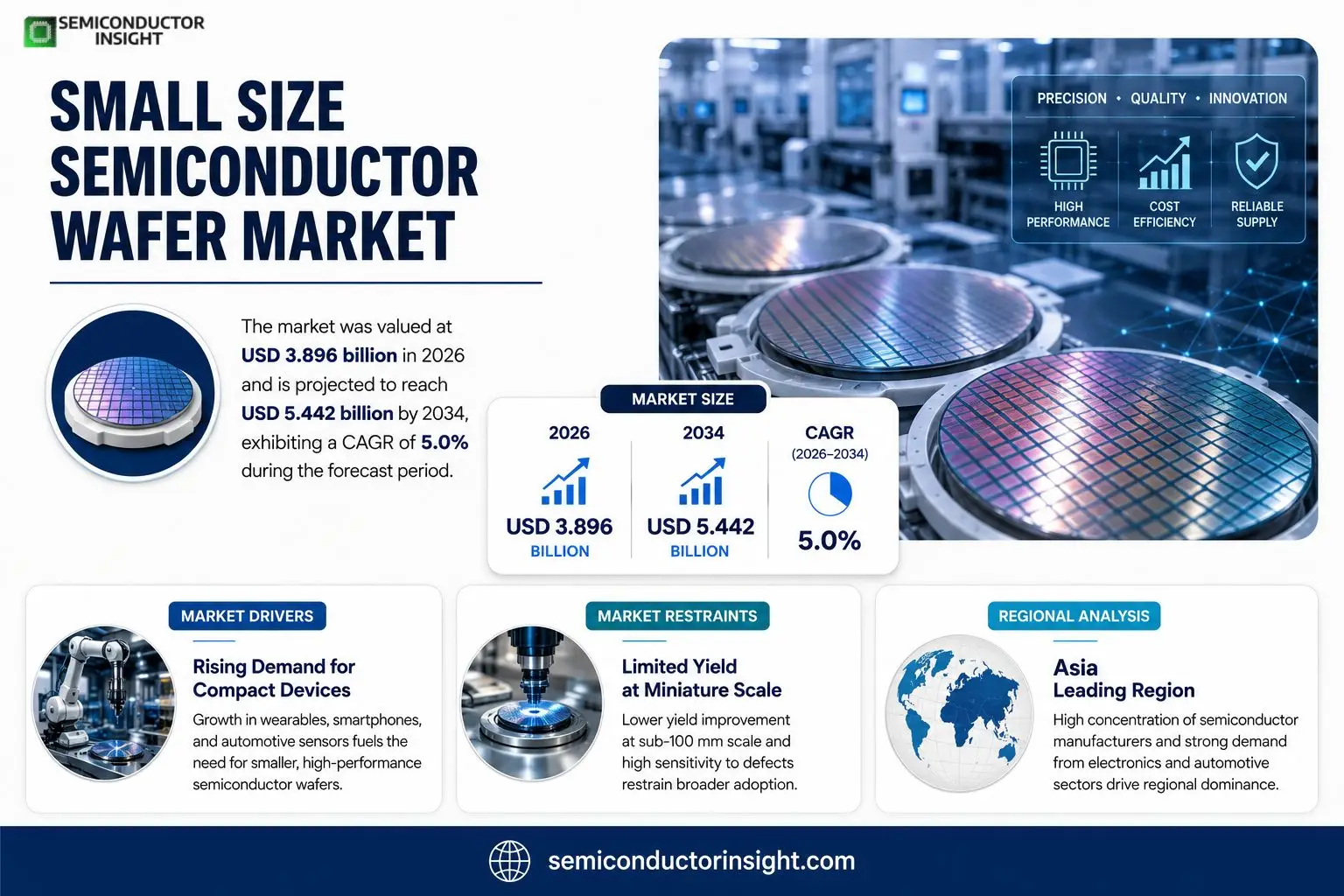
Small Size Semiconductor Wafer market was valued at USD 3.896 billion in 2026 and is projected to reach USD 5.442 billion by 2034 exhibiting a CAGR of 5.0% during the forecast period.
Small Size Semiconductor Wafers are silicon substrates typically sized at 8‑inch, 6‑inch, or 3‑5‑inch diameters. They act as the foundational platform for a broad spectrum of semiconductor devicesfrom smartphones and home appliances to automotive power modules, AI processors, and IoT sensorsby providing a precisely engineered crystalline base for integrated circuit fabrication.The market expands because manufacturers are shifting toward cost‑effective small diameters for legacy process nodes while demand from automotive power devices and sensor applications sustains volume growth. Recent capacity expansions by leading suppliers such as Shin‑Etsu Chemical, SUMCO, and GlobalWafers signal confidence in continued demand across consumer electronics and emerging AI workloads.
MARKET DRIVERS
Increasing Demand for Compact Devices
The proliferation of wearables, ultra‑thin smartphones, and miniaturized automotive sensors has forced OEMs to shrink the silicon footprint of their products. Small Size Semiconductor Wafer Market entrants that can deliver consistent performance at reduced dimensions are therefore gaining preferential treatment in design road‑maps. This shift is less about novelty and more about meeting the physical constraints imposed by next‑generation form factors.
Advances in Lithography for Small Wafer Sizes
Recent upgrades to extreme‑ultraviolet (EUV) and immersion lithography tools have lowered the minimum viable feature size, making it economically viable to process wafers under 100 mm. Manufacturers that adopt these tools early can achieve cost per die reductions of up to 15 %, a margin that directly influences pricing strategies for end‑product makers.
➤ Analysts observe that firms with integrated process control loops are better positioned to translate lithographic gains into higher throughput on small wafers.
Beyond technology, the strategic push by semiconductor giants to diversify their product portfolios has spurred investment in niche fabs dedicated to small‑size production. This capital inflow translates into faster time‑to‑market for specialized chips, reinforcing the upward momentum of the market.
MARKET CHALLENGES
Cost Sensitivity of Small‑size Production
Operating a fab that handles sub‑100 mm wafers demands a distinct set of tooling and clean‑room standards, which often lack the economies of scale enjoyed by larger‑diameter lines. Even modest fluctuations in raw‑material prices can erode profit margins, prompting manufacturers to adopt stringent cost‑management protocols.
Other Challenges
Supply Chain Constraints
The limited number of qualified equipment suppliers for miniature wafer processing creates bottlenecks, especially when demand spikes for specialized devices. Lead times for critical components such as photo‑masks and metrology tools have expanded, forcing planners to hold larger safety stocks.In addition, the talent pool skilled in handling small‑size lithography is relatively shallow. Companies that fail to invest in targeted training programs may encounter productivity lags, further amplifying the cost pressures described above.
MARKET RESTRAINTS
Limited Yield Improvement at Miniature Scale
Yield curves for wafers below 100 mm often flatten earlier than those for larger substrates, because defect densities become proportionally more impactful. A single particle can render an entire die unusable, which diminishes the overall cost advantage of downsizing. Until defect‑mitigation technologies mature, this yield ceiling will restrain broader adoption.
MARKET OPPORTUNITIES
Emerging Applications in IoT Edge Computing
Edge devices that process data locally require ultra‑low power envelopes and minimal silicon area. Small Size Semiconductor Wafer Market players that can combine high integration density with low leakage are uniquely positioned to capture contracts from industrial IoT platforms, smart‑city sensors, and medical wearables. The convergence of 5G connectivity and AI inference at the edge amplifies this opportunity, encouraging firms to tailor their process lines toward niche, high‑value segments.
Small Size Semiconductor Wafer Market Trends
Shift Toward Integrated Small‑Diameter Wafer Lines
Small Size Semiconductor Wafer Market is seeing a noticeable move away from isolated fab equipment toward tightly coupled production lines that handle 8‑inch, 6‑inch and sub‑5‑inch wafers in a single flow. Manufacturers cite higher yield consistency and lower scrap rates as primary incentives. By consolidating lithography, etch and metrology stages within a common clean‑room footprint, suppliers can reduce change‑over time between product families such as power ICs and sensor dice. This operational tightness also eases capacity planning for customers that run mixed‑technology portfolios, because the same wafer size can serve both legacy analog devices and newer AI‑edge chips. The net effect is a modest compression of lead times and a shift in capital budgeting from multiple discrete tools to more versatile, modular platforms.
Other Trends
Consolidation Among Top Ten Suppliers
Analysis of Small Size Semiconductor Wafer Market reveals that the ten leading producers together command roughly 88 % of global output. This concentration stems from a series of strategic acquisitions and joint‑venture arrangements that have aligned capacity with the steep increase in wafer demand from automotive‑grade logic and power applications. Companies such as Shin‑Etsu Chemical, SUMCO and GlobalWafers have leveraged scale to negotiate more favorable raw‑silicon pricing, while also investing in high‑purity crystal growth facilities that smaller entrants cannot readily match. The resulting barrier to entry discourages new competitors and encourages incumbent firms to focus on differentiation through specialty coatings and low‑defect process windows.
Emerging Applications in Edge AI and Automotive Sensors
Beyond traditional consumer electronics, Small Size Semiconductor Wafer Market is being reshaped by a surge in edge‑AI processors and advanced driver‑assistance sensors. These applications require wafer platforms that balance cost efficiency with the ability to host dense transistor architectures. Smaller diameters allow fab lines to achieve tighter thermal control, which is critical for the high‑frequency operation of modern analog‑digital mixed‑signal blocks. As vehicle manufacturers pursue higher levels of autonomy, the demand for compact, high‑performance wafers is expected to rise, prompting suppliers to expand capacity for 5‑inch and 4‑inch formats that cater specifically to sensor‑centric designs. This trend is prompting several fab owners to re‑tool existing 8‑inch lines for mixed‑size runs, thereby preserving flexibility while addressing the distinct needs of the automotive supply chain.
COMPETITIVE LANDSCAPE
Key Industry Players
Small Size Semiconductor Wafer: Competitive Dynamics in 2026‑2031
Shin‑Etsu Chemical continues to command the largest share of the small‑size silicon wafer arena, leveraging a vertically integrated supply chain that couples high‑purity crystal growth with advanced polishing technologies. Its ability to secure long‑term contracts with major IC fabs gives it pricing leverage and ensures a steady flow of 8‑inch and 6‑inch wafers to logic and analog manufacturers. The company’s focus on yield improvement and defect reduction has set an industry benchmark, compelling rivals to invest heavily in similar capabilities. As the market edges toward a valuation above US$5 billion by the early 2030s, Shin‑Etsu’s scale and R&D intensity position it as the de‑facto standard‑setter for quality and volume.A cohort of specialized firms rounds out the competitive set. SUMCO and GlobalWafers have expanded capacity in 200‑mm formats, targeting automotive and power‑device segments where wafer thickness and uniformity are paramount. Siltronic AG differentiates through its high‑performance epitaxial products for sensor applications, while SK Siltron emphasizes cost‑effective production for consumer electronics. Regional players such as National Silicon Industry Group, Zhonghuan Advanced Semiconductor Materials, and Zhejiang Jinruihong Technologies focus on serving Chinese fabs, benefiting from proximity to burgeoning domestic demand. Meanwhile, niche innovators like GRINM Semiconductor Materials and Soitec introduce engineered substrates for advanced packaging, carving out pockets of differentiated revenue despite their smaller overall footprints.
List of Key Small Size Semiconductor Wafer Companies Profiled
- Shin‑Etsu Chemical
- SUMCO
- GlobalWafers
- Siltronic AG
- SK Siltron
- National Silicon Industry Group (NSIG)
- Zhonghuan Advanced Semiconductor Materials
- Zhejiang Jinruihong Technologies
- Hangzhou Lion Microelectronics
- GRINM Semiconductor Materials
- Soitec
- Shanghai Advanced Silicon Technology (AST)
- XiAn ESWIN Technology Group
- Hebei Puxing Electronic Technology
- Nanjing Guosheng Electronics
Segment Analysis:
| Segment Category | Sub-Segments | Key Insights |
| By Type |
|
Leading Segment
|
| By Application |
|
Leading Segment
|
| By End User |
|
Leading Segment
|
| By Technology |
|
Leading Segment
|
| By Market Driver |
|
Leading Segment
|
Regional Analysis: Small Size Semiconductor Wafer Market
North America
Leading wafer suppliers are forming strategic alliances with equipment manufacturers to streamline the procurement of high‑precision polishing stations, thereby reducing lead times for small‑size rolls. This collaboration reflects a realistic response to the fragile capacity constraints that have emerged as demand for compact chips tightens.
Chip designers in the United States and Canada are embedding advanced patterning techniques early in the product lifecycle, which compels fab operators to adapt process modules for 100‑mm and 150‑mm wafers. The ripple effect narrows the gap between design intent and manufacturability.
A robust pipeline of wafer‑process engineers graduating from specialized programs sustains the region’s capacity to iterate on thin‑film deposition and etch chemistries, ensuring that capacity expansions are underpinned by skilled labor.
Recent revisions to export‑control statutes create a more predictable environment for cross‑border equipment sales, allowing fab owners to commit to longer‑term capital plans without fearing abrupt policy reversals.
Europe
European manufacturers are exploiting Small Size Semiconductor Wafer Market to reinforce their position in precision‑sensor applications, particularly within the automotive safety sector. Collaborative clusters in Germany and the Netherlands integrate wafer‑scale packaging with high‑frequency RF front‑ends, fostering a feedback loop that accelerates material‑selection decisions. Sustainability mandates are also influencing wafer‑handling protocols, prompting a shift toward water‑conserving cleaning chemistries that align with broader corporate ESG goals.
Asia‑Pacific
The Asia‑Pacific region, anchored by Taiwan and South Korea, channels its deep foundry expertise into sub‑150 mm production lines that feed a burgeoning market for wearable health monitors. Local governments incentivize equipment upgrades that enhance yield stability on smaller substrates, while contract manufacturers leverage their scale to offer cost‑effective turn‑key solutions for emerging startups seeking rapid market entry.
South America
In South America, Brazil’s semiconductor initiatives are still nascent, yet the demand for compact power‑management chips in renewable‑energy projects has sparked interest in small‑size wafers. Partnerships between regional universities and multinational fabs aim to develop a localized knowledge base, which could lower dependence on imported components and create a modest domestic supply chain.
Middle East & Africa
The Middle East & Africa segment remains at an exploratory stage, with Saudi Arabia and Israel piloting pilot lines that test the feasibility of miniaturized wafer processes for defense‑grade electronics. While capital allocation is cautious, the strategic imperative to diversify beyond oil‑centric economies is driving early‑stage investments in semiconductor education and modest fab upgrades.
Report Scope
This market research report provides a comprehensive analysis of the Small Size Semiconductor Wafer Market , covering the forecast period 2026–2034. It offers detailed insights into market dynamics, technological advancements, competitive landscape, and key trends shaping the industry.
Key focus areas of the report include:
- Market Overview: The report begins with an overview outlining its current market scenario, key growth indicators, and industry transformation drivers. It discusses macroeconomic factors, demand–supply balance, regulatory landscape, and the strategic role of semiconductors in powering advancements across industries such as automotive, telecommunications, consumer electronics, and industrial automation.
- Market Size & Forecast: Historical data and future projections for revenue, unit shipments, and market value across major regions and segments.
- Segmentation Analysis: Detailed breakdown by product type, technology, application, and end-user industry to identify high-growth segments and investment opportunities.
- Regional Insights: Insights into market performance across North America, Europe, Asia-Pacific, Latin America, and the Middle East & Africa, including country-level analysis where relevant.
- Competitive Landscape: Profiles of leading market participants, including their product offerings, R&D focus, manufacturing capacity, pricing strategies, and recent developments such as mergers, acquisitions, and partnerships.
- Technology Trends & Innovation: Assessment of emerging technologies, integration of AI/IoT, semiconductor design trends, fabrication techniques, and evolving industry standards.
- Market Drivers & Restraints: Evaluation of factors driving market growth along with challenges, supply chain constraints, regulatory issues, and market-entry barriers.
- Stakeholder Insights: Insights for component suppliers, OEMs, system integrators, investors, and policymakers regarding the evolving ecosystem and strategic opportunities.
Primary and secondary research methods are employed, including interviews with industry experts, data from verified sources, and real-time market intelligence to ensure the accuracy and reliability of the insights presented.
FREQUENTLY ASKED QUESTIONS:
What is the current market size of Small Size Semiconductor Wafer Market?
-> Small Size Semiconductor Wafer Market was valued at USD 3,896 million in 2026 and is expected to reach USD 5,442 million by 2034 growing at a CAGR of 5.0% during the forecast period.
Which key companies operate in Small Size Semiconductor Wafer Market?
-> Key players include Shin-Etsu Chemical, SUMCO, GlobalWafers, SK Siltron, Siltronic AG, FST Corporation, National Silicon Industry Group (NSIG), Zhonghuan Advanced Semiconductor Materials, Wafer Works Corporation, Zhejiang Jinruihong Technologies, and Hangzhou Semiconductor Wafer (CCMC).
What are the key growth drivers?
-> Key growth drivers include rising demand for smartphones, home appliances, and automobiles, coupled with the rapid expansion of AI and IoT applications that require advanced semiconductor substrates.
Which region dominates the market?
-> Asia dominates Small Size Semiconductor Wafer Market, driven by a high concentration of manufacturers and strong demand from electronics and automotive sectors.
What are the emerging trends?
-> Emerging trends include increased adoption of 8‑inch wafers, growth of AI/IoT‑driven applications, and accelerated development of 200 mm wafer fabrication capabilities.
Get Sample Report PDF for Exclusive Insights
Report Sample Includes
- Table of Contents
- List of Tables & Figures
- Charts, Research Methodology, and more...
 Download Sample Report PDF



