
Silicon on Insulator Market Insights
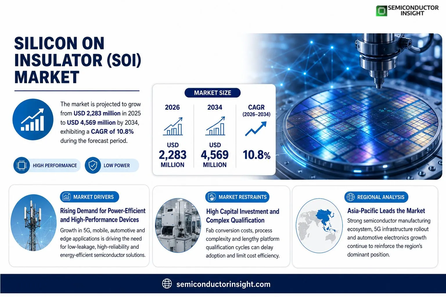
Silicon on Insulator market size was valued at USD 2,283 million in 2025 and expands to USD 4,569 million by 2034, reflecting a CAGR of 10.8% over the forecast period.
A silicon‑on‑insulator (SOI) wafer consists of a silicon handle substrate, an insulating buried‑oxide layer and a thin monocrystalline silicon device layer where transistors are formed. By electrically isolating devices from the bulk silicon, SOI reduces parasitic capacitance and substrate coupling, which improves signal integrity, suppresses latch‑up, lowers leakage and enhances robustness under high‑frequency, low‑voltage and harsh operating conditions.Demand is amplified by ongoing connectivity upgrades and the pressure for power‑efficient designs across semiconductor supply chains. As cellular and Wi‑Fi standards move toward higher frequencies and more bands, RF front‑end modules require substrates that can meet tighter linearity and loss budgetsconditions where SOI’s engineered isolation delivers measurable benefits. Simultaneously, edge computing, automotive and industrial applications prioritize low‑voltage operation and reliable performance, further encouraging adoption of SOI platforms despite cyclical demand swings and the need for coordinated qualification across foundry processes.
MARKET DRIVERS
Rising Power‑Efficiency Requirements in Mobile and Edge Devices
The relentless push for longer battery life has forced OEMs to look beyond conventional bulk silicon. Silicon on Insulator (SOI) wafers reduce junction capacitance, translating into lower dynamic power consumption. Recent product launches from flagship smartphones illustrate how manufacturers are leveraging this advantage to differentiate performance while keeping thermal budgets modest.
Expansion of 5G Infrastructure and Data‑Center Accelerators
5G base stations and high‑performance compute nodes rely heavily on radio‑frequency front‑ends and ASICs that demand superior signal integrity. SOI substrates provide the isolation needed for mixed‑signal circuits, reducing cross‑talk and enabling tighter integration of RF and digital blocks. Analysts observe that a sizable share of new 5G radio modules now incorporate SOI technology.
➤ “Adoption of SOI in the RF front‑end has cut power draw by up to 30 % for comparable designs,” notes a senior design engineer at a leading chipset supplier.
Beyond telecom, the automotive sector is embracing autonomous‑driving platforms that require low‑latency processing under stringent reliability standards. By mitigating latch‑up risks, SOI chips improve yield on safety‑critical modules, encouraging automakers to qualify more designs on this platform.
MARKET CHALLENGES
High Capital Expenditure for Fab Conversion
Transitioning a mature silicon fab to accommodate SOI processing imposes a sizable upfront cost, often exceeding $200 million for equipment upgrades and clean‑room modifications. Smaller foundries, which lack deep pockets, may hesitate to make such an investment, limiting the supply base for niche customers.
Other Challenges
Process Complexity
The additional bonding and layer‑transfer steps introduce greater variability. Manufacturers must implement tighter process controls, which can extend cycle times and elevate per‑wafer pricing relative to standard bulk silicon.
MARKET RESTRAINTS
Limited Design‑Tool Ecosystem
Although major EDA vendors have added SOI support, many legacy libraries still target bulk silicon. Design teams often need to rewrite critical blocks or validate custom models, which adds schedule risk and can deter early adoption for cost‑sensitive projects.
MARKET OPPORTUNITIES
Emerging Applications in Quantum‑Computing Interfaces
Quantum processors require ultra‑low‑noise control electronics. The isolation properties of SOI wafers make them suitable for cryogenic amplifiers and read‑out circuits, opening a new revenue stream as research labs transition to commercial prototypes. Companies that pre‑position SOI capability can capture early contracts in this nascent field.
Silicon on Insulator Market Trends
Increasing Adoption of RF and mmWave Substrates
The evolution of wireless standards has pushed front‑end modules toward higher frequencies and tighter linearity budgets. Engineers are turning to engineered silicon substrates because the buried oxide layer cuts parasitic capacitance, which translates directly into lower insertion loss and improved signal‑to‑noise ratios. Recent shipments of 4.5‑6.5 million pieces illustrate that manufacturers have already scaled production to meet carrier‑grade requirements. The price range of $300‑$650 per wafer reflects the premium placed on finer device‑layer thicknesses and larger diameters, yet the cost premium is justified by the yield benefits observed in high‑frequency fabs. As a result, design houses are embedding these wafers into reference designs, shortening time‑to‑market for multi‑band phones and IoT gateways.
Other Trends
Supply‑Chain Constraints and Qualification Timelines
Despite the evident technical advantages, the market remains sensitive to the cyclical nature of consumer electronics. Short‑run demand spikes can outpace the ability of SOI fabs to allocate capacity, especially when new device‑layer specifications are introduced. In parallel, customers must navigate a multi‑step qualification process that involves foundry PDKs, library support, and reliability testing. This extended onboarding often creates a lag between wafer availability and volume orders, prompting suppliers to maintain a modest inventory buffer. The net effect is a period of constrained supply that can influence pricing dynamics and incentivize early engagement between wafer producers and chipset designers.
Automotive and Edge Computing Fuel Low‑Power Platforms
Industrial controllers and automotive electronic control units are increasingly required to operate below 1 V while delivering high reliability over wide temperature ranges. The insulating layer of SOI wafers suppresses latch‑up and curtails off‑state leakage, allowing designers to meet stringent power budgets without resorting to complex body‑bias schemes. Moreover, the robustness of the substrate under harsh environments aligns with the reliability specifications of safety‑critical applications. As vehicle electrification accelerates and edge nodes proliferate in factories, the demand for substrates that combine low leakage with mechanical resilience is becoming a decisive factor in component selection, encouraging a steady shift toward engineered silicon solutions.
COMPETITIVE LANDSCAPE
Key Industry Players
Competitive Positioning and Strategic Moves in the SOI Wafer Market
Soitec continues to dominate the silicon‑on‑insulator (SOI) wafer arena, leveraging its mature bulk‑production line and a diversified product portfolio that spans 200 mm and 300 mm formats for RF, low‑power and power‑device segments. Its ability to tailor buried‑oxide thickness and device‑layer doping has secured long‑term contracts with major foundries, allowing the company to sustain double‑digit revenue growth despite cyclic demand in consumer electronics. The firm’s recent investment in a 300 mm pilot line reflects a strategic push to capture larger‑volume automotive and edge‑computing orders, where cost‑per‑wafer pressure is intensifying.Beyond Soitec, a cluster of specialists and integrated device manufacturers are expanding the competitive mix. Shin‑Etsu Handotai and Sumitomo Electric provide high‑precision SOI wafers for niche RF and millimeter‑wave applications, often commanding premium pricing for ultra‑thin BOX layers. FOUNDRIES and Intel have internal SOI capabilities, using them to differentiate core products such as 22 nm FDSOI platforms. Samsung Electronics recently announced a joint venture with Soitec to co‑develop 300 mm wafers targeting 5G front‑ends. European players including STMicroelectronics and Infineon Technologies rely on external suppliers but are actively shaping specification roadmaps to support automotive safety and industrial IoT modules. TSMC’s recent foray into SOI, though limited to prototype runs, signals a potential shift in foundry dynamics, while ASE Group’s packaging expertise adds downstream value for SOI‑based system‑in‑package solutions.
List of Key Silicon on Insulator Companies Profiled
- Soitec
- Shin‑Etsu Handotai
- Sumitomo Electric
- FOUNDRIES
- Intel Corporation
- Samsung Electronics
- STMicroelectronics
- Infineon Technologies
- TSMC
- ASE Group
- TowerJazz
Segment Analysis:
| Segment Category | Sub-Segments | Key Insights |
| By Type |
|
SOI Wafer is the leading segment because it delivers:
|
| By Application |
|
RF and mmWave Front‑End dominates due to:
|
| By End User |
|
Automotive Electronics is a fast‑growing user group because:
|
| By Device Architecture |
|
FD‑SOI leads because:
|
| By Performance Requirement |
|
Low Leakage / Power Efficiency is the most compelling driver because:
|
Regional Analysis: Silicon on Insulator Market
Asia‑Pacific
Companies in the region are pairing SOI wafers with fan‑out wafer‑level packaging, enabling thinner form‑factors for mobile AI chips. The synergy shortens signal paths and curtails parasitic losses, a decisive edge for handheld devices that demand both speed and power frugality.
SOI’s ability to isolate high‑voltage domains makes it attractive for power‑train controllers and lidar modules. OEMs in Japan and South Korea are integrating SOI‑based ASICs to meet stringent EM‑compatibility standards while keeping thermal footprints low.
Telecom operators are commissioning base‑stations that rely on SOI RF switches for better linearity and reduced intermodulation. Vendors respond by scaling wafer output, reinforcing the region’s supply chain resilience.
Universities across Taiwan and South Korea have launched curricula centered on silicon‑on‑insulator device physics, ensuring a steady flow of engineers who can push the technology into emerging workloads such as edge‑AI inference.
North America
In North America, Silicon on Insulator Market is shaped by a mature design ecosystem that emphasizes security‑critical applications. Federal procurement programs for defense radar and cryptographic processors favor SOI because of its inherent resistance to latch‑up failures. At the same time, venture capital is flowing into startups that fuse SOI with quantum‑ready architectures, positioning the region as a breeding ground for next‑generation compute platforms. However, the higher cost of SOI wafers compared with bulk silicon forces manufacturers to justify adoption through differentiated performance metrics, such as reduced jitter in high‑frequency transceivers.
Europe
European stakeholders view SOI as a catalyst for meeting stringent energy‑efficiency directives. The automotive sector, particularly in Germany and France, integrates SOI into power‑module ASICs to satisfy EU emissions targets while supporting the electrification of vehicle platforms. Moreover, the semiconductor research consortiums in the Netherlands are piloting SOI substrates for photonic‑integrated circuits, aiming to bridge the gap between electronic and optical data pathways. Policy incentives focused on green manufacturing further reinforce investment decisions, though the fragmented market structure requires coordinated standards to unlock scale.
South America
South America’s Silicon on Insulator Market remains nascent, with growth anchored primarily in Brazil’s aerospace and telecommunications initiatives. Local manufacturers are partnering with Asian fabs to secure limited‑run SOI wafers for satellite‑communication payloads, where thermal stability under harsh orbital conditions is non‑negotiable. Emerging renewable‑energy projects also explore SOI for inverter control chips, leveraging its low‑leakage profile to improve overall system efficiency. Market expansion will depend on the region’s ability to develop indigenous design talent and to attract foreign fab capacity.
Middle East & Africa
In the Middle East and Africa, SOI adoption is driven by defense procurement and data‑center diversification strategies. Gulf Cooperation Council nations are constructing sovereign cloud facilities that prioritize hardware with enhanced security, prompting vendors to propose SOI‑based processors that mitigate side‑channel attacks. Africa’s telecom operators, expanding 5G coverage, are testing SOI RF front‑ends to improve signal integrity in dense urban deployments. Though overall volume is modest, the strategic emphasis on resilient infrastructure creates pockets of demand that could spark localized ecosystem development.
Report Scope
This market research report provides a comprehensive analysis of the Silicon on Insulator Market , covering the forecast period 2026–2034. It offers detailed insights into market dynamics, technological advancements, competitive landscape, and key trends shaping the industry.
Key focus areas of the report include:
- Market Overview: The report begins with an overview outlining its current market scenario, key growth indicators, and industry transformation drivers. It discusses macroeconomic factors, demand–supply balance, regulatory landscape, and the strategic role of semiconductors in powering advancements across industries such as automotive, telecommunications, consumer electronics, and industrial automation.
- Market Size & Forecast: Historical data and future projections for revenue, unit shipments, and market value across major regions and segments.
- Segmentation Analysis: Detailed breakdown by product type, technology, application, and end-user industry to identify high-growth segments and investment opportunities.
- Regional Insights: Insights into market performance across North America, Europe, Asia-Pacific, Latin America, and the Middle East & Africa, including country-level analysis where relevant.
- Competitive Landscape: Profiles of leading market participants, including their product offerings, R&D focus, manufacturing capacity, pricing strategies, and recent developments such as mergers, acquisitions, and partnerships.
- Technology Trends & Innovation: Assessment of emerging technologies, integration of AI/IoT, semiconductor design trends, fabrication techniques, and evolving industry standards.
- Market Drivers & Restraints: Evaluation of factors driving market growth along with challenges, supply chain constraints, regulatory issues, and market-entry barriers.
- Stakeholder Insights: Insights for component suppliers, OEMs, system integrators, investors, and policymakers regarding the evolving ecosystem and strategic opportunities.
Primary and secondary research methods are employed, including interviews with industry experts, data from verified sources, and real-time market intelligence to ensure the accuracy and reliability of the insights presented.
FREQUENTLY ASKED QUESTIONS:
What is the current market size of Silicon on Insulator Market?
-> Silicon on Insulator Market was valued at USD 2,283 million in 2025 and is expected to reach USD 4,569 million by 2034, growing at a CAGR of 10.8% during the forecast period.
What are the primary applications of SOI wafers?
-> SOI wafers serve as foundational substrates for RF and mmWave front‑end components, low‑power logic and mixed‑signal platforms, as well as power, sensing, and specialty applications that require high reliability and low leakage.
What were the shipment volumes and average wafer prices in 2025?
-> shipments were estimated at roughly 4.5‑6.5 million pieces in 2025, with mainstream SOI wafer prices ranging from USD 300‑650 per wafer, depending on wafer diameter, device‑layer/BOX specifications, and application grade.
What are the key growth drivers for the SOI market?
-> Growth is propelled by connectivity upgrades (5G, Wi‑Fi), increasing RF front‑end complexity, edge‑computing demand, and automotive/industrial electronics seeking low‑voltage, high‑reliability solutions.
What risks could impact the SOI market?
-> Risks include cyclical demand swings, lengthy platform qualification cycles, and the need for sustained capital investment to scale yields and maintain cost‑performance targets.
Get Sample Report PDF for Exclusive Insights
Report Sample Includes
- Table of Contents
- List of Tables & Figures
- Charts, Research Methodology, and more...
 Download Sample Report PDF





