Key Statistics
Key Takeaways
- Market outlook: The global silicon carbide substrates market reached USD 771 million in 2025 and is projected at USD 3,096 million in 2034, reflecting 16.7% CAGR during 2026–2034; crystal-growth quality and 200 mm commercialization are the defining supply variables.
- Diameter leadership: 6 Inch wafers represent an estimated ~62% of 2025 substrate revenue because qualified 150 mm processes remain widely installed; the Others class, including emerging 8-inch formats, carries ~12% and a faster ~29.6% modeled CAGR.
- Application mix: Power Device accounts for an estimated ~70% of value and a modeled ~17.9% CAGR, ahead of Electronics & Optoelectronics at ~13% and Wireless Infrastructure at ~12%; procurement depends on conductivity, dislocation density and epitaxial compatibility.
- Regional concentration: Asia-Pacific commands an estimated ~48% of 2025 revenue and a modeled ~18.1% CAGR, supported by substrate suppliers in China and Japan, device fabrication in Southeast Asia, and strong automotive electrification in East Asia.
- Qualification economics: Moving from 150 mm to 200 mm expands usable wafer area by around 1.8 times, but customers still evaluate micropipe density, basal-plane defects, wafer bow and long-run process repeatability before shifting production.
Silicon Carbide Substrates Market Overview
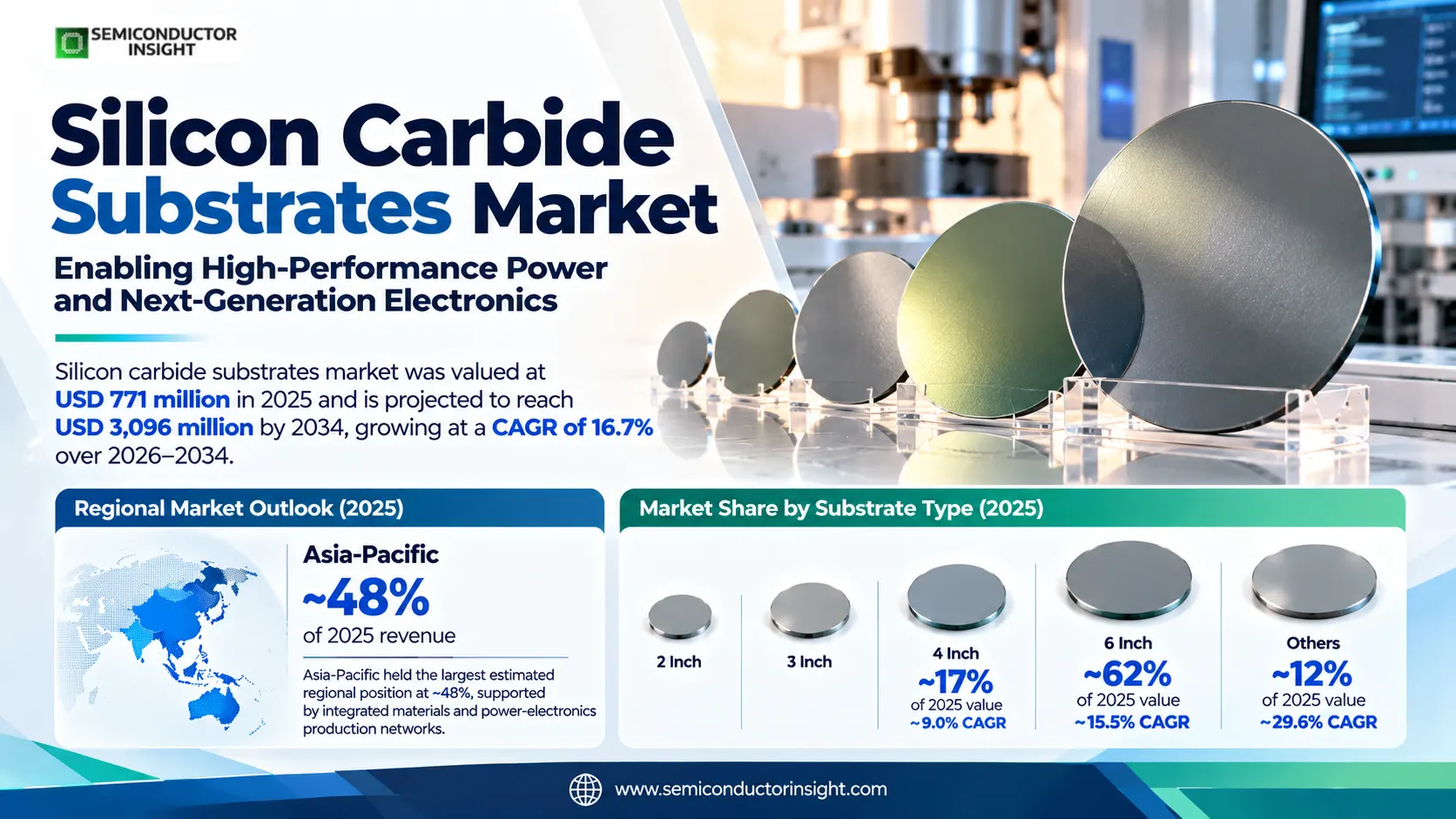
Silicon carbide substrates market was valued at USD 771 million in 2025 and is projected to reach USD 3,096 million by 2034, growing at a CAGR of 16.7% over 2026–2034. Asia-Pacific held the largest estimated regional position at ~48%, reflecting integrated materials and power-electronics production networks, sophisticated crystal-growth expertise and a growing concentration of qualified semiconductor device customers.
Silicon carbide substrates are single-crystal wafers obtained from grown SiC boules through slicing, lapping, polishing and cleaning. Their crystalline perfection determines whether downstream epitaxial layers can support high-voltage transistors, Schottky diodes or microwave transistors without unacceptable defects. Commercial orders are specified not merely by nominal diameter but by polytype, doping, orientation, resistivity, thickness uniformity, total thickness variation and surface condition. These material properties explain why supplier qualification is considerably longer than a routine purchase of industrial ceramic parts.
The revenue boundary includes finished semiconductor-grade SiC substrate wafers in the published 2 Inch, 3 Inch, 4 Inch, 6 Inch and Others diameter categories, serving power devices, electronics and optoelectronics, wireless infrastructure and other uses. The Others category accommodates sizes outside the named classes, including newer 200 mm material. Finished semiconductor devices, epitaxial processing sold as a separate service, crystal-growth equipment, complete power modules and bulk industrial SiC abrasives are outside the substrate transaction. Captively consumed wafers are relevant to supply strategy without being automatically added as independent sales.
The industrial transition is from qualified 150 mm wafers toward 200 mm formats. Coherent has explained that the larger platform offers roughly 1.8 times the usable wafer area, while Wolfspeed announced commercial availability of its 200 mm material portfolio in September 2025. A larger diameter alone does not guarantee lower cost per good die: furnace yield, boule utilization, slicing kerf, polishing damage and epitaxy defects must improve together. The buyer therefore evaluates total device cost after yield rather than substrate invoice price in isolation.
Power-conversion systems are the principal demand anchor because SiC enables efficient switching at voltages and temperatures that impose losses or thermal penalties on conventional silicon designs. Electric traction inverters, on-board chargers, solar inverters, battery storage converters and industrial motor drives pull material through device manufacturers. The International Energy Agency recorded more than 20 million electric-car sales worldwide in 2025, providing a clear downstream scale indicator. Vehicle sales are not counted as substrate revenue, but their growth helps explain the need for reliable crystal capacity.
Substrate producers operate in a market shaped by strategic offtake agreements, in-house device integration and rapidly evolving crystal technology. China is developing large-diameter n-type material; Japan contributes specialist crystal and epitaxy know-how; North American firms have invested in boule growth and material qualification; European device makers are adding local supply-chain capability. The next competitive threshold is reproducible low-defect material at 200 mm rather than a laboratory demonstration of a larger wafer. For procurement teams, multi-year contracts and dual sourcing remain important safeguards against capacity and quality shocks.
Segment Analysis: By Type
By type, substrate sales are grouped into 2 Inch, 3 Inch, 4 Inch, 6 Inch and Others. The installed 6 Inch category is largest at an estimated ~62% of 2025 value and ~15.5% modeled CAGR; 4 Inch follows at ~17% and ~9.0% growth, while Others accounts for ~12% and includes newer 200 mm material expanding at ~29.6% CAGR.
| Diameter type | Typical manufacturing role | Market position |
|---|---|---|
| 2 Inch | The 50.8 mm format serves research lots, niche compound-semiconductor lines and equipment that cannot accept larger substrates. Crystal procurement often focuses on specialized doping or experimental polytypes rather than high-volume cost reduction. Laboratories value predictable thickness, accessible wafer handling and small batch flexibility when developing new process recipes for power or optoelectronic structures. | An estimated ~4% of 2025 revenue with a modeled ~4.0% CAGR. Smaller wafers remain useful where pilot runs consume few substrates and replacing fixtures would be uneconomic. Their value is tied to custom qualification and engineering services rather than a major share of automotive production. Suppliers face limited economies of scale but can earn premiums for controlled material characteristics. |
| 3 Inch | The 76.2 mm diameter is an intermediate legacy size used in research institutes, specialty device development and older epitaxial systems. Buyers usually prioritize consistency with established lithography and handling hardware. For laboratories, a switch to 100 mm or 150 mm may require replacement of carriers, inspection equipment and process qualifications, making continued purchases rational despite inferior throughput. | The category represents ~5% of estimated 2025 value and ~6.0% modeled annual growth. Orders are comparatively fragmented and depend on the installed base of small-wafer tools. A 3 Inch substrate can be commercially attractive for unusual designs, but it does not define the cost trajectory of mainstream SiC power MOSFET manufacturing. Demand therefore remains specialized. |
| 4 Inch | The 100 mm wafer bridges older commercial power-device lines and emerging small-volume applications that require more usable die area than legacy 2 Inch or 3 Inch stock. Wafering specifications commonly emphasize edge exclusion, total thickness variation and a polishing finish compatible with epitaxial deposition. Customers may keep 100 mm tools operating for mature products with stable designs. | This type carries an estimated ~17% share in 2025 and a modeled ~9.0% CAGR. It is meaningful in established supply chains but gradually yields share to 150 mm production, where equipment utilization and die count are more favorable. Procurement can remain resilient for long-life industrial and specialty products because redesign and qualification expenses discourage abrupt wafer-size changes. |
| 6 Inch | The 150 mm platform is the current mainstream qualification base for many automotive and industrial SiC device lines. Crystal-growth recipes, slicing equipment, polishing lines and epitaxial reactors have been optimized around this diameter, supporting production-grade yield measurement and automotive traceability. Wolfspeed, Coherent and multiple device manufacturers maintain extensive experience with this generation of wafers. | With an estimated ~62% share of 2025 sales and a modeled ~15.5% CAGR, 6 Inch is the largest class. Established device designs and supplier certifications keep purchasing volumes substantial even while new facilities introduce 200 mm processes. Material quality and delivery reliability matter more than nominal diameter alone; 150 mm products retain value when process yields outperform an immature larger-wafer alternative. |
| Others | This residual category includes 8-inch and other non-enumerated sizes, most notably 200 mm SiC wafers being qualified for future power-semiconductor production. SICC publishes specifications for 200 mm 4H n-type material, while Wolfspeed offers 200 mm bare substrates and Coherent has commercial 200 mm epitaxial capabilities. Larger wafers require compatible crystal-growth and downstream handling systems. | Others represents an estimated ~12% of 2025 revenue and the highest modeled type CAGR at ~29.6%. Its rapid growth reflects transition from development and limited qualification toward commercial 200 mm supply, rather than displacement of every 150 mm line at once. Defect reduction and the usable-die economics of new production tools will determine the pace of substitution. |
Diameter transition and yield sensitivity
The nominal diameter changes the potential device count per wafer, but it also alters mechanical stresses and inspection requirements. A 200 mm wafer provides much more surface than a 150 mm wafer, yet the economic benefit depends on crystal uniformity and a low concentration of yield-limiting defects. Larger boule growth increases the importance of thermal-gradient control, stable doping and predictable off-axis orientation. These constraints create a premium for repeatable industrial material rather than headline wafer size.
Diameter-specific purchasing also changes the supplier relationship. At 2 Inch and 3 Inch, researchers may accept short runs and broader specification tolerances, while 6 Inch automotive programs demand detailed traceability and repeated lot qualification. The Others group includes newer platforms that can command development pricing before scale efficiencies appear. A 2025–2034 transition therefore involves parallel wafer generations, not a single industry-wide changeover date.
Segment Analysis: By Application
By application, the market comprises Power Device, Electronics & Optoelectronics, Wireless Infrastructure and Others. Power Device leads with an estimated ~70% share in 2025 and ~17.9% modeled CAGR; Electronics & Optoelectronics represents ~13%, Wireless Infrastructure ~12%, and remaining uses ~5%, each with distinct electrical and substrate specifications that shape purchasing contracts, crystal selection, inspection routines and qualification timelines for manufacturers.
| Application | Demand characteristics |
|---|---|
| Power Device | An estimated ~70% of 2025 substrate demand supports SiC MOSFETs, Schottky diodes and related high-voltage power components. A modeled ~17.9% CAGR reflects traction inverters, rapid charging, renewable-energy converters and industrial drives. Device makers select n-type conductive 4H-SiC for predictable resistivity, low defect density and compatibility with thick epitaxial layers. Long-term automotive contracts place exceptional weight on wafer traceability and stable qualification. |
| Electronics & Optoelectronics | This category contributes an estimated ~13% of 2025 revenue and ~13.0% modeled CAGR. It covers specialty electronic structures and optoelectronic applications where thermal conductivity, crystal stability or epitaxial compatibility makes SiC attractive. Product specifications may differ from those of traction inverter wafers, including different doping, thickness and surface conditions. The market is smaller but technically diverse, so suppliers compete on custom grades and engineering support. |
| Wireless Infrastructure | At an estimated ~12% share and ~15.0% modeled CAGR, this application includes semi-insulating substrates used beneath GaN-on-SiC radio-frequency power amplifiers. High resistivity helps isolate microwave circuits, while SiC thermal conductivity removes heat from dense base-station amplifiers. The procurement logic differs from conductive power wafers: RF customers emphasize electrical isolation, crystalline defects, thermal performance and epitaxial suitability rather than the economics of automotive MOSFET die alone. |
| Others | Remaining applications carry an estimated ~5% of 2025 revenue and ~10.0% modeled CAGR, spanning specialized sensing, scientific instrumentation and industrial electronics not classified elsewhere. Development programs may require uncommon orientations, small volumes or higher-price mechanical grades for qualification experiments. Commercialization depends on whether a device architecture moves from laboratory trials to repeat orders; this category therefore has a wider spread of technical requirements than mainstream power conversion. |
The application split changes wafer acceptance testing. Automotive power-device makers focus on leakage and long-life reliability under high temperature, while RF amplifier manufacturers prioritize semi-insulating resistivity and thermal dissipation. Electronics and optoelectronics projects may require unusual epitaxial stacks or special surface preparation. Although the same crystal-growth supplier can serve multiple applications, switching a qualified wafer grade is not a simple purchasing substitution, because downstream defect sensitivity and electrical performance differ significantly.
Regional Analysis
Asia-Pacific is the largest silicon carbide substrate market at an estimated ~48% of 2025 revenue, followed by North America at ~24% and Europe at ~19%. South America contributes ~4% and the Middle East & Africa ~5%. Asia-Pacific has a modeled ~18.1% CAGR because crystal producers, device fabs and electric-vehicle supply chains cluster across China, Japan, South Korea and Southeast Asia.
Why are SiC substrate supply and demand distributed unevenly across regions?
Regional purchasing reflects where wafers are grown, where power devices are fabricated and where the resulting inverters or RF components are integrated into end products. A supplier may manufacture crystal boules in one country, slice and polish substrates in another and ship finished wafers to a separate device fab. This geographic division means automotive sales alone do not reveal substrate revenue location; long-term qualification contracts and semiconductor manufacturing footprints matter more directly.
Asia-Pacific combines the broadest range of upstream and downstream activities, while North America has historically contributed important crystal-growth expertise and proprietary material processes. Europe is expanding vertical integration in Italy, with a manufacturing focus on power semiconductors and SiC substrates. South America and the Middle East & Africa remain smaller direct substrate markets because most downstream systems are imported, although industrial electrification creates demand for the power components fabricated from SiC elsewhere.
| Region | Position | Growth outlook | Demand profile | What decides supplier selection |
|---|---|---|---|---|
| Asia-Pacific | Largest (~48%) | Fastest (~18.1% CAGR) | Integrated materials and device fabs | Large-diameter qualification, local customer proximity and production yield |
| North America | Second (~24%) | Mature technology (~15.0% CAGR) | Crystal growth and materials supply | Automotive qualification, contract visibility and cost per usable wafer |
| Europe | Third (~19%) | Capacity-building (~15.2% CAGR) | Vertical integration and industrial power | Supply security, industrial reliability and equipment conversion |
| South America | Emerging (~4%) | Selective (~15.5% CAGR) | Imported power-electronics ecosystems | Application engineering, distribution channels and import costs |
| Middle East & Africa | Smaller (~5%) | Project-driven (~16.5% CAGR) | Energy and infrastructure demand | Grid project schedules, technical support and thermal robustness |
Leading Silicon Carbide Substrate Suppliers and Competitive Landscape
The competitive landscape combines independent wafer vendors, materials specialists and vertically integrated semiconductor manufacturers. Crystal quality, diameter capability and customer qualification determine market access more directly than corporate sales size. Wolfspeed, Coherent and SICC have published large-diameter material offerings, while European and Japanese groups are developing substrate integration and advanced epitaxy technologies for demanding industrial customers.
Substrate competition is not equivalent to competition in finished SiC MOSFETs. A device producer may grow its own crystals, purchase bare wafers from an external specialist or buy epitaxial wafers from a materials partner. These arrangements carry different revenue recognition and qualification obligations. Coherent sells conductive and semi-insulating materials, Wolfspeed has commercialized 200 mm wafers, and SICC documents n-type products with detailed geometry and crystal specifications. Comparing total company revenue would distort their positions in this particular material category.
Former corporate names require care when assessing supplier rosters. Cree materials operations are now associated with Wolfspeed; II-VI Advanced Materials belongs under Coherent; Norstel became part of STMicroelectronics after its 2019 acquisition; and Showa Denko businesses operate within Resonac. SiCrystal is part of the ROHM group. Historical names remain relevant to long-running qualifications, but counting a parent and its acquired brand as separate independent market leaders would exaggerate competition and could confuse procurement teams.
Product leadership can differ between n-type conductive wafers for power conversion and semi-insulating wafers for radio-frequency amplifiers. The latter require extremely high electrical resistance while retaining the thermal advantages of SiC, whereas power devices generally use controlled conductive doping. Material suppliers therefore specialize in distinct crystal and finishing recipes. A company with a strong RF qualification history is not automatically the best source for 200 mm automotive substrates, and the reverse is also true.
The central commercial barrier is reproducibility. Customers request defect maps, surface roughness data, thickness measurements, electrical characteristics and multi-lot evidence before allowing a new wafer grade into a production device flow. Large investments in growth furnaces can fail to produce proportionate revenue if usable crystal yield is poor. Suppliers that combine reliable process control with sufficient wafer volume, technical support and secure logistics are better positioned to capture long-duration supply agreements than entrants selling only pilot samples.
Tier structure
| Tier | Companies | Basis of competition |
|---|---|---|
| Tier 1 | Wolfspeed; Coherent; SICC | Established commercial substrate product families, demonstrated large-diameter capabilities and direct customer qualification programs. |
| Tier 2 | STMicroelectronics / Norstel; ROHM / SiCrystal; Resonac; TankeBlue | Integrated or specialist materials capabilities with differentiated crystal, epitaxial or process technologies. |
| Specialist / historical | DuPont / Dow Corning; Nippon Steel & Sumitomo Metal; Hebei Synlight Crystal; CETC | Names appearing in historical or specialist market rosters; current independent merchant substrate activity requires product-specific verification. |
Key companies profiled
- Wolfspeed (formerly Cree)
- Coherent (formerly II-VI Advanced Materials)
- SICC
- ROHM / SiCrystal
- STMicroelectronics / Norstel
- Resonac (formerly Showa Denko)
- TankeBlue
- DuPont / Dow Corning (historical listing)
- Nippon Steel & Sumitomo Metal (historical listing)
- Hebei Synlight Crystal
- CETC
Silicon Carbide Substrate Manufacturing and Capacity Outlook
Production economics begin with high-temperature crystal growth and extend through boule inspection, slicing, lapping, polishing and wafer metrology. The transition from 150 mm to 200 mm increases potential output per wafer but requires new control of thermal gradients and defect formation. Capacity announcements must therefore be evaluated against usable-wafer yield and the time required for downstream customer certification.
The upstream process creates a single-crystal boule using controlled silicon and carbon sources under demanding thermal conditions. Producers then orient, cut and polish wafers to strict flatness and roughness specifications. Micropipes, basal-plane dislocations, stacking faults and other crystal defects can degrade device performance after epitaxy, so inspection is an integral cost center. Even when two suppliers quote the same nominal 150 mm diameter, different defect distributions can lead to materially different device yields and qualification outcomes.
Wafer diameter is a productivity lever rather than an automatic cost-saving guarantee. Coherent began 200 mm epitaxial wafer shipments in 2024, and its technology disclosures emphasize low defect density and uniform thickness and doping. Wolfspeed moved a commercial 200 mm materials portfolio into broader customer availability in 2025. Device makers may operate 150 mm and 200 mm lines concurrently because redesigning a qualified process requires equipment conversion, reliability tests and customer acceptance that extend beyond crystal growth alone.
Investment in device fabrication creates a pull for substrates but cannot be converted directly into wafer-market sales. SEMI projected record 200 mm fab capacity above 7.7 million wafers per month by 2026 across many semiconductor technologies, not solely SiC. Infineon and STMicroelectronics have announced major wide-bandgap production programs, illustrating downstream capital intensity. A robust substrate forecast separates these adjacent investments from the actual value of bare single-crystal material shipped to device producers.
Silicon Carbide Substrate Market Dynamics and Growth Opportunities
Demand expansion is driven by electrification and high-efficiency power conversion, while the largest constraints are wafer manufacturing cost, crystalline defects and the length of customer qualification. Larger-diameter commercialization adds an important second growth vector. The impact assessment assigns positive and negative percentage-point contributions to the modeled 2026–2034 CAGR and distinguishes early production ramp effects from longer-term technology adoption.
MARKET DRIVERS
Drivers Impact Analysis*
| Market Drivers | Impact Rank | CAGR Contribution (%) | 2026–2028 | 2029–2031 | 2032–2034 |
|---|---|---|---|---|---|
| Electric-vehicle traction inverter and charging demand | High | +6.80% | High | High | Medium |
| 200 mm wafer scale-up and new customer qualifications | Medium-High | +5.10% | Medium | High | High |
| Renewable-energy and grid power conversion | Medium | +3.40% | Medium | High | High |
| Industrial automation and higher-efficiency drives | Low-Medium | +2.70% | Medium | Medium | High |
| Others (RF infrastructure, data-center power and specialty devices) | Low | +1.60% | Low | Medium | Medium |
Vehicle electrification expands the high-voltage device pipeline
Electric cars require efficient traction conversion, on-board charging and power management, creating sustained demand for qualified conductive SiC material. The International Energy Agency recorded more than 20 million electric-car sales in 2025 and expected further adoption in 2026, although the regional pace differs. Substrate suppliers benefit when device manufacturers commit to repeat wafer purchases after design qualification; the vehicle count itself is only an indicator of the downstream opportunity.
Larger wafers change the unit-cost equation
Commercial 200 mm supply is widening the set of manufacturing options available to power-device producers. Compared with 150 mm stock, the larger diameter can increase potential die output per processing step and improve equipment productivity. However, a material transition requires stable defect maps and a consistent supply of usable crystal. Vendors that prove reliable quality over repeated lots may capture additional customers without competing solely through lower nominal wafer prices.
Renewable generation and storage need efficient power stages
Solar inverters, battery energy storage systems and grid interfaces use power devices to convert electricity between direct and alternating current. Silicon carbide can lower switching losses and support compact thermal designs, especially where voltage and efficiency requirements are demanding. The Department of Energy has demonstrated the role of SiC in photovoltaic conversion research. Material demand rises when such devices move from engineering prototypes to standardized commercial converter platforms.
Industrial electrification broadens the customer base
Motor drives, factory automation, rail traction and high-power electrical systems provide a demand stream distinct from passenger vehicles. Equipment makers assess energy savings over long duty cycles, maintenance intervals and cooling requirements when choosing SiC power semiconductors. Substrate suppliers must offer grades that can withstand device qualification across diverse industrial voltage classes. This diversification can moderate dependence on a single automotive production cycle.
MARKET RESTRAINTS
Restraints Impact Analysis*
| Market Restraints | Impact Rank | CAGR Contribution (%) | 2026–2028 | 2029–2031 | 2032–2034 |
|---|---|---|---|---|---|
| Crystal defects, polishing losses and usable-wafer cost | High | -1.40% | High | High | Medium |
| Long device qualification and diameter conversion cycles | Medium | -0.90% | High | Medium | Medium |
| Others (price competition, financing and alternative materials) | Low | -0.60% | Medium | Medium | Low |
Crystal quality remains the decisive manufacturing bottleneck
SiC boules are difficult to grow at large diameters with uniform electrical and structural characteristics. Defect-sensitive power devices can lose substantial yield when wafer flaws propagate into epitaxial layers, making the cost per acceptable substrate more relevant than furnace nameplate output. New 200 mm programs can initially face higher inspection and processing expenses. Price pressure therefore may arrive before producers have fully realized the expected scale benefits.
Qualification cycles delay conversion of announced capacity into sales
An automotive device manufacturer does not substitute a new substrate after a single laboratory test. Qualification involves repeated epitaxial runs, device fabrication, accelerated reliability studies and evidence that wafer characteristics remain consistent across shipments. These steps can consume many quarters and require technical teams from both supplier and customer. Capital investment may precede revenue recognition by a long interval, especially during a transition between wafer diameters.
Alternative technologies and customer capital budgets affect timing
Conventional silicon remains cost-effective in many lower-voltage power applications, while gallium nitride competes in selected high-frequency conversion and RF architectures. Device manufacturers also adjust fab expansion schedules when electric-vehicle orders or industrial investment weaken. A substrate supplier may consequently face order volatility even when the long-term technology case is intact. Flexible production planning and customer diversification are important responses to this cyclical risk.
MARKET OPPORTUNITIES
200 mm automotive substrate qualification
A materials supplier that demonstrates consistent 200 mm defect control can address a growing pool of power-device manufacturers investing in larger wafer lines. Wolfspeed, Coherent and SICC provide visible examples of the technology transition. Commercial differentiation will rest on usable wafer yield, epitaxial performance and reliable delivery rather than diameter alone. The opportunity is strongest where suppliers support joint process development and provide detailed quality traceability.
Bonded substrates and alternative crystal utilization
Resonac and Soitec are jointly exploring 200 mm bonded SiC structures as a route to more efficient use of premium crystal material. If device makers validate the electrical and mechanical performance, such approaches could reduce the amount of bulk single-crystal material required per processed wafer. That would change supplier economics and potentially create new product categories. Adoption depends on qualification and manufacturing cost, not just successful research demonstrations.
High-voltage industrial and data-center conversion
Coherent disclosed thick SiC epitaxy capabilities for power devices up to 10 kV in April 2026, linking material technology with demanding industrial and data-center power applications. Higher voltage architectures can require different epitaxial thickness and defect specifications from mainstream automotive designs. Substrate producers that work closely with epitaxy specialists can capture high-value qualification opportunities even if these applications remain smaller in unit volume than vehicle power electronics.
RF substrates and advanced wireless amplifiers
Semi-insulating SiC remains valuable beneath gallium nitride RF structures because it combines high electrical isolation with effective heat spreading. Coherent markets dedicated semi-insulating material for RF amplifiers, demonstrating a technically distinct market from conductive power wafers. Substrate suppliers can pursue premium specialty grades by controlling resistivity and surface quality, although demand is linked to base-station capital expenditure and the timing of next-generation wireless deployments.
Silicon Carbide Substrate Value Chain and Procurement
The supply chain links raw materials and high-temperature crystal growth to boule slicing, wafer finishing, epitaxial deposition, power-device fabrication and end-equipment assembly. A substrate may cross several corporate or national boundaries before reaching a traction inverter or radio amplifier. Technical qualification and material traceability are therefore central to commercial resilience, particularly as 200 mm wafer platforms enter broader production.
Upstream material preparation. Crystal-growth teams control high-temperature processing, seed selection and doping to produce boules with stable electrical and structural characteristics. These operations demand specialized equipment, experienced engineers and extensive metrology. The quality of the grown crystal constrains the economics of every later step, because slicing cannot remove bulk defects already present in the material. Customers increasingly request traceable defect metrics rather than relying on nominal diameter or generic semiconductor-grade labels.
Wafer fabrication and finishing. Boules are sliced into wafers, flattened, polished and cleaned before inspection and packing. Material lost in the saw kerf and during surface correction reduces the number of saleable substrates, while insufficient polishing can cause epitaxial defects. The move to 200 mm changes handling forces and equipment compatibility, requiring investment in inspection and processing tools. Manufacturers that improve throughput without sacrificing surface quality can defend margins during price competition.
Distribution and qualification. Most high-volume substrates are supplied directly under negotiated agreements to device or epitaxial wafer manufacturers rather than through commodity distribution. The buyer evaluates wafer bow, thickness variation, electrical resistivity, crystalline defects and lot traceability against the intended fabrication flow. Qualification costs create durable relationships but also raise the penalty for delayed shipments or inconsistent material. Multi-year contracts can improve capacity planning for both crystal growers and power-semiconductor producers.
Downstream conversion. Epitaxial layers and device fabrication convert substrate properties into functional power or RF components, which are then packaged for automotive, industrial, energy and communication equipment. The final system value is much greater than the bare-wafer sale and must not be used as a substitute for material-market revenue. Feedback from device yield and field reliability informs future crystal specifications, so the supply chain operates as a technical partnership rather than a simple sequence of spot transactions.
Recent Developments in Silicon Carbide Substrate Technology
- 15 October 2026 Agreement
Wolfspeed and Infineon expanded a long-running silicon carbide wafer supply arrangement to include 200 mm substrates alongside 150 mm products. The extension illustrates the growing commercial importance of qualified larger-diameter supply rather than isolated pilot wafers. For materials manufacturers, the agreement connects customer visibility with the capital and process development needed for sustained crystal output. Source - 9 April 2026 Technology
Coherent reported production-capable 150 mm and 200 mm thick SiC epitaxy platforms supporting high-voltage devices up to 10 kV. The development is relevant to advanced industrial power and data-center conversion, where thicker epitaxial layers impose demanding defect and uniformity requirements. It broadens the technical range of applications served by qualified substrate and epitaxy combinations. Source - 3 December 2025 Milestone
Coherent announced progress on a 300 mm silicon carbide materials platform aimed primarily at thermal management in artificial-intelligence data centers. The platform sits beyond the diameter classes named individually in this study and illustrates a longer-term direction for material engineering. Its significance is technological optionality; the announcement does not establish current mass-market substrate revenue at that diameter. Source - 10 September 2025 Commercial
Wolfspeed launched commercial availability of its 200 mm SiC materials portfolio after earlier supply to selected customers, with associated epitaxy offered for immediate qualification. The launch gives device manufacturers a clearer sourcing route for larger-diameter wafers. Commercial release remains distinct from full qualification at every customer fab, so adoption can progress at different speeds. Source - 16 July 2025 Recognition
Resonac received a Japanese green-chemistry award recognizing its high-quality SiC epitaxial wafer technology for power semiconductors. The award points to the role of epitaxial quality in the wider materials ecosystem, where defects inherited from substrates influence downstream device performance. Recognition of technical achievement does not itself imply a quantified market-share change or additional wafer shipments. Source - 2025 Manufacturing
STMicroelectronics outlined changes to its production network that preserve Catania as a power and wide-bandgap semiconductor center, with emphasis on a 200 mm SiC campus. The program links manufacturing scale to local materials competence and specialized engineering. It also underscores that capital spending on device fabs should be distinguished from sales of finished bare SiC substrates. Source - 26 September 2024 Launch
Coherent announced shipments of 200 mm n-type SiC epitaxial wafers, describing 350 micrometre and 500 micrometre substrate thickness options and improved usable area relative to 150 mm. The launch provides a concrete indicator of the commercial wafer-size transition. For customers, thickness and doping consistency remain critical because material imperfections can reduce device yield after epitaxy. Source - 24 September 2024 Partnership
Resonac and Soitec agreed to jointly develop 200 mm bonded silicon carbide substrates for power semiconductor epitaxial wafers. The collaboration seeks to improve material utilization and broaden the supply chain through bonding technology. Industrial adoption depends on customer validation of mechanical integrity, electrical performance and processing compatibility, so the partnership is a development milestone rather than proof of completed commercialization. Source - 8 August 2024 Facility
Infineon inaugurated the first phase of its 200 mm SiC power-semiconductor fab in Kulim, Malaysia, supporting its wider electrification strategy. The investment is a downstream device-manufacturing milestone that can increase the need for qualified substrate inputs. It is not treated as direct substrate revenue, because fab capacity covers multiple processing steps and depends on actual utilization. Source
REPORT SCOPE & SEGMENTATION
| Attribute | Details |
|---|---|
| Study Period | 2020–2034 |
| Base Year | 2025 |
| Estimated Year | 2026 |
| Forecast Period | 2026–2034 |
| Historical Period | 2020–2024 |
| Market Size 2025 | USD 771 million |
| Market Size 2026 | USD 900 million |
| Market Size 2034 | USD 3,096 million |
| Growth Rate | CAGR of 16.7% during 2026–2034 |
| Unit | Revenue (USD Million); wafer diameters in inches or millimetres |
| Segmentation | By Type, By Application, and By Region |
| By Type | 2 Inch · 3 Inch · 4 Inch · 6 Inch · Others (including 8-inch and emerging sizes) |
| By Application | Power Device · Electronics & Optoelectronics · Wireless Infrastructure · Others |
| By Region | Five geographic blocks analyzed by application, country and supply-chain role North AmericaUnited States, Canada, Mexico EuropeItaly, Germany, France, United Kingdom, Rest of Europe Asia-PacificChina, Japan, South Korea, Taiwan, Malaysia, Rest of Asia-Pacific South AmericaBrazil, Argentina, Chile, Rest of South America Middle East & AfricaSaudi Arabia, UAE, South Africa, North Africa, Rest of region |
| Key Companies Profiled | Wolfspeed; Coherent; SICC; ROHM / SiCrystal; STMicroelectronics / Norstel; Resonac; TankeBlue; DuPont / Dow Corning; Nippon Steel & Sumitomo Metal; Hebei Synlight Crystal; CETC |
| Customization Scope | Country and end-use breakouts, diameter-specific material qualification, conductive versus semi-insulating grades, 200 mm transition scenarios and supplier-level manufacturing intelligence can be added through project customization. |
Frequently Asked Questions
What is the current size and growth outlook for the silicon carbide substrates market?
The global silicon carbide substrates market was valued at USD 771 million in 2025 and is projected to reach USD 3,096 million by 2034, representing 16.7% CAGR during 2026–2034. The 2026 estimate is USD 900 million. Expansion is associated with high-efficiency power electronics, new wafer diameters and demand for more reliable crystalline material in automotive and industrial device fabrication.
What exactly is included in silicon carbide substrate revenue?
The category measures finished semiconductor-grade single-crystal SiC wafers sold or valued as substrate products. It covers the published diameter and application groups, including conductive wafers for power devices and semi-insulating grades for RF electronics. It excludes the selling value of complete power modules, finished transistors, fabrication machinery and unrelated industrial SiC products. Epitaxial services are distinguished from the bare substrate transaction.
Which substrate diameter is the largest commercial category?
The 6 Inch class leads with an estimated ~62% of 2025 revenue because 150 mm technology has an established production and qualification base. The 4 Inch class accounts for ~17%, while Others contributes ~12% and includes newer 200 mm formats. Smaller 2 Inch and 3 Inch substrates remain useful in specialist processes, but their contribution is much lower than the mainstream power-device wafer size.
Which end-use application accounts for the most SiC wafers?
Power Device is the largest application at an estimated ~70% of 2025 substrate value, reflecting the material requirements of MOSFETs, diodes and high-efficiency converters. Electronics & Optoelectronics accounts for ~13%, and Wireless Infrastructure for ~12%. RF uses often require semi-insulating crystal grades, while traction and industrial power systems generally use conductive material. Customer specifications therefore differ significantly across end uses.
Which region leads global silicon carbide substrate activity?
Asia-Pacific leads with an estimated ~48% share of 2025 revenue and a modeled ~18.1% CAGR. China, Japan and nearby manufacturing hubs combine crystal suppliers, epitaxial expertise and device fabs with substantial electronics and vehicle production. North America contributes ~24% and Europe ~19%, reflecting important materials technology and industrial semiconductor capabilities. Geographic shares are modeled estimates rather than independently audited transaction totals.
Why is the transition to 200 mm silicon carbide important?
Larger 200 mm wafers offer more usable surface area per processing cycle than 150 mm material and can improve semiconductor manufacturing productivity when quality is maintained. The benefit depends on crystal defects, polishing yield and compatibility with epitaxial and device equipment. Suppliers have begun commercial 200 mm offerings, but device makers still need multi-lot qualifications. The transition therefore takes place over several production generations rather than overnight.
How do substrate manufacturers compete beyond price?
Suppliers differentiate through low micropipe and dislocation density, thickness uniformity, reliable resistivity, surface finish and repeatable lot performance. Automotive and industrial customers value traceability and consistent epitaxial outcomes because substrate defects can propagate into costly device failures. Secure capacity, technical cooperation and long-term delivery agreements further affect supplier selection. A low quoted wafer price can be unattractive if usable device yield is inferior.
What are the biggest risks to the market forecast?
Crystal-growth yield, long automotive qualification cycles and slower-than-planned device-fab ramps can postpone substrate revenue. The industry also faces pressure from alternative semiconductor technologies in some voltage ranges and from customers adjusting capital expenditure. A larger nominal wafer diameter is not proof of commercial cost advantage until defects and downstream processing losses are controlled. These risks can produce uneven annual growth even when the longer-term application opportunity remains strong.
Which companies are active in silicon carbide substrate supply?
Notable current material providers include Wolfspeed, Coherent and SICC, alongside integrated or specialist capabilities associated with STMicroelectronics, ROHM / SiCrystal and Resonac. Historical lists may contain Cree, II-VI, Norstel and Showa Denko, which now correspond to successor organizations. Suppliers serve different conductive, semi-insulating and epitaxial material needs, so a single undifferentiated ranking does not capture all relevant technical markets.
What period and segmentation does the study cover?
The analysis uses 2025 as the base year, 2026 as the estimated year and 2034 as the forecast endpoint, with historical context from 2020 through 2024. Type coverage consists of 2 Inch, 3 Inch, 4 Inch, 6 Inch and Others; applications include Power Device, Electronics & Optoelectronics, Wireless Infrastructure and Others. Five regional blocks provide geographic coverage, with modeled market positions and growth rates.
Research Sources & Evidence Base
Get Sample Report PDF for Exclusive Insights
Report Sample Includes
- Table of Contents
- List of Tables & Figures
- Charts, Research Methodology, and more...
 Download Sample Report PDF