Key Statistics
Key Takeaways
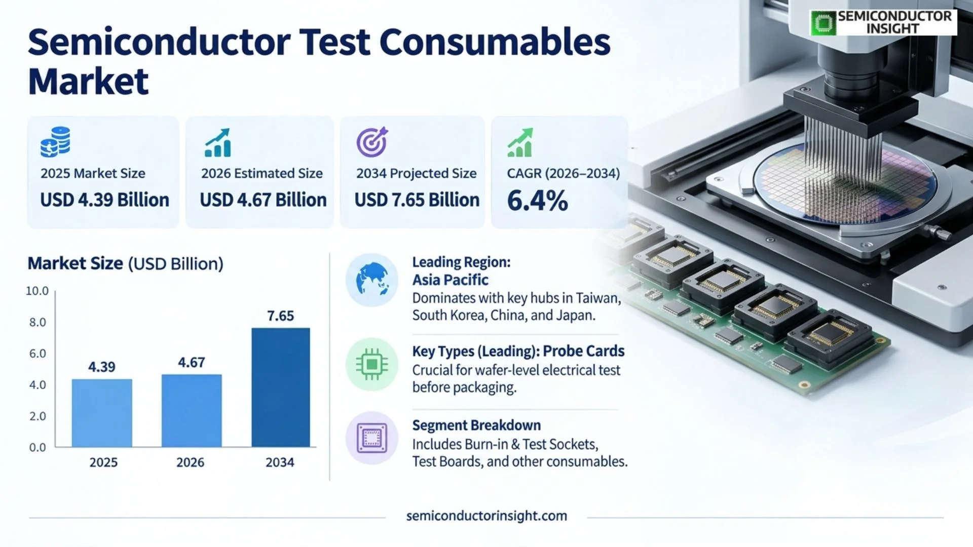
- Market size and growth: the market is estimated at USD 4.67 billion in 2026 and is projected to reach USD 7.65 billion by 2034, representing a 6.4% CAGR during 2026–2034.
- Probe cards remain the largest product category because every wafer must be electrically contacted before dicing, while advanced logic, HBM and fine-pitch devices require increasingly complex interfaces.
- AI and HBM are raising test intensity through higher pin counts, greater current density and more parallel test channels, increasing the value of qualified contact technology per device.
- Asia Pacific leads because foundries, memory manufacturers and OSATs are concentrated in Taiwan, South Korea, China and Japan, creating the deepest installed base for recurring probe-card and socket replacement.
- Supplier capacity is expanding for advanced test: FormFactor reported USD 637.9 million of Probe Cards revenue in fiscal 2025 and disclosed a new Texas manufacturing site expected to begin ramping in late fiscal 2026.
Semiconductor Test Consumables Market Overview
Semiconductor Test Consumables Market was valued at USD 4.39 billion in 2025 and is estimated at USD 4.67 billion in 2026. The market is projected to reach USD 7.65 billion by 2034, representing a CAGR of 6.4% during 2026–2034. Asia Pacific is the largest regional market because Taiwan, South Korea, China and Japan combine the world’s largest concentration of semiconductor fabrication, memory production and outsourced assembly-and-test capacity.
Base year: 2025 · Estimated year: 2026 · Forecast period: 2026–2034 · Values in USD million unless otherwise stated
Semiconductor test consumables are the physical interfaces used to connect wafers or packaged devices to automated test equipment. The category includes probe cards for wafer sort, burn-in and final-test sockets, test boards, contactors and related high-wear components. These products are essential because every semiconductor must be screened for functionality, timing, power, signal integrity and reliability before shipment. Consumables scale with device volume, but their value per test increases when pad pitch, pin count, signal frequency, current density and thermal load become more demanding.
Probe cards provide temporary electrical contact to die pads or bumps before dicing, while sockets and contactors support packaged-device burn-in and final test. Both categories operate under repeated mechanical cycling and therefore have finite service lives. Advanced AI processors, HBM stacks, high-current power devices and RF components place very different demands on contact geometry and materials, which prevents one universal interface from serving the entire market. Suppliers compete through contact resistance, planarity, lifetime, signal integrity, cleaning frequency and application-specific engineering.
FormFactor reported USD 637.9 million of Probe Cards revenue in fiscal 2025 and linked demand to generative-AI infrastructure, including HBM and co-packaged optics. This demonstrates that test consumables grow not only with semiconductor unit volume but also with device complexity. More contacts, higher parallelism and tighter pitch can raise the value of the interface used at each test insertion, while recurring wear creates replacement demand throughout the life of a semiconductor production program.
Segment Analysis: By Type
By type, the market is segmented into probe cards, aging and test sockets, test boards and other consumables. Probe cards lead because wafer-level electrical test occurs before packaging and requires precise repeated contact to increasingly dense pad arrays. Burn-in and final-test sockets remain critical for packaged devices, while test boards route signals between automated test equipment and the device interface. Product value rises materially with frequency, current, pin count and mechanical complexity.
| Type | Technical / commercial role | Market position |
|---|---|---|
| Probe Cards | MEMS, vertical and cantilever interfaces used for wafer-level electrical test. | Largest segment; advanced logic, HBM and fine-pitch devices drive higher contact density and value. |
| Aging & Test Sockets | Burn-in and final-test interfaces for packaged semiconductors. | Recurring demand tied to insertion cycles, temperature exposure and package transitions. |
| Test Boards | Interface boards connecting tester channels to probe cards or sockets. | High-value custom designs matched to specific testers, packages and signal requirements. |
| Others | Contactors, interposers, probe needles and specialized test interfaces. | Niche but technically critical across RF, power, MEMS and engineering test. |
Segment Analysis: By Application
Applications include consumer electronics, medical devices, automotive and other semiconductor end markets. Consumer electronics generates large chip volumes, while automotive and medical devices often require more intensive reliability testing. AI accelerators, networking silicon and HBM increase the value per interface because they require very high pin counts, high-speed signals and large parallel test configurations. Automotive power and analog devices add high-current and high-temperature requirements that accelerate wear and support specialized consumable designs.
| Application | Demand characteristics |
|---|---|
| Consumer Electronics | High semiconductor volumes across smartphones, PCs, wearables and appliances support broad wafer-sort and final-test demand. |
| Medical Devices | Reliability and traceability requirements support high-quality interfaces for regulated electronics and sensing devices. |
| Automotive | Power, analog, MCU and ADAS devices require stringent temperature, current and lifetime validation. |
| Others | Includes AI/HPC, networking, industrial, RF and memory devices with increasingly specialized test needs. |
Segment Analysis: By Device Test Stage
Test stage is commercially important because wafer sort, burn-in and final test use different interfaces and replacement cycles. Wafer sort relies on probe cards before dicing, burn-in stresses devices for extended periods at elevated temperature, and final test verifies packaged parts at production speed. Engineering characterization uses lower-volume but highly flexible interfaces. Suppliers that serve multiple stages can capture a larger share of customer spending and support device programs as they transition from development into high-volume manufacturing.
| Test Stage | Consumable demand |
|---|---|
| Wafer Sort | Probe cards, probes and interface boards for pre-package screening. |
| Burn-in | Sockets and boards designed for long dwell times and elevated temperature. |
| Final Test | High-cycle sockets, contactors and interface boards for packaged devices. |
| Characterization & Engineering | Flexible probe and socket solutions used during device development and qualification. |
Segment Analysis: By Semiconductor Device Class
Device class changes the electrical and mechanical burden placed on test consumables. Logic and AI devices require high pin counts, fine pitch and strong signal integrity; memory and HBM emphasize parallelism and dense arrays; power devices require high current and thermal control; RF devices need low-loss high-frequency interfaces. This segmentation explains why suppliers maintain multiple probe and socket technologies rather than attempting to use one contact architecture across all semiconductor customers.
| Device Class | Key test requirement |
|---|---|
| Logic & AI | Fine pitch, high pin count, high-speed signal integrity and large parallelism. |
| Memory & HBM | Dense arrays, parallel testing and stable contact across many channels. |
| Power Semiconductors | High current, temperature control and durable contact surfaces. |
| RF & Analog | Low-loss high-frequency interfaces and precise analog signal integrity. |
Regional Analysis
Asia Pacific is the largest regional market because semiconductor fabrication, memory production and outsourced assembly-and-test operations are concentrated in Taiwan, South Korea, China and Japan. North America retains strong demand in advanced logic, AI and test technology, while Europe is important for automotive, industrial and power-semiconductor applications. Regional supply chains are tightly connected because many U.S. and European test-interface suppliers manufacture or support customers in Asia.
Test consumables follow semiconductor manufacturing more closely than final device consumption. A chip designed in the United States can be fabricated and tested in Taiwan, South Korea or Southeast Asia, meaning the consumable sale occurs near the fab or OSAT rather than where the final server or smartphone is sold. This makes Asia Pacific structurally dominant, while North America and Europe retain high-value design, engineering and specialized-device demand that supports advanced contact technologies.
| Region | Position | Growth outlook | Demand profile | Supplier-selection factor |
|---|---|---|---|---|
| Asia Pacific | Largest | High | Foundries, memory and OSATs | Fine pitch, capacity and local service |
| North America | High-value | High | AI, logic and test technology | Advanced performance and engineering |
| Europe | Established | Moderate-High | Automotive, industrial and power | Reliability and high-current capability |
| South America | Small | Selective | Limited front-end manufacturing | Import support and cost |
| Middle East & Africa | Emerging | Selective | Israel and technology projects | Qualification and global supply |
Competitive Landscape
Competition is led by specialist probe-card and socket manufacturers whose intellectual property lies in contact technology, MEMS fabrication, mechanical design and signal integrity. FormFactor, Technoprobe, Japan Electronic Materials, Micronics Japan, MPI and other suppliers compete for advanced wafer-test positions, while socket and board specialists address packaged-device test. Qualification cycles are long because a contact interface directly affects yield, throughput and test accuracy, creating durable positions for suppliers that prove consistent field performance.
FormFactor reported USD 637.9 million of Probe Cards revenue in fiscal 2025 and stated that HBM and other AI-related infrastructure demand supported growth. The company also disclosed a Texas manufacturing site expected to begin ramping production in late fiscal 2026. These investments illustrate how leading suppliers are adding qualified capacity for more complex compute and memory products rather than treating probe cards as a mature, low-growth category.
Technoprobe, Micronics Japan and Japan Electronic Materials compete strongly in high-density wafer probing, while MPI, SV Probe and Korea Instrument bring regional specialization. Fine-pitch MEMS technologies require substantial process expertise and capital. Customers evaluate contact resistance, probe life, planarity, cleaning frequency and throughput, so a relatively small performance advantage can create significant economic value when a high-volume production tester operates continuously.
Packaged-device testing adds another competitive layer through burn-in and final-test sockets, contactors and boards. These products must evolve as chiplets, high-current power devices and high-speed interfaces become more common. Suppliers with strong mechanical simulation, advanced materials and rapid engineering cycles can win designs before production ramps, creating a recurring replacement stream once the package enters volume manufacturing.
| Competitive tier | Representative companies | Competitive basis |
|---|---|---|
| Global probe-card leaders | FormFactor, Technoprobe, Japan Electronic Materials, Micronics Japan | Advanced MEMS or vertical probing, large customer bases and high-end logic/memory capability. |
| Regional / specialized probe suppliers | MPI, SV Probe, Korea Instrument, Wentworth Laboratories | Local service, memory/RF specialization and flexible engineering. |
| Test-interface specialists | Feinmetall, FICT, TOHO Electronics, GGB Industries | Sockets, boards, contactors and specialized engineering interfaces. |
Key Participants
The profiled competitive set includes FormFactor, Inc., Japan Electronic Materials (JEM), Wentworth Laboratories, Technoprobe S.p.A., Micronics Japan Co., Ltd., MPI Corporation, SV Probe Co., Ltd., Korea Instrument Co., Ltd., FICT LIMITED, Feinmetall GmbH, TOHO ELECTRONICS INC., GGB Industries (PICOPROBE). Supplier position depends on engineering performance, customer qualification, manufacturing continuity and the ability to support design changes over long product cycles. Larger vendors benefit from broad portfolios and application teams, while specialists can retain strong positions in narrow, technically demanding subsegments where historical qualification and process know-how create meaningful switching costs.
Production Capacity Analysis
Probe-card capacity depends on MEMS fabrication, ceramic or organic substrates, probe assembly, planarity control and final electrical characterization. High-end products can contain thousands of contacts and require tight mechanical tolerances, so effective capacity is constrained by yield and engineering complexity rather than simple unit count. As HBM and AI devices increase pin counts, the manufacturing burden per probe card rises and qualified capacity becomes more valuable.
FormFactor disclosed that it purchased a Texas manufacturing site expected to begin ramping production in late fiscal 2026. Expansion of qualified manufacturing close to major U.S. semiconductor customers can reduce lead times and support geographic diversification, but a new factory must reproduce established contact performance before customers accept it for production test. Qualification therefore determines how quickly physical floor space can become commercially usable output.
Upstream materials include tungsten and specialty probe alloys, ceramics, high-frequency laminates, springs and precision-machined hardware. Package and wafer-test requirements are moving simultaneously toward finer pitch and higher current, creating conflicting material needs. Suppliers that vertically control critical probe or MEMS technologies can improve consistency, preserve intellectual property and reduce exposure to shortages in specialized upstream components.
| Capacity factor | Market implication |
|---|---|
| MEMS / probe fabrication | Determines fine-pitch contact density and high-end probe-card output. |
| Substrates and interface boards | Control signal integrity and mechanical stability. |
| Qualification capacity | Limits the speed at which new designs and factories enter production. |
| Regional manufacturing | Reduces lead time for major foundry, memory and AI customers. |
Market Dynamics
Growth is driven by higher semiconductor complexity, AI and HBM, advanced packaging, automotive electronics and the recurring wear of physical contacts. Restraints include expensive product development, tight tolerances, specialized materials and the need to redesign interfaces as packages and pad pitch evolve. The strongest opportunities are fine-pitch MEMS probe cards, HBM test, high-current power-semiconductor contactors and predictive maintenance for high-value test interfaces.
MARKET DRIVERS
| Driver | Relative impact | Commercial mechanism |
|---|---|---|
| AI and HBM test | High | High pin count and parallelism raise probe-card complexity and value. |
| Advanced packaging | High | Chiplets and 3D integration require new test strategies and interfaces. |
| Automotive and power | Medium-High | High-current and temperature testing increase consumable wear. |
| Semiconductor unit growth | Medium-High | Every production device requires electrical testing before shipment. |
AI and HBM increase test-interface complexity
AI accelerators and high-bandwidth memory require dense, high-current and high-speed electrical contact during wafer test. FormFactor stated that demand tied to generative-AI infrastructure, including HBM and co-packaged optics, supported its 2025 performance. As these devices add more channels and power, probe-card value rises because the interface must maintain planarity and signal integrity across a much larger contact array.
Advanced packaging expands test insertion points
Chiplets and 2.5D or 3D integration create more opportunities to test known-good die, interposers and partially assembled packages before final integration. Detecting a defective die earlier can avoid wasting expensive packaging and HBM. This increases demand for specialized probe cards, sockets and interface boards that can contact finer pitches and accommodate non-traditional package geometries.
Recurring wear supports aftermarket demand
Probe tips and socket contacts physically touch wafers or packages thousands of times, causing mechanical wear and contamination. Cleaning can restore performance temporarily, but consumables eventually require refurbishment or replacement. This recurring cycle gives the market a more stable revenue base than capital equipment while still benefiting from new device generations and rising test complexity.
MARKET RESTRAINTS
| Restraint | Relative impact | Commercial mechanism |
|---|---|---|
| Development cost | High | Advanced probe and socket designs require substantial engineering and tooling. |
| Fine-pitch limits | High | Smaller pads increase alignment, wear and contact-resistance challenges. |
| Specialty material supply | Medium | Probe alloys and ceramics have limited qualified suppliers. |
| Customer qualification | Medium-High | New interfaces must prove yield, lifetime and tester compatibility. |
Advanced interfaces are expensive to develop
Fine-pitch probe cards and high-performance sockets require simulation, specialized materials, precision fabrication and extensive customer validation. Development cost rises quickly when a device needs thousands of high-speed or high-current contacts. Smaller suppliers can struggle to fund repeated engineering cycles before volume production begins, which can concentrate the market around established specialists with larger R&D budgets.
Physical contact approaches practical limits
Shrinking pad pitch increases the risk of probe damage, misalignment and unstable contact resistance. At the same time, AI and power devices demand more current and higher signal frequencies. Test consumables must become smaller and electrically stronger at the same time, creating a difficult engineering trade-off that can slow qualification and shorten usable life.
Supply chains rely on specialized materials
Probe needles, MEMS structures, ceramics and high-frequency substrates have fewer qualified suppliers than commodity electronic components. Substituting a new material can change stiffness, resistance or thermal behavior and may require customer approval. This creates vulnerability to lead-time and cost changes in relatively small upstream markets and encourages leading suppliers to control critical process steps internally.
MARKET OPPORTUNITIES
HBM and advanced memory probing
Large parallel arrays and AI-driven memory demand create premium probe-card opportunities for suppliers that can deliver fine pitch, high current and stable contact across dense interfaces.
Known-good-die testing for chiplets
Testing before expensive package integration reduces yield loss and increases the economic value of early test insertion, creating new probe and socket designs for heterogeneous integration.
High-current power-device sockets
EV and power-electronics growth requires durable contacts that operate at elevated current and temperature, supporting specialized materials and cooling architectures.
Predictive consumable maintenance
Sensors and analytics can optimize cleaning and replacement intervals, helping customers reduce tester downtime and extract more useful life from expensive probe cards and sockets.
Supply Chain Analysis
Probe alloys, ceramics and interface materials
Probe-card / socket / board manufacturing
Electrical and mechanical qualification
Wafer sort, burn-in and final semiconductor test
Upstream inputs include probe alloys, MEMS materials, ceramics, printed-circuit substrates, spring contacts and precision mechanical parts. Material properties directly affect contact resistance, wear, stiffness and thermal performance, so suppliers cannot substitute inputs casually. High-end vendors often develop proprietary contact structures and control critical fabrication steps to protect consistency, maintain yield and reduce dependence on a narrow group of specialty-material suppliers.
Manufacturing transforms these materials into probe arrays, sockets and interface boards with very tight dimensional tolerance. Products are characterized for planarity, contact force, high-frequency performance, leakage and thermal behavior. Because each interface is tailored to a device, tester and production flow, engineering and manufacturing are tightly linked rather than separable activities. Rapid design iterations are especially important when a customer is moving a new package into qualification.
At the fab or test house, consumables are installed on automated test equipment and experience repeated touchdown or insertion cycles. Yield and throughput are monitored continuously, and the interface is cleaned or replaced when contact resistance or mechanical wear increases. This operating feedback often returns to the supplier, supporting design revisions and creating a long-term technical relationship around each device family.
Recent Developments
2026 – FormFactor prepares new Texas manufacturing capacity
FormFactor disclosed that it purchased a Texas manufacturing site expected to begin ramping production in late fiscal 2026, expanding manufacturing capacity as AI, HBM and advanced semiconductor test requirements grow. Source
2025 – FormFactor Probe Cards revenue reaches USD 637.9 million
The company reported USD 637.9 million of fiscal-2025 Probe Cards revenue and stated that AI-related infrastructure, including HBM and co-packaged optics, supported demand across its served markets. Source
2 Apr 2026 – Technoprobe publishes 2025 annual financial report
Technoprobe released its annual financial report for the year ended December 31, 2025, providing current disclosure for one of the major global probe-card suppliers serving advanced semiconductor test. Source
REPORT SCOPE & SEGMENTATION
| Base Year | 2025 |
| Estimated Year | 2026 |
| Forecast Year | 2034 |
| 2025 Market Size | USD 4.39 billion |
| 2026 Market Size | USD 4.67 billion |
| 2034 Market Size | USD 7.65 billion |
| CAGR | 6.4% during 2026–2034 |
| Largest Market / Leading Geography | Asia Pacific |
| By Type | Probe Cards; Aging & Test Sockets; Test Boards; Others |
| By Application | Consumer Electronics; Medical Devices; Automotive; Others |
| By Device Test Stage | Wafer Sort; Burn-in; Final Test; Characterization & Engineering |
| By Semiconductor Device Class | Logic & AI; Memory & HBM; Power Semiconductors; RF & Analog |
| Key Companies | FormFactor; Japan Electronic Materials; Wentworth Laboratories; Technoprobe; Micronics Japan; MPI; SV Probe; Korea Instrument; FICT; Feinmetall; TOHO Electronics; GGB Industries |
Frequently Asked Questions
What is the size of the semiconductor test consumables market?
The market is estimated at USD 4.67 billion in 2026 and is projected to reach USD 7.65 billion by 2034, representing a 6.4% CAGR during 2026–2034. The 2025 market size is USD 4.39 billion.
Which product type leads the market?
Probe cards lead because wafer-level electrical test is required before packaging and advanced devices increasingly need dense, high-speed and high-current contact arrays.
Which region leads the market?
Asia Pacific leads because Taiwan, South Korea, China and Japan have the largest concentration of foundries, memory manufacturers and outsourced semiconductor test operations.
How is AI affecting test consumables?
AI accelerators and HBM require more pins, higher parallelism, higher current and tighter signal integrity, raising the complexity and value of probe cards and test interfaces.
Why are consumables recurring-revenue products?
Probe tips and socket contacts physically wear and accumulate contamination during repeated touchdowns or insertions, so they require cleaning, refurbishment and eventual replacement.
What are the main market constraints?
High development cost, fine-pitch mechanical limits, specialty-material dependence and lengthy customer qualification are the principal constraints.
Research Sources & Evidence Base

Get Sample Report PDF for Exclusive Insights
Report Sample Includes
- Table of Contents
- List of Tables & Figures
- Charts, Research Methodology, and more...