Key Statistics
Key Takeaways
- Market trajectory: India’s nanophotonic products market reached USD 188 million in 2026 and is projected to reach USD 670 million by 2036 at 13.6% CAGR over 2027–2036. Demand follows the actual sale of nanoscale engineering of light-matter interactions using patterned films, semiconductor junctions, photonic waveguides, near-field structures and light-emitting devices to deliver functionality in electronics, communications, sensing and solar optics, rather than the full revenue of adjacent digital infrastructure.
- Light Emitting Diodes (Leds) leadership: Light Emitting Diodes (Leds) has the largest estimated type share at ~27% in 2026. The fastest-growing type is Organic Leds (Oleds), at ~14.7% CAGR from an estimated ~23% share. Nanoscale quantum well structures and semiconductor junction processing govern efficiency, color stability and thermal performance of specialized LED components. Indian lighting and display buyers can source finished devices widely, yet revenue attributable specifically to nanostructured optical products is narrower than the full LED lamp market.
- Consumer Electronics demand: Consumer Electronics leads application revenue at an estimated ~29% in 2026, while Telecommunication grows most rapidly near ~14.6% CAGR. Displays, imaging and mobile hardware create a broad destination for efficient LEDs, OLED components and nanoscale optical materials. Production volumes are large but direct nanophotonic content varies widely by model and manufacturer, making component value distinct from finished phone or television revenue.
- South India position: South India represents the largest regional revenue pool at an estimated ~37% in 2026. South India has the highest regional modeled growth at ~14.2% CAGR. South India combines the IIT Madras programmable PIC center, Bengaluru electronics design and Hyderabad photonic engineering. Research equipment purchases and pilot commercialization support the largest modeled subregional share of India-specific nanophotonic product revenue.
- Principal constraint: Limited qualified domestic nanoscale fabrication capacity is a fundamental restraint. Purchase decisions are also affected by dependence on imported lithography and deposition tools. In India’s nanophotonic products takeaways setting, both conditions limit the speed at which a promising optical product can move into enduring installations; careful lifecycle support remains vital. For india nanophotonic products takeaways, for adoption barriers in 2027, the purchase decision depends on explicit equipment compatibility, verifiable component performance and whether the supplier can sustain replacement support throughout the planned service interval.
India Nanophotonic Products Market Overview
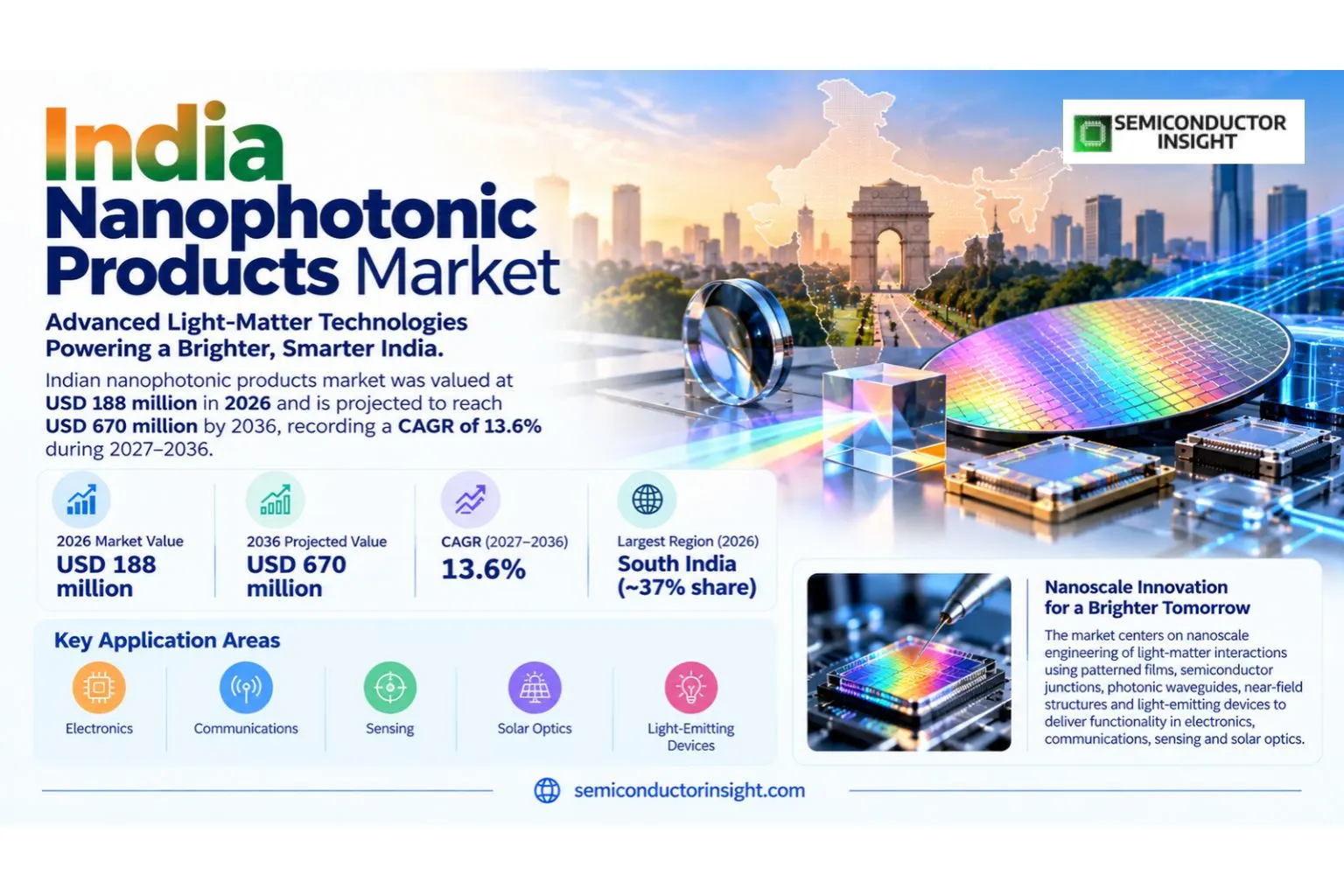
The Indian india nanophotonic products market was valued at USD 188 million in 2026 and is projected to reach USD 670 million by 2036, recording a CAGR of 13.6% during 2027–2036. South India was the largest region in 2026 at an estimated ~37% share. The market centers on nanoscale engineering of light-matter interactions using patterned films, semiconductor junctions, photonic waveguides, near-field structures and light-emitting devices to deliver functionality in electronics, communications, sensing and solar optics.
India Nanophotonic Products encompasses nanoscale engineering of light-matter interactions using patterned films, semiconductor junctions, photonic waveguides, near-field structures and light-emitting devices to deliver functionality in electronics, communications, sensing and solar optics. When evaluating india nanophotonic products ov_paras, the optical interaction carries or secures the functional payload, but the device must also include appropriately designed mechanical, electronic and service interfaces. Across India’s nanophotonic products ov_paras category, customers primarily pay for a qualified system that performs consistently in field conditions, rather than a technical principle demonstrated only at prototype level.
The defined commercial boundary includes nanostructure-enabled optical devices, optical switches, photonic sensors, qualified nanostructured LED and OLED components, specialized photovoltaic optical products and holographic memory elements sold into India; not all conventional LED lighting, all flat displays, the full renewable power system or telecom subscriber revenue. Among india nanophotonic products ov_paras buyers, this distinction prevents a finished datacenter, networking service or unrelated electronic product from being mistaken for direct sales of the specialized component. Within india nanophotonic products ov_paras, supplier comparisons are meaningful only when the invoiced product and its value contribution fall within the stated market boundary.
At the engineering level, nanoscale engineering of light-matter interactions using patterned films, semiconductor junctions, photonic waveguides, near-field structures and light-emitting devices to deliver functionality in electronics, communications, sensing and solar optics. For qualified india nanophotonic products ov_paras products, designing this technology for 2026 production requires material and mechanical stability, test coverage, procurement planning and the ability to identify a component that has begun to fail. During india nanophotonic products ov_paras procurement, qualification routines can be more costly than the core material in demanding installations.
Demand develops through Indian electronics assemblers, communications systems suppliers, display integrators, industrial lighting procurement agencies, semiconductor design laboratories and specialist optical-instrument buyers. In India’s nanophotonic products ov_paras setting, those purchasers differ in the volumes they order, the length of their evaluation cycle and the documentation they require. The leading applications are Entertainment, Consumer Electronics, Indicators And Signs, Lighting, Telecommunication, Non-Visual Applications; their spending patterns cannot simply be extrapolated from wider electronics or digital-storage demand.
Technology priorities are evolving toward more reliable and serviceable optical architectures. For india nanophotonic products ov_paras, nanoscale quantum well structures and semiconductor junction processing govern efficiency, color stability and thermal performance of specialized LED components. When evaluating india nanophotonic products ov_paras, indian lighting and display buyers can source finished devices widely, yet revenue attributable specifically to nanostructured optical products is narrower than the full LED lamp market. Across India’s nanophotonic products ov_paras category, the commercial challenge is to turn those technical characteristics into repeat purchasing, while addressing loss of compatibility, changing interfaces and the long-term economics of support.
Segment Analysis: By Type
The Indian india nanophotonic products market was valued at USD 188 million in 2026 and is projected to reach USD 670 million by 2036, recording a CAGR of 13.6% during 2027–2036. South India was the largest region in 2026 at an estimated ~37% share. The market centers on nanoscale engineering of light-matter interactions using patterned films, semiconductor junctions, photonic waveguides, near-field structures and light-emitting devices to deliver functionality in electronics, communications, sensing and solar optics.
| Type | Function | Market position |
|---|---|---|
| Light Emitting Diodes (Leds) | Within Light Emitting Diodes (Leds) configuration, nanoscale quantum well structures and semiconductor junction processing govern efficiency, color stability and thermal performance of specialized LED components. For qualified Light Emitting Diodes (Leds) configuration products, indian lighting and display buyers can source finished devices widely, yet revenue attributable specifically to nanostructured optical products is narrower than the full LED lamp market. During Light Emitting Diodes (Leds) configuration procurement, each product specification maps to a different material bill, operating environment and qualification procedure. Suppliers therefore need to establish how the Light Emitting Diodes (Leds) variant affects installation requirements and ongoing service. | Estimated ~27% of 2026 revenue and ~12.9% CAGR. Light Emitting Diodes (Leds) is the largest type by value, with demand linked to the particular requirements of its buyers. In the Light Emitting Diodes (Leds) configuration setting, nanoscale quantum well structures and semiconductor junction processing govern efficiency, color stability and thermal performance of specialized LED components. For Light Emitting Diodes (Leds) configuration, indian lighting and display buyers can source finished devices widely, yet revenue attributable specifically to nanostructured optical products is narrower than the full LED lamp market. When evaluating Light Emitting Diodes (Leds) configuration, procurement teams evaluate component availability, unit cost and the necessary test records. |
| Organic Leds (Oleds) | Organic emitting stacks and patterned thin-film deposition permit emissive display pixels and OLED lighting. MeitY-funded IIT Madras research explicitly addresses AMOLED manufacturing process capability, but research infrastructure and commercial panel production have different revenue implications. Across the Organic Leds (Oleds) configuration category, each product specification maps to a different material bill, operating environment and qualification procedure. Suppliers therefore need to establish how the Organic Leds (Oleds) variant affects installation requirements and ongoing service. | Estimated ~23% of 2026 revenue and ~14.7% CAGR. Organic Leds (Oleds) is a distinct product category, with demand linked to the particular requirements of its buyers. Among Organic Leds (Oleds) configuration buyers, organic emitting stacks and patterned thin-film deposition permit emissive display pixels and OLED lighting. Within Organic Leds (Oleds) configuration, meitY-funded IIT Madras research explicitly addresses AMOLED manufacturing process capability, but research infrastructure and commercial panel production have different revenue implications. For qualified Organic Leds (Oleds) configuration products, procurement teams evaluate component availability, unit cost and the necessary test records. |
| Near Field Optics | Near-field probes and subwavelength optical structures interact with evanescent fields over distances below conventional free-space diffraction scales. Research instruments, sensing and nanoscale characterization are specialist rather than broad-volume consumer demand; calibration and high-quality nanofabrication limit vendor options. During Near Field Optics configuration procurement, each product specification maps to a different material bill, operating environment and qualification procedure. Suppliers therefore need to establish how the Near Field Optics variant affects installation requirements and ongoing service. | Estimated ~9% of 2026 revenue and ~14.4% CAGR. Near Field Optics is a distinct product category, with demand linked to the particular requirements of its buyers. In the Near Field Optics configuration setting, near-field probes and subwavelength optical structures interact with evanescent fields over distances below conventional free-space diffraction scales. For Near Field Optics configuration, research instruments, sensing and nanoscale characterization are specialist rather than broad-volume consumer demand; calibration and high-quality nanofabrication limit vendor options. When evaluating Near Field Optics configuration, procurement teams evaluate component availability, unit cost and the necessary test records. |
| Photovoltaic Cells | Nanostructured surface treatments, thin films and optical trapping architectures can improve photovoltaic light absorption and conversion. Solar cell production is a much larger sector, so its entire cell and module turnover cannot be equated with the narrower nanophotonic product market. Across the Photovoltaic Cells configuration category, each product specification maps to a different material bill, operating environment and qualification procedure. Suppliers therefore need to establish how the Photovoltaic Cells variant affects installation requirements and ongoing service. | Estimated ~19% of 2026 revenue and ~12.2% CAGR. Photovoltaic Cells is a distinct product category, with demand linked to the particular requirements of its buyers. Among Photovoltaic Cells configuration buyers, nanostructured surface treatments, thin films and optical trapping architectures can improve photovoltaic light absorption and conversion. Within Photovoltaic Cells configuration, solar cell production is a much larger sector, so its entire cell and module turnover cannot be equated with the narrower nanophotonic product market. For qualified Photovoltaic Cells configuration products, procurement teams evaluate component availability, unit cost and the necessary test records. |
| Optical Switches | Integrated optical switches steer or modulate light through waveguide circuits or optoelectronic structures. Their buyer value lies in insertion loss, cross-talk, lifetime and coupling reproducibility, particularly for optical research benches and telecom equipment manufacturers. During Optical Switches configuration procurement, each product specification maps to a different material bill, operating environment and qualification procedure. Suppliers therefore need to establish how the Optical Switches variant affects installation requirements and ongoing service. | Estimated ~12% of 2026 revenue and ~14.3% CAGR. Optical Switches is a distinct product category, with demand linked to the particular requirements of its buyers. In the Optical Switches configuration setting, integrated optical switches steer or modulate light through waveguide circuits or optoelectronic structures. For Optical Switches configuration, their buyer value lies in insertion loss, cross-talk, lifetime and coupling reproducibility, particularly for optical research benches and telecom equipment manufacturers. When evaluating Optical Switches configuration, procurement teams evaluate component availability, unit cost and the necessary test records. |
| Optical Amplifiers | Optical amplifiers improve link power budgets in fibre networking systems, using gain components that must maintain wavelength response and low noise. Indian equipment integrators typically buy qualified subsystems, with revenue confined to the nanophotonic portion and not the entire optical network. Across the Optical Amplifiers configuration category, each product specification maps to a different material bill, operating environment and qualification procedure. Suppliers therefore need to establish how the Optical Amplifiers variant affects installation requirements and ongoing service. | Estimated ~8% of 2026 revenue and ~13.7% CAGR. Optical Amplifiers is a distinct product category, with demand linked to the particular requirements of its buyers. Among Optical Amplifiers configuration buyers, optical amplifiers improve link power budgets in fibre networking systems, using gain components that must maintain wavelength response and low noise. Within Optical Amplifiers configuration, indian equipment integrators typically buy qualified subsystems, with revenue confined to the nanophotonic portion and not the entire optical network. For qualified Optical Amplifiers configuration products, procurement teams evaluate component availability, unit cost and the necessary test records. |
| Holographic Memory | Holographic storage encodes data through optical interference within recording media or photonic architectures. Commercial adoption is limited compared with LED, OLED and telecommunication products; prototype evidence does not establish high-volume data storage purchases. During Holographic Memory configuration procurement, each product specification maps to a different material bill, operating environment and qualification procedure. Suppliers therefore need to establish how the Holographic Memory variant affects installation requirements and ongoing service. | Estimated ~2% of 2026 revenue and ~11.0% CAGR. Holographic Memory is a distinct product category, with demand linked to the particular requirements of its buyers. In the Holographic Memory configuration setting, holographic storage encodes data through optical interference within recording media or photonic architectures. For Holographic Memory configuration, commercial adoption is limited compared with LED, OLED and telecommunication products; prototype evidence does not establish high-volume data storage purchases. When evaluating Holographic Memory configuration, procurement teams evaluate component availability, unit cost and the necessary test records. |
Segment Analysis: By Application
Application segments are Entertainment, Consumer Electronics, Indicators And Signs, Lighting, Telecommunication, Non-Visual Applications. Consumer Electronics takes the largest estimated 2026 revenue share at ~29%, whereas Telecommunication is the fastest-growing application at ~14.6% CAGR. Across India’s nanophotonic products app category, channel structure, end-user servicing needs and purchasing cadence create distinct addressable opportunities despite shared underlying optical technologies. Among india nanophotonic products app buyers, in the application overview setting, an engineering advantage becomes a sale only after procurement teams review validation evidence, inventory risk, maintenance requirements and the operating economics of the intended deployment.
| Application | Demand characteristics |
|---|---|
| Entertainment | Estimated ~9% of 2026 revenue and ~14.0% CAGR. Stage displays, projection engines and event imaging use optical effects, but only qualified nanostructured emitters, switching elements or special photonics parts count toward this market. Customer budgets focus on reliability, color rendering and serviceability through integrators. Within Entertainment procurement, purchasers assess the entire cost of deploying and operating the optical function, including testability, compatible equipment and procurement lead times. |
| Consumer Electronics | Estimated ~29% of 2026 revenue and ~14.0% CAGR. For consumer electronics, patterned emitters, thin-film materials and optical sensors are specified at the component level inside phones and other devices. For qualified Consumer Electronics procurement products, production volumes are large but direct nanophotonic content varies widely by model and manufacturer, making component value distinct from finished phone or television revenue. During Consumer Electronics procurement procurement, purchasers assess the entire cost of deploying and operating the optical function, including testability, compatible equipment and procurement lead times. |
| Indicators And Signs | Estimated ~10% of 2026 revenue and ~12.8% CAGR. Industrial signs, vehicle indicators and illuminated wayfinding systems use efficient emitting devices, with nano-engineered layers influencing luminous efficacy and service life. Contracts prioritize compliance, thermal design and spare supply rather than frontier photonic chip features. In the Indicators And Signs procurement setting, purchasers assess the entire cost of deploying and operating the optical function, including testability, compatible equipment and procurement lead times. |
| Lighting | Estimated ~18% of 2026 revenue and ~11.8% CAGR. Commercial building lighting and public infrastructure retrofits procure LED and advanced optical products at substantial scale. Conventional lamps are not automatically classified as nanoscale photonic products; only the relevant specialized LED components or optical structures belong within this boundary. For Lighting procurement, purchasers assess the entire cost of deploying and operating the optical function, including testability, compatible equipment and procurement lead times. |
| Telecommunication | Estimated ~27% of 2026 revenue and ~14.6% CAGR. Fibre-optic access, backbone networks and datacenter links require qualified optical switches, amplifiers, transceivers and photonic components. BharatNet and TRAI broadband data identify infrastructure demand but not direct market revenue for nanostructured devices. When evaluating Telecommunication procurement, purchasers assess the entire cost of deploying and operating the optical function, including testability, compatible equipment and procurement lead times. |
| Non-Visual Applications | Estimated ~7% of 2026 revenue and ~13.0% CAGR. Specialist sensing, biomedical diagnostics, research instruments and agricultural optical controls use nanophotonic interactions beyond conventional imaging. Buyers emphasize repeatability and domain-specific validation, and orders may be small but technically demanding. Across the Non-Visual Applications procurement category, purchasers assess the entire cost of deploying and operating the optical function, including testability, compatible equipment and procurement lead times. |
The commercial channel is shaped by Indian electronics assemblers, communications systems suppliers, display integrators, industrial lighting procurement agencies, semiconductor design laboratories and specialist optical-instrument buyers. Among india nanophotonic products app buyers, direct equipment purchase, specialist distributor supply and OEM qualification have different order economics. Within india nanophotonic products app, volume can be won through stable specifications and documented reliability, while replacement sales depend on spare availability and retained interface compatibility over the 2027–2036 period.
Regional Analysis
South India leads India revenue with an estimated ~37% share in 2026. West India follows at ~25% and North India at ~19%. South India has the fastest growth at ~14.2% CAGR. For qualified india nanophotonic products regional products, regional purchases and supplier manufacturing footprints must be distinguished for market comparisons. During india nanophotonic products regional procurement, this matters for regional lead, because the technically feasible option must also be installable, serviceable and properly documented across the operating life of the equipment and its supporting software.
How do regional purchasing patterns differ in india nanophotonic products?
South India concentrates programmable silicon photonics research at IIT Madras and integrated electronics engineering around Bengaluru and Hyderabad, while West India links Maharashtra industrial demand with planned Gujarat compound-semiconductor LED production. North India combines national procurement, network operators and optical-fibre installations across Uttar Pradesh and the Delhi region. East India has newer semiconductor-related facilities in Odisha and optical laboratories in West Bengal, whereas Central and Northeast India reflects a developing technology supply chain in Assam and distributed industrial buyers. These locations are subregions of India, not independent international markets, and all percentages refer solely to the India national market.
| Region | Position | Growth outlook | Demand profile | What decides supplier selection |
|---|---|---|---|---|
| South India | Largest (~37%) | ~14.2% CAGR | In the South India’s nanophotonic products setting, south India combines the IIT Madras programmable PIC center, Bengaluru electronics design and Hyderabad photonic engineering. For South India’s nanophotonic products, research equipment purchases and pilot commercialization support the largest modeled subregional share of India-specific nanophotonic product revenue. Within South India, design wins may be awarded to chip producers offshore even when the finished optical equipment is installed locally, making customer qualification and international logistics decisive commercial factors. | Buyers in South India require engineering fit, credible warranty conditions, appropriate import arrangements, and a qualified local service path. For nanoscale engineering of light-matter interactions using patterned films, semiconductor junctions, photonic waveguides, near-field structures and light-emitting devices to deliver functionality in electronics, communications, sensing and solar optics, interface stability and the availability of replacement products can determine whether a promising order proceeds beyond initial evaluation. |
| West India | Second (~25%) | ~14.0% CAGR | West India includes Gujarat compound semiconductor display manufacturing commitments and Maharashtra electronics clusters. Its buyer mix spans optical transceiver components, engineered LED assemblies and photovoltaic devices. Within West India, design wins may be awarded to chip producers offshore even when the finished optical equipment is installed locally, making customer qualification and international logistics decisive commercial factors. | Buyers in West India require engineering fit, credible warranty conditions, appropriate import arrangements, and a qualified local service path. When evaluating West India’s nanophotonic products, for nanoscale engineering of light-matter interactions using patterned films, semiconductor junctions, photonic waveguides, near-field structures and light-emitting devices to deliver functionality in electronics, communications, sensing and solar optics, interface stability and the availability of replacement products can determine whether a promising order proceeds beyond initial evaluation. |
| North India | Third (~19%) | ~13.1% CAGR | North India has large optical-fibre network deployment requirements in Uttar Pradesh and national research centers near Delhi. Procurement concentrates on telecom modules, lighting products and electronic optical components through established channels. Within North India, design wins may be awarded to chip producers offshore even when the finished optical equipment is installed locally, making customer qualification and international logistics decisive commercial factors. | Buyers in North India require engineering fit, credible warranty conditions, appropriate import arrangements, and a qualified local service path. Across the North India’s nanophotonic products category, for nanoscale engineering of light-matter interactions using patterned films, semiconductor junctions, photonic waveguides, near-field structures and light-emitting devices to deliver functionality in electronics, communications, sensing and solar optics, interface stability and the availability of replacement products can determine whether a promising order proceeds beyond initial evaluation. |
| East India | Fourth (~11%) | ~12.4% CAGR | East India has semiconductor-related projects in Odisha and industrial electronics users in West Bengal. Demand is linked to pilot plant implementation, materials engineering and specialized optical testing rather than mass photonic wafer output. Within East India, design wins may be awarded to chip producers offshore even when the finished optical equipment is installed locally, making customer qualification and international logistics decisive commercial factors. | Buyers in East India require engineering fit, credible warranty conditions, appropriate import arrangements, and a qualified local service path. Among East India’s nanophotonic products buyers, for nanoscale engineering of light-matter interactions using patterned films, semiconductor junctions, photonic waveguides, near-field structures and light-emitting devices to deliver functionality in electronics, communications, sensing and solar optics, interface stability and the availability of replacement products can determine whether a promising order proceeds beyond initial evaluation. |
| Central & Northeast India | Fifth (~8%) | ~11.8% CAGR | Central and Northeast India contains Assam semiconductor packaging initiatives and growing rural fibre access. Smaller regional clusters procure photonic modules largely via nationwide integrators. Within Central & Northeast India, design wins may be awarded to chip producers offshore even when the finished optical equipment is installed locally, making customer qualification and international logistics decisive commercial factors. | Buyers in Central & Northeast India require engineering fit, credible warranty conditions, appropriate import arrangements, and a qualified local service path. Within Central & Northeast India’s nanophotonic products, for nanoscale engineering of light-matter interactions using patterned films, semiconductor junctions, photonic waveguides, near-field structures and light-emitting devices to deliver functionality in electronics, communications, sensing and solar optics, interface stability and the availability of replacement products can determine whether a promising order proceeds beyond initial evaluation. |
Competitive Landscape
India’s nanophotonic products ecosystem brings together photonic research organizations, electronics manufacturing firms, specialist optical-system integrators and emerging device developers. Public product disclosures do not confirm that every name in the historical profiled company list supplies commercially available nanophotonic devices. The clearest documented capacity additions are IIT Madras photonics prototyping and MeitY-supported display and component programs. Commercial comparisons therefore turn on actual qualified product lines, technology transfer, repeat orders and verified manufacturing capability, not inferred market shares from research project participation.
Tata Photonics and Plasmonics Technologies India Pvt. Ltd. illustrate different capabilities within the sector. Across India’s nanophotonic products supplier competition category, their product portfolios, production locations and support arrangements cannot be assumed identical. Among india nanophotonic products supplier competition buyers, procurement departments typically request specification sheets, samples, aging or thermal data and a long-term sourcing plan before designating a manufacturing source for a multi-year contract. Within india nanophotonic products supplier competition, a commercial evaluation of manufacturer capability therefore compares the cost of qualified materials, process yield, lead times, quality assurance and post-installation support rather than product specifications alone.
Indian Institute of Photonic Technology, Photonics Technology Limited, Nanophotonics India Ltd., Advanced NanoTech Lab, Bharat Photonics appear in the wider manufacturer and distributor field. For qualified india nanophotonic products supplier competition products, the roles of those entities require separation: media production, component housing manufacture, systems integration and distribution do not produce the same category of invoice. During india nanophotonic products supplier competition procurement, market rivalry occurs at the level of the particular sold device, not across unrelated corporate divisions.
Other suppliers and historical business names include Bharat Photonics, Nano Optoelectronics, Quantum Photonics Innovations, Nano Solutions. In India’s nanophotonic products supplier competition setting, legacy corporate names and regional branches may persist in industry directories, while actual current production must be checked against updated company disclosures. For india nanophotonic products supplier competition, product-life-cycle changes can alter sourcing qualification even if an installed system continues to function with existing spare inventories.
When evaluating india nanophotonic products supplier competition, for 2027–2036, vendor differentiation will depend on manufacturing yield, documentation, reliable delivery and compatibility with demanding optical interfaces. Across India’s nanophotonic products supplier competition category, price competition may intensify in mature configurations, whereas new package geometries or archival media offer specialized margins. Among india nanophotonic products supplier competition buyers, a customer switching supplier must weigh requalification, sample validation and operational interruption against lower unit costs. Within india nanophotonic products supplier competition, the 2027–2036 opportunity in competitive economics is linked to deployment timing and customer acceptance, with supplier selection reflecting reliability, supply continuity, interface requirements and actual unit economics.
Tier structure
| Tier | Companies | Basis of competition |
|---|---|---|
| Tier 1 | Commercial LED/OLED and optical-component device suppliers | Buyers of specialist emitters, switches, amplifiers and optical components require current technical catalogs, part traceability, repeatable shipment capability and service contracts. National electronic component programs broaden the potential supplier base, but approved projects and research grants do not prove product-specific sales of nanophotonic devices. The commercial tier is defined by active qualifying shipments rather than unpublished rankings. |
| Tier 2 | Systems integrators and electronics manufacturing service providers | India-based electronics assembly and module integrators combine optical devices with electronic drive circuits, display structures and network interfaces. Their invoices may include complete systems, with only the directly attributable nano-optical content counted within this market. Qualification, import logistics and local test capability determine whether a given optical product can be sourced and maintained over its design life. |
| Tier 3 | Research laboratories and historically profiled entities | Universities, government-funded photonics laboratories and historical company-list entries occupy the broader technology ecosystem. IIT Madras operates a documented silicon-photonics research and test platform. Other listed entities require verification of their legal status, catalog and active customer relationships before being treated as revenue-ranked suppliers; research activity does not establish a commercial market share. |
Key companies profiled
- Tata Photonics
- Plasmonics Technologies India Pvt. Ltd.
- Indian Institute of Photonic Technology
- Photonics Technology Limited
- Nanophotonics India Ltd.
- Advanced NanoTech Lab
- Bharat Photonics
- Nano Optoelectronics
- Quantum Photonics Innovations
- Nano Solutions
Production Capacity Analysis
Production capacity relies on specialized manufacturing and testing for nanoscale engineering of light-matter interactions using patterned films, semiconductor junctions, photonic waveguides, near-field structures and light-emitting devices to deliver functionality in electronics, communications, sensing and solar optics. For qualified india nanophotonic products prod products, effective output is constrained by qualified material lots, process yield, equipment availability and completion of electrical, optical and environmental tests. During india nanophotonic products prod procurement, announced industrial capability should not be equated automatically with installed sales or usable nameplate capacity.
Initial manufacturing operations include nanoscale engineering of light-matter interactions using patterned films, semiconductor junctions, photonic waveguides, near-field structures and light-emitting devices to deliver functionality in electronics, communications, sensing and solar optics. In India’s nanophotonic products prod setting, yield is influenced by each fabrication and assembly stage, while changes in materials or process equipment can require formal requalification. Japan, China and other South India manufacturing centers support considerable supplier capacity, although customer purchasing decisions may originate elsewhere.
For india nanophotonic products prod, diversified capacity can reduce country-of-origin exposure and help supply different qualification requirements. When evaluating india nanophotonic products prod, however, transferring tooling and process knowledge between plants takes time, and products made in new locations may require fresh qualification. Across India’s nanophotonic products prod category, strong inventory controls and component traceability are important during a period of changing designs and volatile customer orders. Among india nanophotonic products prod buyers, this matters for capacity diversification, because the technically feasible option must also be installable, serviceable and properly documented across the operating life of the equipment and its supporting software.
Within india nanophotonic products prod, upstream constraints include materials, specialized assembly equipment and trained optical manufacturing staff. For india nanophotonic products, packaging, testing and maintenance infrastructure shape the ability to convert a technical design into reproducible revenue. For qualified india nanophotonic products prod products, companies should distinguish capacity for direct in-scope products from headline capacity for the much larger adjacent electronics manufacturing market. During india nanophotonic products prod procurement, a commercial evaluation of capacity bottlenecks therefore compares the cost of qualified materials, process yield, lead times, quality assurance and post-installation support rather than product specifications alone.
Market Dynamics
Demand is driven by domestic optical connectivity and fibre network upgrades and led, oled and micro-led display component development. In India’s nanophotonic products lead setting, growth depends on matching the optical product to qualification requirements, logistics and total ownership cost. Supplier economics also reflect the negative impact of limited qualified domestic nanoscale fabrication capacity, particularly when customers require long operational support.
MARKET DRIVERS
Drivers Impact Analysis*
| Driver | (~) % impact on CAGR forecast | Geographic relevance | Impact timeline |
|---|---|---|---|
| Domestic optical connectivity and fibre network upgrades | +1.8% | South India | 2027–2036 |
| LED, OLED and micro-LED display component development | +1.4% | Global | 2028–2034 |
| Electronics manufacturing localisation schemes | +1.1% | West India | 2027–2031 |
| Silicon photonics research and test infrastructure | +0.9% | North India | 2029–2036 |
| Specialist nano-optical sensors and laboratories | +0.7% | Global | 2028–2035 |
Domestic optical connectivity and fibre network upgrades
Domestic optical connectivity and fibre network upgrades supports specialized purchases for India nanophotonic products. nanoscale engineering of light-matter interactions using patterned films, semiconductor junctions, photonic waveguides, near-field structures and light-emitting devices to deliver functionality in electronics, communications, sensing and solar optics must be integrated into customer processes, inspected and supported. For india nanophotonic products drivers, the growth effect is directional, not a separate addition to the headline CAGR. When evaluating india nanophotonic products drivers, actual adoption depends on confirmed orders, service requirements and the lifecycle of equipment already installed.
LED, OLED and micro-LED display component development
LED, OLED and micro-LED display component development supports specialized purchases for India nanophotonic products. nanoscale engineering of light-matter interactions using patterned films, semiconductor junctions, photonic waveguides, near-field structures and light-emitting devices to deliver functionality in electronics, communications, sensing and solar optics must be integrated into customer processes, inspected and supported. Across India’s nanophotonic products drivers category, the growth effect is directional, not a separate addition to the headline CAGR. Among india nanophotonic products drivers buyers, actual adoption depends on confirmed orders, service requirements and the lifecycle of equipment already installed.
Electronics manufacturing localisation schemes
Electronics manufacturing localisation schemes supports specialized purchases for India nanophotonic products. nanoscale engineering of light-matter interactions using patterned films, semiconductor junctions, photonic waveguides, near-field structures and light-emitting devices to deliver functionality in electronics, communications, sensing and solar optics must be integrated into customer processes, inspected and supported. Within india nanophotonic products drivers, the growth effect is directional, not a separate addition to the headline CAGR. For qualified india nanophotonic products drivers products, actual adoption depends on confirmed orders, service requirements and the lifecycle of equipment already installed.
Silicon photonics research and test infrastructure
Silicon photonics research and test infrastructure supports specialized purchases for India nanophotonic products. nanoscale engineering of light-matter interactions using patterned films, semiconductor junctions, photonic waveguides, near-field structures and light-emitting devices to deliver functionality in electronics, communications, sensing and solar optics must be integrated into customer processes, inspected and supported. During india nanophotonic products drivers procurement, the growth effect is directional, not a separate addition to the headline CAGR. In India’s nanophotonic products drivers setting, actual adoption depends on confirmed orders, service requirements and the lifecycle of equipment already installed.
MARKET RESTRAINTS
Restraints Impact Analysis*
| Restraint | (~) % impact on CAGR forecast | Geographic relevance | Impact timeline |
|---|---|---|---|
| Limited qualified domestic nanoscale fabrication capacity | −1.5% | Global | 2027–2036 |
| Dependence on imported lithography and deposition tools | −1.1% | North India and West India | 2027–2034 |
| Difficult product qualification across diverse photonic types | −0.8% | South India | 2028–2035 |
| Misclassification of conventional LED and photovoltaic sales | −0.6% | Global | 2029–2036 |
Limited qualified domestic nanoscale fabrication capacity
Limited qualified domestic nanoscale fabrication capacity increases the effort required to qualify or replace india nanophotonic products. For india nanophotonic products restraints, a technical disadvantage can translate into delayed procurement, more maintenance work or poorer economics for the user. When evaluating india nanophotonic products restraints, suppliers that demonstrate stable performance and clear service processes may offset some of this commercial risk, but the constraint remains important for 2027–2036 forecasts. The 2027–2036 opportunity in Limited qualified domestic nanoscale fabrication capacity restraint is linked to deployment timing and customer acceptance, with supplier selection reflecting reliability, supply continuity, interface requirements and actual unit economics.
Dependence on imported lithography and deposition tools
Dependence on imported lithography and deposition tools increases the effort required to qualify or replace india nanophotonic products. Across India’s nanophotonic products restraints category, a technical disadvantage can translate into delayed procurement, more maintenance work or poorer economics for the user. Among india nanophotonic products restraints buyers, suppliers that demonstrate stable performance and clear service processes may offset some of this commercial risk, but the constraint remains important for 2027–2036 forecasts. For Dependence on imported lithography and deposition tools restraint in 2027, the purchase decision depends on explicit equipment compatibility, verifiable component performance and whether the supplier can sustain replacement support throughout the planned service interval.
Difficult product qualification across diverse photonic types
Difficult product qualification across diverse photonic types increases the effort required to qualify or replace india nanophotonic products. Within india nanophotonic products restraints, a technical disadvantage can translate into delayed procurement, more maintenance work or poorer economics for the user. For qualified india nanophotonic products restraints products, suppliers that demonstrate stable performance and clear service processes may offset some of this commercial risk, but the constraint remains important for 2027–2036 forecasts. In the Difficult product qualification across diverse photonic types restraint setting, an engineering advantage becomes a sale only after procurement teams review validation evidence, inventory risk, maintenance requirements and the operating economics of the intended deployment.
Misclassification of conventional LED and photovoltaic sales
Misclassification of conventional LED and photovoltaic sales increases the effort required to qualify or replace india nanophotonic products. During india nanophotonic products restraints procurement, a technical disadvantage can translate into delayed procurement, more maintenance work or poorer economics for the user. In India’s nanophotonic products restraints setting, suppliers that demonstrate stable performance and clear service processes may offset some of this commercial risk, but the constraint remains important for 2027–2036 forecasts. This matters for Misclassification of conventional LED and photovoltaic sales restraint, because the technically feasible option must also be installable, serviceable and properly documented across the operating life of the equipment and its supporting software.
MARKET OPPORTUNITIES
Programmable silicon photonic test and PDK services
Programmable silicon photonic test and PDK services creates an opportunity to improve deployment or the supplier value proposition. The relevant engineering work concerns nanoscale engineering of light-matter interactions using patterned films, semiconductor junctions, photonic waveguides, near-field structures and light-emitting devices to deliver functionality in electronics, communications, sensing and solar optics. For india nanophotonic products opps, buyers still require evidence of stable operation, a practical purchasing channel, training and a predictable replacement schedule. When evaluating india nanophotonic products opps, the commercial impact is strongest where those requirements can be standardized across several customers.
Specialized GaN mini- and micro-LED displays
Specialized GaN mini- and micro-LED displays creates an opportunity to improve deployment or the supplier value proposition. Across India’s nanophotonic products opps category, the relevant engineering work concerns nanoscale engineering of light-matter interactions using patterned films, semiconductor junctions, photonic waveguides, near-field structures and light-emitting devices to deliver functionality in electronics, communications, sensing and solar optics. Among india nanophotonic products opps buyers, buyers still require evidence of stable operation, a practical purchasing channel, training and a predictable replacement schedule. Within india nanophotonic products opps, the commercial impact is strongest where those requirements can be standardized across several customers.
Optical modules for fibre and datacenter networks
Optical modules for fibre and datacenter networks creates an opportunity to improve deployment or the supplier value proposition. For qualified india nanophotonic products opps products, the relevant engineering work concerns nanoscale engineering of light-matter interactions using patterned films, semiconductor junctions, photonic waveguides, near-field structures and light-emitting devices to deliver functionality in electronics, communications, sensing and solar optics. During india nanophotonic products opps procurement, buyers still require evidence of stable operation, a practical purchasing channel, training and a predictable replacement schedule. In India’s nanophotonic products opps setting, the commercial impact is strongest where those requirements can be standardized across several customers.
Nanoscale biomedical and industrial sensing
Nanoscale biomedical and industrial sensing creates an opportunity to improve deployment or the supplier value proposition. For india nanophotonic products opps, the relevant engineering work concerns nanoscale engineering of light-matter interactions using patterned films, semiconductor junctions, photonic waveguides, near-field structures and light-emitting devices to deliver functionality in electronics, communications, sensing and solar optics. When evaluating india nanophotonic products opps, buyers still require evidence of stable operation, a practical purchasing channel, training and a predictable replacement schedule. Across India’s nanophotonic products opps category, the commercial impact is strongest where those requirements can be standardized across several customers.
Supply Chain Analysis
The supply chain links specialized raw materials, device fabrication, verification, system integration and servicing for India nanophotonic products. A failure at any stage can invalidate the qualified end product. Among india nanophotonic products supply buyers, vendor selection is therefore affected by more than selling price: replacement-component availability, inspection data, lead time and the ability to support legacy interfaces are commercially significant.
Upstream materials. For india nanophotonic products supply, materials and optical substrates required for nanoscale engineering of light-matter interactions using patterned films, semiconductor junctions, photonic waveguides, near-field structures and light-emitting devices to deliver functionality in electronics, communications, sensing and solar optics; inspection before assembly. For india nanophotonic products, controlling change across this stage enables traceability, reliability and repeatable delivery. When evaluating india nanophotonic products supply, purchasing teams demand technical records that explain product behavior and clarify responsibility if a component fails after deployment.
Manufacturing. Fabrication, alignment, sealing or recording operations matched to the market boundary. Across India’s nanophotonic products supply category, for india nanophotonic products, controlling change across this stage enables traceability, reliability and repeatable delivery. Among india nanophotonic products supply buyers, purchasing teams demand technical records that explain product behavior and clarify responsibility if a component fails after deployment. For Manufacturing chain in 2027, the purchase decision depends on explicit equipment compatibility, verifiable component performance and whether the supplier can sustain replacement support throughout the planned service interval.
Channels. Within india nanophotonic products supply, oEM engineering contracts, technical distributors and integrated storage or optical equipment vendors. For qualified india nanophotonic products supply products, for india nanophotonic products, controlling change across this stage enables traceability, reliability and repeatable delivery. During india nanophotonic products supply procurement, purchasing teams demand technical records that explain product behavior and clarify responsibility if a component fails after deployment. In the Channels chain setting, an engineering advantage becomes a sale only after procurement teams review validation evidence, inventory risk, maintenance requirements and the operating economics of the intended deployment.
Downstream users. In India’s nanophotonic products supply setting, indian electronics assemblers, communications systems suppliers, display integrators, industrial lighting procurement agencies, semiconductor design laboratories and specialist optical-instrument buyers; qualification, deployment and lifecycle support. For india nanophotonic products supply, for india nanophotonic products, controlling change across this stage enables traceability, reliability and repeatable delivery. When evaluating india nanophotonic products supply, purchasing teams demand technical records that explain product behavior and clarify responsibility if a component fails after deployment within its distinct operating requirements.
Recent Developments
- 17 August 2026 Published
The Ministry of Electronics and Information Technology reported 106 approved electronics component projects, with 38 operating plants and 16 more at advanced construction or equipment-installation stages. This expansion could improve assembly and packaging capacity for specialized photonic components, although total electronics investments are not equal to nano-optics product revenue. This matters for India Nanophotonic Products development 17 August 2026, because the technically feasible option must also be installable, serviceable and properly documented across the operating life of the equipment and its supporting software. Source - 14 July 2026 Announced
The IIT Madras photonics centre met SilTerra Malaysia for two days in July 2026 to discuss its domestic process design kit, multi-project wafer access and future heterogenous three-dimensional photonics packaging. The discussions offer a route toward production-ready engineering services rather than immediate high-volume chip shipments in India. A commercial evaluation of India Nanophotonic Products development 14 July 2026 therefore compares the cost of qualified materials, process yield, lead times, quality assurance and post-installation support rather than product specifications alone. Source - 5 May 2026 Approved
The Union Cabinet approved Gujarat projects including a compound-semiconductor Mini/Micro-LED display facility and semiconductor packaging capacity with investment of about INR 3,936 crore. Nanoengineered light emitters may benefit as capital equipment is installed, but the approval should be interpreted as planned capacity rather than realized device revenue. The 2027–2036 opportunity in India Nanophotonic Products development 5 May 2026 is linked to deployment timing and customer acceptance, with supplier selection reflecting reliability, supply continuity, interface requirements and actual unit economics. Source - 24 April 2026 Announced
MeitY and IIT Madras launched a silicon photonics process design kit and a packaged programmable photonic IC test engine for shared national use. The infrastructure gives researchers a better path from circuit design toward measurement and packaging, reducing prototyping barriers without itself establishing a sold-device market share. For India Nanophotonic Products development 24 April 2026 in 2032, the purchase decision depends on explicit equipment compatibility, verifiable component performance and whether the supplier can sustain replacement support throughout the planned service interval. Source - 18 March 2026 Announced
The Ministry of New and Renewable Energy expanded the Approved List of Models and Manufacturers framework to ingots and wafers, with implementation from June 2028. Stronger photovoltaic supply-chain qualification may indirectly affect nanostructured optical materials, but broad solar investment must not be attributed in full to nanophotonic products. In India’s nanophotonic products development 18 March 2026 setting, an engineering advantage becomes a sale only after procurement teams review validation evidence, inventory risk, maintenance requirements and the operating economics of the intended deployment. Source - 11 March 2026 Published
A Ministry of Electronics and Information Technology statement identified camera modules and optical transceivers among component categories under the Electronics Components Manufacturing Scheme. Optical integration can create downstream demand for nanoengineered devices, while project approvals and manufacturing incentives remain separate economic measures. This matters for India Nanophotonic Products development 11 March 2026, because the technically feasible option must also be installable, serviceable and properly documented across the operating life of the equipment and its supporting software. Source - 12 February 2026 Published
The Ministry of Communications reported more than 214,000 gram panchayats connected under BharatNet and progress toward universal broadband access. Optical network deployment is a demand indicator for relevant active photonic parts, though the value of fibre installation and subscriber services lies outside this device market. A commercial evaluation of India Nanophotonic Products development 12 February 2026 therefore compares the cost of qualified materials, process yield, lead times, quality assurance and post-installation support rather than product specifications alone. Source
REPORT SCOPE & SEGMENTATION
| Attribute | Details |
|---|---|
| Study Period | 2021–2036 |
| Base Year | 2026 |
| Estimated Year | 2027 |
| Forecast Period | 2027–2036 |
| Historical Period | 2021–2025 |
| Base Year Market Size | USD 188 million |
| Estimated Year Market Size | USD 213 million |
| Forecast Year Market Size | USD 670 million |
| CAGR | 13.6% |
| Unit | USD million |
| Market Definition | nanostructure-enabled optical devices, optical switches, photonic sensors, qualified nanostructured LED and OLED components, specialized photovoltaic optical products and holographic memory elements sold into India; not all conventional LED lighting, all flat displays, the full renewable power system or telecom subscriber revenue |
| By Type | Light Emitting Diodes (Leds) · Organic Leds (Oleds) · Near Field Optics · Photovoltaic Cells · Optical Switches · Optical Amplifiers · Holographic Memory |
| By Application | Entertainment · Consumer Electronics · Indicators And Signs · Lighting · Telecommunication · Non-Visual Applications |
| By Region | India national market only. Five subregional allocations: South India, West India, North India, East India, and Central & Northeast India, with sales attributed by domestic buyer location rather than foreign manufacturing origin. South IndiaTamil Nadu · Karnataka · Telangana · Kerala West IndiaMaharashtra · Gujarat · Goa North IndiaDelhi NCR · Uttar Pradesh · Punjab East IndiaOdisha · West Bengal · Bihar Central & Northeast IndiaAssam · Madhya Pradesh · Chhattisgarh |
| Key Companies Profiled | Tata Photonics; Plasmonics Technologies India Pvt. Ltd.; Indian Institute of Photonic Technology; Photonics Technology Limited; Nanophotonics India Ltd.; Advanced NanoTech Lab; Bharat Photonics; Nano Optoelectronics; Quantum Photonics Innovations; Nano Solutions |
| Customization Scope | Supplier, type, application and regional price analysis for India nanophotonic products; estimated market shares in 2026 and differentiated growth paths for 2027–2036. |
Frequently Asked Questions
What is India’s nanophotonic products market size?
India’s nanophotonic products market is valued at USD 188 million in 2026 and is forecast to reach USD 670 million by 2036, with 13.6% CAGR during 2027–2036. Across India’s nanophotonic products buyer questions category, the demand boundary is specific to the optical equipment and technology defined here rather than the full revenue of all data-center, media, automotive or electronics systems.
Which geographic region is the largest market?
South India is the leading 2026 regional market with an estimated ~37% of revenue. West India and North India follow at ~25% and ~19%, respectively. Among india nanophotonic products buyer questions buyers, differences in OEM manufacturing locations and customer purchasing geography can otherwise distort region comparisons. The 2027–2036 opportunity in FAQ 2 is linked to deployment timing and customer acceptance, with supplier selection reflecting reliability, supply continuity, interface requirements and actual unit economics.
Which region has the fastest growth rate?
South India has the highest estimated regional expansion at ~14.2% CAGR through 2036. Within india nanophotonic products buyer questions, south India combines the IIT Madras programmable PIC center, Bengaluru electronics design and Hyderabad photonic engineering. For qualified india nanophotonic products buyer questions products, research equipment purchases and pilot commercialization support the largest modeled subregional share of India-specific nanophotonic product revenue. During india nanophotonic products buyer questions procurement, the rate is linked to equipment deployment, supplier qualification and the technology mix, rather than broad GDP growth alone.
Which type holds the largest revenue share?
Light Emitting Diodes (Leds) represents an estimated ~27% of the 2026 market. In India’s nanophotonic products buyer questions setting, nanoscale quantum well structures and semiconductor junction processing govern efficiency, color stability and thermal performance of specialized LED components. For india nanophotonic products buyer questions, indian lighting and display buyers can source finished devices widely, yet revenue attributable specifically to nanostructured optical products is narrower than the full LED lamp market. When evaluating india nanophotonic products buyer questions, buyers need to verify its performance, equipment compatibility and the available delivery chain before treating it as an interchangeable substitute for another optical format.
Which type is projected to expand fastest?
Organic Leds (Oleds) carries the strongest estimated type growth at ~14.7% CAGR, from around ~23% of 2026 revenue. Across India’s nanophotonic products buyer questions category, the product mix changes as users adopt performance-enhancing configurations, but engineering qualification and lifecycle servicing determine how quickly that potential converts into orders. For FAQ 5 in 2027, the purchase decision depends on explicit equipment compatibility, verifiable component performance and whether the supplier can sustain replacement support throughout the planned service interval.
What is the leading application?
Consumer Electronics is the largest application at approximately ~29% of 2026 revenue. Among india nanophotonic products buyer questions buyers, displays, imaging and mobile hardware create a broad destination for efficient LEDs, OLED components and nanoscale optical materials. Within india nanophotonic products buyer questions, production volumes are large but direct nanophotonic content varies widely by model and manufacturer, making component value distinct from finished phone or television revenue. For qualified india nanophotonic products buyer questions products, procurement specifications depend on actual operating conditions; total revenue in the wider user industry is not a direct proxy for the value of optical equipment purchased.
Which application grows fastest?
Telecommunication is projected to grow at ~14.6% CAGR from approximately ~27% of 2026 revenue. Indian telecommunications operators purchase optical equipment for new fibre links, while module producers qualify switches, amplifiers and photonic interfaces against the deployed transport standards. During india nanophotonic products buyer questions procurement, bharatNet and TRAI broadband data identify infrastructure demand but not direct market revenue for nanostructured devices. In India’s nanophotonic products buyer questions setting, growth is affected by price changes and supplier qualification as well as physical unit demand.
Which companies are included?
The profiled market participants include Tata Photonics, Plasmonics Technologies India Pvt. Ltd., Indian Institute of Photonic Technology, Photonics Technology Limited, Nanophotonics India Ltd., Advanced NanoTech Lab. For india nanophotonic products buyer questions, these companies may operate in different parts of the value chain and in some cases retain historical naming. When evaluating india nanophotonic products buyer questions, comparisons need to distinguish direct in-scope equipment manufacturing from distribution, materials and wider group revenues.
What restrains adoption?
Limited qualified domestic nanoscale fabrication capacity is a notable limitation, alongside dependence on imported lithography and deposition tools. Customers must also examine service cost, quality-control requirements and purchasing terms. Across India’s nanophotonic products buyer questions category, technical improvement will not necessarily produce corresponding annual revenue growth without reproducible production and access to qualified buyers. In the FAQ 9 setting, an engineering advantage becomes a sale only after procurement teams review validation evidence, inventory risk, maintenance requirements and the operating economics of the intended deployment.
What is the study period and segmentation scope?
Among india nanophotonic products buyer questions buyers, the base year is 2026, the estimated year is 2027, and the forecast runs through 2036 with historical context from 2021–2025. Segmentation by type covers Light Emitting Diodes (Leds), Organic Leds (Oleds), Near Field Optics, Photovoltaic Cells, Optical Switches, Optical Amplifiers, Holographic Memory and by application covers Entertainment, Consumer Electronics, Indicators And Signs, Lighting, Telecommunication, Non-Visual Applications. Five geographic regions are included.
Research Sources & Evidence Base

Get Sample Report PDF for Exclusive Insights
Report Sample Includes
- Table of Contents
- List of Tables & Figures
- Charts, Research Methodology, and more...
 Download Sample Report PDF