Key Statistics
Key Takeaways
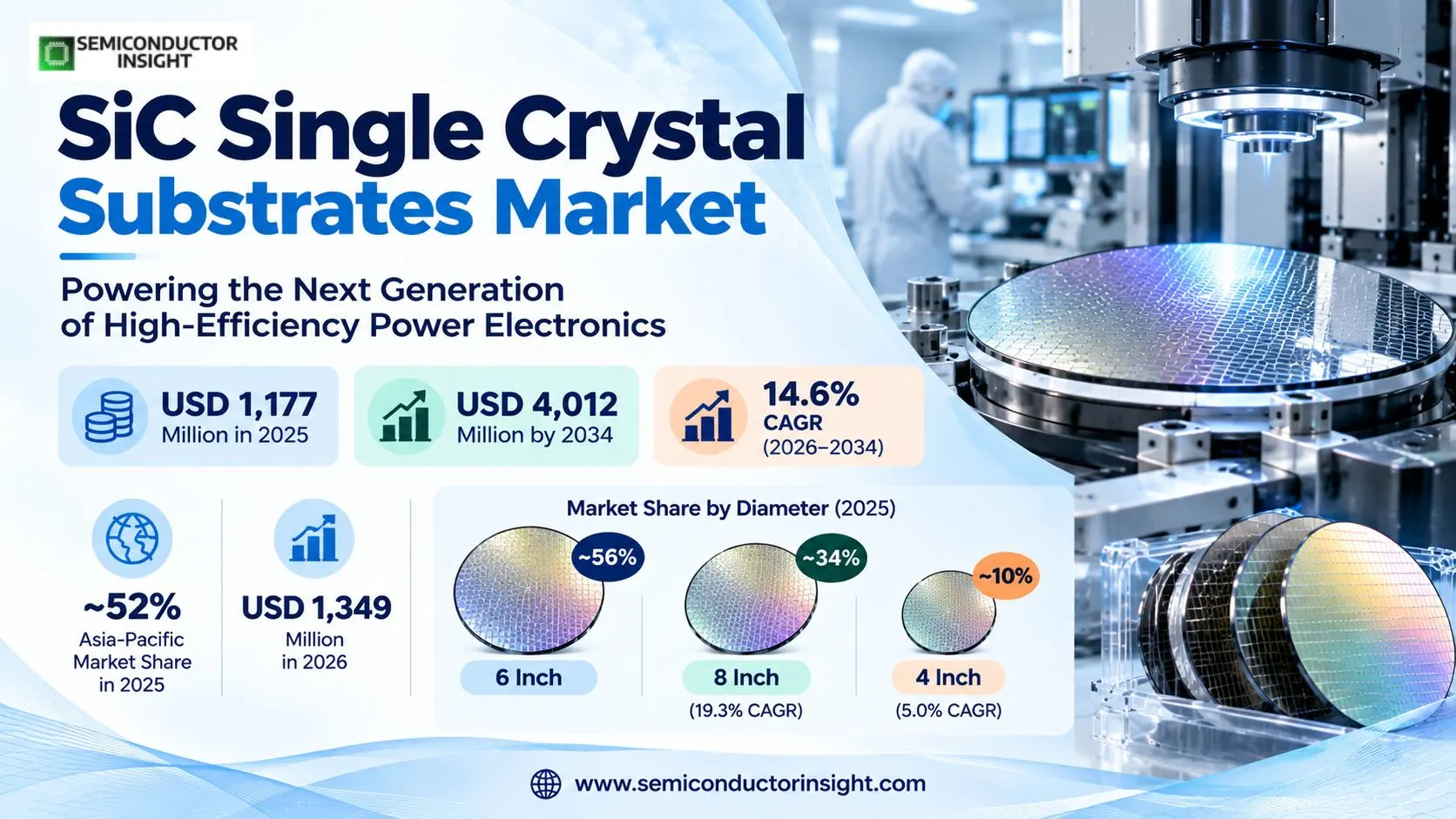
- Market trajectory: The global SiC single crystal substrates market was valued at USD 1,177 million in 2025 and is projected to reach USD 4,012 million in 2034, implying a 14.6% CAGR for 2026–2034; the 2026 estimate is USD 1,349 million.
- Diameter transition: The 6 Inch class retains an estimated ~56% of 2025 revenue, while the 8 Inch class holds ~34% and expands faster as power-device factories qualify 200 mm material for high-voltage switching architectures.
- Application concentration: Power Device manufacturing represents an estimated ~70% of substrate purchases; Wireless Infrastructure takes ~15%, Electronics & Optoelectronics ~11%, and the remaining ~4% serves specialized laboratory and industrial needs.
- Regional balance: Asia-Pacific leads with ~52% of 2025 sales, followed by Europe at ~20%, North America at ~19%, the Middle East & Africa at ~5%, and South America at ~4%.
- Technology economics: Crystal dislocation density, boule utilization, wafer bow, thickness variation and epitaxial compatibility determine whether the larger 200 mm format delivers a genuine cost-per-good-die advantage over established 150 mm lines.
- Supplier positioning: Wolfspeed, Coherent, ROHM Group through SiCrystal, SK Siltron CSS, Resonac and Chinese crystal specialists compete through quality assurance, wafer qualification history, multi-year supply agreements and vertically integrated capabilities.
SiC Single Crystal Substrates Market Overview
SiC single crystal substrates market reached USD 1,177 million in 2025 and is forecast to total USD 4,012 million by 2034, corresponding to a 14.6% CAGR during 2026–2034. Asia-Pacific accounts for the largest modeled 2025 regional share at ~52%, while the 2026 market estimate is USD 1,349 million.
A silicon carbide single-crystal substrate is a sliced, ground and polished wafer produced from a bulk SiC crystal, most commonly the 4H polytype used for high-performance power electronics. Unlike a conventional silicon starting wafer, the material supports devices operating under elevated electric fields and junction temperatures, but its production depends on carefully controlled physical-vapor-transport crystal growth. The merchant product is the qualified crystalline starting surface, not the completed transistor or converter. Manufacturers specify diameter, crystal orientation, doping, surface roughness, thickness uniformity and defect metrics before approving a substrate lot.
The commercial boundary includes 4 Inch, 6 Inch and 8 Inch SiC single-crystal substrate wafers destined for Power Device, Electronics & Optoelectronics, Wireless Infrastructure and other specialized fabrication. It excludes finished MOSFETs, packaged rectifiers, power modules, vehicle inverters, radio amplifiers and separately sold epitaxial processing services. Integrated producers may consume some wafers internally, but internal transfers are not added again as independent merchant sales. This distinction matters because one boule can support multiple processing stages whose gross transaction values cannot simply be summed without double counting.
Wafer diameter is an unusually important variable in this material category. A 200 mm circle has roughly 1.78 times the geometric area of a 150 mm circle before edge exclusion, so its potential die output is attractive for customers planning larger power-device factories. Actual usable area depends on crystal defects, bow, grinding damage and epitaxial yield; a nominal increase in surface area does not guarantee proportional good-die output. Suppliers that can deliver stable lots over several quarters obtain stronger customer qualification positions than entrants offering attractive spot prices but variable defect maps.
The 2025 market remains weighted toward 150 mm substrates, but the procurement conversation has shifted from diameter availability to predictable cost per electrically acceptable device. Automotive inverter programmes demand traceability and long support horizons, whereas industrial conversion customers can be more flexible about qualification cycles. Radio-frequency uses sometimes require semi-insulating material instead of conductive n-type substrates, so customers assess resistivity and crystalline quality differently. These divergent end markets make a single average wafer price misleading unless the wafer grade, diameter and surface specification are stated together.
Expansion is being shaped by an interaction between new crystal furnaces, customer multi-sourcing policies and demand from high-voltage power electronics. New capacity does not instantly translate into sales: growing an acceptable boule, slicing it without excessive loss, preparing an epitaxy-ready surface and passing customer device trials are distinct bottlenecks. The market therefore rewards process learning, inspection capability and stable quality systems alongside nameplate wafer capacity. Investors and procurement teams should distinguish substrate announcements, capital budgets and downstream device demand from realized wafer revenue.
Segment Analysis: By Type
By diameter, 6 Inch, 8 Inch and 4 Inch substrates form the three publisher-defined classes. The 6 Inch category is the largest at ~56% of 2025 revenue, the 8 Inch category contributes ~34% and is modeled to expand at ~19.3% CAGR, and legacy 4 Inch wafers represent ~10% with slower ~5.0% annual growth. Diameter selection influences both equipment compatibility and defect-screening cost.
| Diameter | Technical and purchasing characteristics | Market position |
|---|---|---|
| 4 Inch | The 100 mm class remains relevant in selected specialty production, research programmes and older RF-oriented processes that do not justify immediate equipment conversion. Small-diameter tooling is widely understood and a buyer may retain the format when wafer throughput is not the main constraint. Qualification can prioritize semi-insulating behavior, flatness and lot continuity over absolute surface area, particularly where device designs were established years earlier. | Estimated ~10% of 2025 substrate revenue and a modeled ~5.0% CAGR. This segment has a limited expansion pipeline because new high-volume power factories generally prefer 150 mm or 200 mm starting material. Smaller wafers still have a role in replacement programmes and experimental production, so the category declines in relative share more quickly than it disappears in physical units. |
| 6 Inch | The 150 mm diameter supports the largest installed base of qualified SiC device flows and remains a practical bridge between established yields and the more complex 200 mm transition. Device manufacturers have extensive experience with wafer handling, polishing tolerances and epitaxial recipes at this size. Commercial supply is supported by multi-year contracts, including sourcing relationships involving Infineon, SK Siltron CSS, Wolfspeed and ROHM Group material operations. | Largest class at an estimated ~56% of 2025 revenue, with modeled ~12.3% CAGR through the forecast horizon. Buyers value mature defect screening, automotive documentation and predictable wafer shape; they may keep 150 mm production for mature products even as flagship programmes move to 200 mm. The class therefore supports stable absolute revenue growth while gradually losing percentage share. |
| 8 Inch | The 200 mm format targets larger power-semiconductor lines and higher wafer-area productivity, but scaling crystal growth and processing creates new quality-control demands. More surface area increases the chance of encountering a killer defect unless crystal uniformity and polishing are improved. New supply contracts increasingly specify a conversion path from 150 mm, with supplier readiness judged by micropipe counts, dislocation density and wafer geometry as much as by nominal diameter. | Fastest-growing diameter class at an estimated ~34% share in 2025 and ~19.3% modeled CAGR. Its growth depends on qualification of 200 mm substrate lots, new factory ramp schedules and acceptable cost per good die rather than solely on capacity announcements. Premium 200 mm grades can command differentiation where a small reduction in defects protects large downstream device investment. |
Why does the 150 mm installed base still matter?
Six-inch wafers remain commercially central because a large inventory of tools, process recipes and reliability data was built around the 150 mm diameter. Automotive customers resist changing a qualified supply chain merely to obtain a theoretical area benefit. For a supplier, the immediate opportunity is often to improve the yield and uniformity of existing 150 mm material while negotiating a transition schedule for later 200 mm device platforms.
A procurement comparison should separate wafer purchase price from effective processed cost. A nominally cheaper 150 mm wafer can remain competitive if it produces fewer scrapped die after epitaxy and fabrication. Conversely, a consistent 200 mm lot can lower handling cost per device when a fab has already absorbed conversion expenditure. This creates overlapping production generations rather than a sudden diameter replacement event.
What makes 200 mm substrate qualification difficult?
Eight-inch SiC growth requires maintaining crystal quality across a wider cross-section and then preserving that quality through slicing, lapping and chemical-mechanical polishing. A defect near a high-value power die can destroy far more economic value than its tiny physical size suggests. Customers consequently examine maps of basal-plane dislocations, micropipes, local thickness variation and mechanical warp instead of relying on a single average specification.
The 2026 supply environment illustrates this shift toward measured quality. Premium material offerings describe micropipe density below 0.01 per square centimeter, while large device manufacturers ask suppliers to support stable deliveries over several quarters. The operational question is whether an additional 50 mm of diameter can be converted into usable die at a repeatable yield; the answer differs by process node, die size and defect tolerance.
Segment Analysis: By Application
The publisher application axis comprises Power Device, Electronics & Optoelectronics, Wireless Infrastructure and Others. Power Device leads with an estimated ~70% share in 2025 and modeled ~15.6% CAGR. Wireless Infrastructure accounts for ~15% at ~13.7% annual growth, Electronics & Optoelectronics ~11% at ~10.2%, and specialized Others ~4% at ~9.0%. Conductive and semi-insulating grades should not be treated as interchangeable purchasing categories.
| Application | Demand characteristics |
|---|---|
| Power Device | Dominant application with ~70% of 2025 sales. Conductive 4H-SiC wafers enter MOSFET and diode processes for electric vehicle traction, industrial motor drives, solar conversion and charging infrastructure. Qualification emphasizes defect maps, substrate-to-epitaxy compatibility and reliability because wafer imperfections can translate into breakdown failures. Larger die and higher voltages increase the economic penalty from individual defects, supporting premium substrate grades. |
| Electronics & Optoelectronics | Estimated ~11% of revenue. The category includes specialist electronics and optical uses where thermal properties, crystal stability and fabrication compatibility may matter more than maximum wafer throughput. Procurement is frequently programme-specific, with small batches, specialized orientation requirements and more diverse technical specifications than automotive power devices. Demand rises at a modeled ~10.2% CAGR without matching the volume of mainstream switching devices. |
| Wireless Infrastructure | An estimated ~15% share is associated with RF electronics, including device flows that need semi-insulating SiC material and demanding electrical isolation. The substrate specification differs from the conductive material used in many power transistors, so supplier capabilities and yields cannot be assumed identical. Investment in base-station power amplifiers and related RF hardware supports modeled ~13.7% annual growth, but radio-equipment revenue is excluded. |
| Others | The residual ~4% covers laboratory devices, process development and specialized industrial or sensing applications that fall outside the principal device groups. Orders can be technically complex yet small in wafer count, making application-specific finishing and documentation valuable. A modeled ~9.0% CAGR reflects ongoing experimentation rather than a major high-volume manufacturing cycle; these customers can be important early adopters of unusual crystal grades. |
Power electronics buyers increasingly assess substrate supply as a reliability risk rather than an ordinary commodity purchase. A wafer that passes visual inspection may still contain crystallographic imperfections that create downstream yield loss after high-temperature processing. Device designers therefore specify incoming inspection protocols and process-control evidence before approving second sources. This makes long-term technical cooperation between crystal growers and fabrication teams a structural feature of the industry.
The wireless and optoelectronic groups have a different purchasing rhythm from automotive programmes. An RF line may require semi-insulating resistivity and tightly controlled compensation, whereas a power MOSFET line seeks conductive n-type substrates with specific doping. Research institutes may order small 100 mm batches for experimental processes even when commercial factories prefer 150 mm or 200 mm. These differences help explain why wafer diameter alone is insufficient for market segmentation.
Regional Analysis
Asia-Pacific accounts for an estimated ~52% of 2025 SiC single-crystal substrate sales and is modeled to grow at ~16.0% CAGR. Europe follows at ~20% with ~13.0% annual expansion, North America at ~19% with ~13.2%, the Middle East & Africa at ~5% with ~12.5%, and South America at ~4% with ~11.8%. Production location and final device consumption differ because wafers cross borders before epitaxy and assembly.
How do substrate manufacturing capacity and end-market qualification differ by geography?
Regional sales depend on where the wafer is purchased and qualified, not necessarily where the electric vehicle or solar inverter is finally assembled. Asian crystal growers serve local power-device factories and international customers, while European and American suppliers often operate globally distributed supply agreements. Regional percentages therefore represent modeled wafer-market exposure, rather than a summation of automotive production or semiconductor-company turnover. The distinction is especially important when vertically integrated groups process their own crystals.
Asia-Pacific has the most diversified manufacturing ecosystem, Europe is investing in integrated production, and North America retains specialized crystal-growth intellectual property. South America and the Middle East & Africa are smaller purchasing regions because much of their downstream electrification equipment arrives as finished components. Their demand nevertheless matters for testing, specialized electronics and emerging local semiconductor initiatives. Across all five regions, availability of qualified 200 mm wafers is a stronger differentiator than broad claims about installed crystal-furnace capacity.
| Region | Position | Growth outlook | Demand profile | What decides supplier selection |
|---|---|---|---|---|
| Asia-Pacific | Largest (~52%) | Fastest (~16.0% CAGR) | China, Japan and Korea crystal supply | 200 mm qualification, process yield and multi-source approval |
| Europe | Second (~20%) | Steady (~13.0% CAGR) | Catania integration and German customers | Automotive traceability, low defects and local security of supply |
| North America | Third (~19%) | Resilient (~13.2% CAGR) | US premium materials and supplier contracts | Micropipe control, 150-to-200 mm transition and delivery consistency |
| Middle East & Africa | Fourth (~5%) | Emerging (~12.5% CAGR) | Selective electronics and research uses | Small-lot availability, engineering support and import logistics |
| South America | Fifth (~4%) | Developing (~11.8% CAGR) | Industrial electronics and imported devices | Technical distribution, reliable replenishment and local qualification |
Competitive Landscape of SiC Single Crystal Substrate Suppliers
Competition in crystalline SiC substrates is based on defect performance, wafer geometry, 150 mm and 200 mm qualification, production consistency and the credibility of long-term supply. Wolfspeed and Coherent compete alongside ROHM Group through SiCrystal, SK Siltron CSS, Resonac and Chinese specialists. Device makers increasingly request multiple sources, but each additional supplier must pass demanding material and reliability tests before commercial volume begins.
Wolfspeed differentiates its materials portfolio through crystal-growth expertise and premium wafer grades, while Coherent participates in the broader wide-bandgap materials chain and supplies substrate-related technologies. SiCrystal belongs to ROHM Group, not to an independent listed parent; Resonac is the successor name to Showa Denko. SK Siltron CSS combines substrate capabilities with a larger Korean materials organization. These ownership distinctions matter when comparing commercial suppliers because a historic brand name can remain in customer documents after its corporate structure changes.
Chinese producers including TankeBlue and SICC compete through local manufacturing scale, process development and expanding international qualification. STMicroelectronics and ROHM are also major device producers, so their integrated wafer activities must be interpreted differently from merchant substrate shipments. Suppliers offering epitaxial wafers may sell a higher-value processed product, but the value of that epitaxy cannot be counted again as bare single-crystal substrate revenue when reporting the defined material market.
Customer bargaining power increases as the number of technically qualified wafer sources grows, although the highest-yielding 200 mm grades may still face limited supplier choice. Purchasing teams compare electrical specifications, dislocation maps, micropipe incidence, surface roughness and usable edge exclusion rather than relying only on quoted wafer prices. The commercial advantage of a high-quality boule becomes visible after downstream processing, when lower scrap and fewer requalification interruptions can offset a premium material price.
Tier structure
| Tier | Companies | Basis of competition |
|---|---|---|
| Established global | Wolfspeed; Coherent; ROHM Group / SiCrystal | Long qualification records, differentiated materials technology and broad customer relationships. |
| Scaling specialists | SK Siltron CSS; Resonac; TankeBlue; SICC | Capacity expansion, substrate-grade specialization and new multi-source contracts. |
| Regional or integrated | STMicroelectronics; Hebei Synlight Crystal; CETC; San’an Optoelectronics | Focused materials operations, research capability or captive device-fabrication integration. |
Key companies profiled
- Wolfspeed
- Coherent
- ROHM Group (SiCrystal)
- SK Siltron CSS
- Resonac
- TankeBlue
- SICC
- STMicroelectronics
- Hebei Synlight Crystal
- CETC
- San’an Optoelectronics
Production Technology, Wafer Yield and Manufacturing Economics
SiC substrate production begins with controlled crystal growth and proceeds through boule characterization, precision slicing, grinding, polishing, cleaning and defect inspection. Every stage can reduce the quantity of saleable wafer area. Manufacturers seeking a viable 200 mm cost position must improve usable crystal length and surface quality while maintaining predictable process yields; equipment additions without comparable defect improvements may raise output but not commercial profitability.
Physical-vapor-transport growth exposes the manufacturer to thermal gradients, crystal stress and polytype stability challenges that differ from silicon crystal pulling. The subsequent slicing operation can consume valuable material as kerf loss, and wafer flattening may remove additional thickness before the surface becomes epitaxy-ready. Process teams must balance throughput against mechanical damage and contamination. A higher gross boule yield has limited value if the resulting wafers fail customer flatness or defect requirements.
Incoming quality control includes microscopy, X-ray methods, optical inspection and electrical measurements suited to the target wafer grade. Conductive n-type power-device substrates require different resistivity behavior from semi-insulating RF material. Device manufacturers often evaluate test lots after epitaxial deposition and electrical characterization because a bare-wafer specification alone cannot predict every downstream failure mode. Supplier qualification can consequently extend across multiple production cycles, especially for automotive applications.
The move from 150 mm to 200 mm changes equipment, metrology and logistics as well as crystal growth. Larger wafers need stable handling, controlled warp and compatible epitaxial processes; high capital expenditure can increase unit cost during early ramp stages. Producers that reduce wafer-to-wafer variation can improve customer device yield and defend premium pricing. The result is a manufacturing market where process maturity matters as much as the advertised diameter of the next product generation.
Market Dynamics: Drivers, Restraints and Growth Opportunities
The SiC single-crystal substrate outlook combines electrification-led power-device demand with improvements in wafer-area economics and supply-chain diversification. Five positive factors contribute a modeled 18.4 percentage points to annual growth, offset by three cost and qualification restraints totaling 3.8 percentage points. These are directional attribution estimates for the 2026–2034 window, not separately measured revenue streams or guarantees of supplier-level growth.
MARKET DRIVERS
Drivers Impact Analysis*
| Market Drivers | Impact Rank | CAGR Contribution (%) | 2026–2028 | 2029–2031 | 2032–2034 |
|---|---|---|---|---|---|
| Automotive and high-voltage power-device adoption | High | +6.50% | High | High | High |
| 200 mm wafer transition and larger die-area productivity | Medium-High | +4.70% | High | High | Medium |
| Industrial energy conversion and renewable-grid equipment | Medium | +3.60% | Medium | High | High |
| Supplier diversification and qualified local material capacity | Low-Medium | +2.40% | Medium | High | Medium |
| Others (RF materials, research and specialty electronics) | Low | +1.20% | Low | Medium | Medium |
Power-electronics demand creates a durable material pull
Electric vehicles, charging systems and industrial conversion equipment increasingly employ high-efficiency SiC switching devices where their electrical properties justify a higher component price. This demand does not translate mechanically into substrate revenue because device makers hold inventories and improve die yield. Nevertheless, growing qualified device production requires recurring purchases of crystalline starting material. The driver is modeled at +6.50 percentage points of the forecast CAGR, making downstream power-device adoption the principal structural source of expansion.
The 200 mm shift can lower processing cost per good die
Larger substrates potentially spread fabrication operations across more die, particularly where 150 mm production already operates at high utilization. The benefit is conditional on defect control, wafer bow and compatible equipment, so customers move in qualification stages rather than by calendar deadline. Infineon and Wolfspeed have publicly extended wafer supply arrangements toward 200 mm technology, illustrating a commercial transition path. This diameter shift contributes an estimated +4.70 percentage points to annual growth as larger-format sales become a greater part of the product mix.
Industrial conversion expands the addressable device base
Renewable-energy inverters, motor drives and electrical infrastructure create demand for power semiconductors that withstand high voltages and switching frequencies. The substrate impact occurs upstream, through wafer starts at semiconductor factories, not through the full value of grid or solar equipment. Manufacturers able to provide predictable conductive 4H-SiC material benefit from broader device adoption beyond automotive programmes. This factor contributes a modeled +3.60 percentage points and is expected to become more significant as industrial customers qualify additional designs.
Multiple sourcing changes supplier qualification incentives
Device manufacturers increasingly seek alternatives to dependence on one crystal-growth supplier, particularly for automotive and industrial programmes with long product lifetimes. New qualified sources can unlock orders that were previously constrained by availability, although certification remains costly. The process favors suppliers that document stable 150 mm production while developing 200 mm capacity. Diversification contributes an estimated +2.40 percentage points, with the largest commercial benefit occurring when alternate suppliers achieve sustained production quality rather than isolated demonstration lots.
MARKET RESTRAINTS
Restraints Impact Analysis*
| Market Restraints | Impact Rank | CAGR Contribution (%) | 2026–2028 | 2029–2031 | 2032–2034 |
|---|---|---|---|---|---|
| Crystal defects and difficult high-yield boule growth | High | -1.90% | High | High | Medium |
| Capital intensity and 200 mm process conversion | Medium | -1.20% | High | Medium | Low |
| Others (qualification lead times and inventory cycles) | Low | -0.70% | Medium | Medium | Low |
Crystal imperfections impose disproportionate downstream losses
Micropipes, dislocations and wafer-shape deviations can reduce usable device output even when most of a substrate surface appears satisfactory. Larger power die are particularly exposed because a single critical defect can invalidate substantial processed area. Manufacturers therefore invest in metrology, crystal-growth refinement and lot traceability before receiving high-volume orders. This challenge subtracts a modeled 1.90 percentage points from potential growth by increasing effective material cost and extending the time required to establish consistent yields.
High equipment spending can precede commercial revenue
Furnaces, slicing systems, polishing lines and specialized inspection tools require investment before customer-qualified wafer sales are assured. Moving to 200 mm can introduce additional costs from process tuning, lower initial yields and delayed fab conversion. The resulting mismatch between installed capacity and saleable material can pressure supplier economics. Capital intensity reduces the modeled CAGR contribution by 1.20 percentage points, especially during early transition years when customers may still prefer qualified 150 mm grades.
Long automotive qualification creates inventory volatility
Substrate buyers may maintain safety stocks during a new-device launch and later reduce purchases when production forecasts soften. Switching a wafer supplier also requires extensive technical testing, which delays revenue recognition for new entrants despite successful laboratory samples. The residual restraint of 0.70 percentage points captures qualification lead times and purchasing-cycle variability. These issues matter for near-term shipments without overturning the longer-term requirement for high-quality crystalline material.
MARKET OPPORTUNITIES
Premium defect-controlled grades can capture higher value
A supplier able to demonstrate lower micropipe incidence and more consistent 200 mm wafer geometry can compete on customer yield economics rather than commodity wafer price. Premium grades are particularly relevant for large die, high-voltage devices and programmes with expensive downstream processing. Successful differentiation requires repeatable measurement methods and field qualification, not just laboratory benchmark data. The opportunity is to convert quality leadership into multi-year supply relationships and reduced customer switching risk.
Bonded substrates could change crystal utilization
Engineered substrate approaches seek to conserve high-value SiC crystalline material by combining thin functional layers with supporting structures. Joint development between materials companies shows that wafer architecture remains an active area of innovation. Adoption depends on bonding reliability, thermal behavior, fabrication compatibility and total cost, so prototype progress should not be booked as current merchant substrate sales. If commercial qualification succeeds, the approach could broaden supply options and change the economics of scarce high-grade crystal material.
Supply Chain and Commercial Qualification
The SiC substrate value chain extends from feedstock purification and crystal-growth equipment to boule formation, wafer finishing, metrology and device-factory qualification. Product value rises through processing, but the defined substrate market captures the crystalline wafer rather than every downstream operation. A commercially reliable supplier must coordinate materials science, inspection data, shipping controls and customer process support across several distinct technical handoffs.
Procurement gate. A purchasing organization commonly requests engineering samples, several production-equivalent lots and traceable metrology results before approving volume orders. For 200 mm material, qualification also includes wafer-shape behavior in the intended handling equipment and the stability of epitaxial outcomes. Contract terms may address capacity reservations, quality excursions and change notification, making supplier communication part of the product value proposition.
Capacity interpretation. A new furnace or factory announcement represents potential supply, not necessarily saleable wafer output. Commercial throughput depends on growth yield, boule slicing loss, polishing rejection and customer acceptance. When assessing supplier scale, analysts should separate nominal substrate capacity from shipments and avoid combining captive internal use with external sales. The distinction is crucial for integrated semiconductor groups whose material operations serve their own fabs.
Technology transition. A 150 mm supply contract can remain strategically important while a buyer prepares 200 mm manufacturing. Parallel qualification reduces the risk that a larger-diameter process delays device deliveries. Material suppliers able to offer both formats can maintain customer relationships during the transition, whereas entrants specializing in one grade must demonstrate compatibility with existing device designs and documentation systems.
Recent Developments in SiC Single Crystal Substrates
- 15 Oct 2026 SUPPLY AGREEMENT
Infineon and Wolfspeed announced a multi-year agreement adding 200 mm SiC substrates to their established wafer relationship. The announcement links a large device producer’s diameter transition to an identified materials supplier, while reinforcing the importance of diversified sourcing. Its commercial implication is a clearer route for 200 mm qualification and future shipments; contract scope is not a published global wafer-market share. Source - 27 Sep 2026 PRODUCT LAUNCH
Wolfspeed introduced premium 200 mm n-type substrates with stated micropipe density below 0.01 per square centimeter and enhanced wafer-shape consistency. The company presented the material as commercially available, distinguishing it from an experimental diameter demonstration. The significance is greater emphasis on defect performance and predictable downstream device yield as customers compare competing large-format wafer grades. Source - 16 Jul 2025 MATERIALS PROGRESS
Resonac described developments in high-grade SiC epitaxial wafer technology and progress associated with 8-inch sample supply. The announcement illustrates work on crystal quality and downstream epitaxy integration, both relevant to larger wafer adoption. Epitaxial products are adjacent to the bare-substrate boundary, however, and their total sales should not be treated as a direct measure of merchant single-crystal wafer revenue. Source - 24 Sep 2024 JOINT DEVELOPMENT
Resonac and Soitec announced cooperation on 200 mm bonded SiC substrate technology. Bonding offers a possible path to more efficient use of valuable crystalline material, but the economics depend on industrial yield, reliability and customer acceptance. The event demonstrates an alternative materials architecture under development rather than an immediately comparable volume of conventionally grown 200 mm substrates. Source - 22 Apr 2024 CUSTOMER CONTRACT
ROHM Group’s SiCrystal business and STMicroelectronics expanded their 150 mm SiC substrate supply arrangement, with a stated minimum expected value of USD 230 million. The extension demonstrates that mature diameter formats remain commercially significant while customers invest in next-generation manufacturing. The reported agreement value spans a supply relationship and should not be interpreted as one year of total market revenue. Source - 10 Jan 2024 SOURCE DIVERSIFICATION
Infineon formalized a wafer supply agreement with SK Siltron CSS for 150 mm SiC substrates and described a subsequent 200 mm transition role. The relationship illustrates a multi-supplier procurement approach in which proven existing material is qualified before expansion to a larger diameter. This can reduce transition risk but does not eliminate the need for customer-specific defect and reliability testing. Source
REPORT SCOPE & SEGMENTATION
| Attribute | Details |
|---|---|
| Study period | 2020–2034; historical years 2020–2024, base 2025, estimated year 2026 and forecast 2026–2034 |
| 2025 market size | USD 1,177 million |
| 2026 estimated size | USD 1,349 million |
| 2034 projected market size | USD 4,012 million |
| Forecast CAGR | 14.6% |
| Currency and coverage | USD million; merchant single-crystal SiC substrate wafers for semiconductor fabrication, with modeled diameter, application and geographic distributions |
| By Type | 4 Inch · 6 Inch · 8 Inch |
| By Application | Power Device · Electronics & Optoelectronics · Wireless Infrastructure · Others |
| By Region | Five regions assessed by wafer diameter, application, material grade and country-level supplier ecosystem North AmericaUnited States, Canada, Mexico EuropeGermany, Italy, France, United Kingdom and Rest of Europe Asia-PacificChina, Japan, South Korea, India, Malaysia and Rest of Asia-Pacific South AmericaBrazil, Argentina, Chile and Rest of South America Middle East & AfricaIsrael, United Arab Emirates, Saudi Arabia and Rest of Middle East & Africa |
| Key Companies Profiled | Wolfspeed; Coherent; ROHM Group (SiCrystal); SK Siltron CSS; Resonac; TankeBlue; SICC; STMicroelectronics; Hebei Synlight Crystal; CETC; San’an Optoelectronics |
| Customization Scope | Country-specific wafer diameter splits, substrate quality-grade analysis, conductive versus semi-insulating demand, supplier benchmarking and customer qualification mapping may be tailored to project requirements. |
Frequently Asked Questions
How large is the SiC single crystal substrates market?
The global market recorded USD 1,177 million in 2025, with a 2026 estimate of USD 1,349 million. It is forecast to reach USD 4,012 million by 2034, equivalent to a 14.6% CAGR during 2026–2034. These figures refer to crystalline substrate wafers used for semiconductor fabrication rather than the much larger downstream value of power modules, vehicle inverters or industrial conversion systems.
Which wafer diameter has the largest commercial share?
The 6 Inch category is the leading format at an estimated ~56% of 2025 substrate revenue. It benefits from established device-production tooling, qualified automotive processes and a mature supplier base. Eight-inch wafers already account for a modeled ~34% and grow more quickly, while 4 Inch material retains a ~10% specialty position where research equipment or legacy processes favor smaller substrates.
Why are 200 mm silicon carbide substrates gaining attention?
A 200 mm wafer offers greater geometric area than a 150 mm wafer, potentially increasing the number of devices produced per processing cycle. The economic gain depends on defect density, polishing quality, wafer bow and equipment compatibility. Device manufacturers therefore qualify larger material over several lots before shifting production, and premium crystal quality can be more important than the headline area advantage.
What is the dominant application for these wafers?
Power Device fabrication represents an estimated ~70% of sales because conductive SiC substrates are used in high-voltage switching components for vehicles, industrial drives and energy systems. Wireless Infrastructure accounts for ~15%, while Electronics & Optoelectronics contributes ~11% and specialist Others ~4%. Semi-insulating RF wafers have different electrical requirements from conductive power-device material, so their supplier qualifications are not automatically interchangeable.
Which geographic market is the largest?
Asia-Pacific leads with an estimated ~52% of 2025 revenue, reflecting Chinese crystal production, Korean material expertise, Japanese technology partners and investment in regional device fabrication. Europe follows at ~20% and North America at ~19%; smaller shares arise in the Middle East & Africa and South America. The regional model reflects substrate-market activity rather than finished electric vehicle or inverter sales.
Who supplies silicon carbide single-crystal substrates?
Important participants include Wolfspeed, Coherent, ROHM Group through SiCrystal, SK Siltron CSS, Resonac, TankeBlue and SICC, alongside other materials and integrated semiconductor organizations. Their commercial roles differ: some sell merchant wafers, some supply epitaxial products, and some use internally grown crystals in their own device operations. Comparing suppliers requires attention to actual wafer products and current corporate ownership.
What are the biggest manufacturing challenges?
Producing repeatable crystalline quality is difficult because thermal stress, micropipes, dislocations, wafer geometry and surface damage can affect downstream semiconductor yield. Larger 200 mm diameters make uniformity control particularly important. Manufacturers also face substantial spending on crystal furnaces, slicing and polishing equipment, inspection systems and customer qualification. A capacity expansion is valuable only when the output meets production specifications at sustainable yields.
How does the automotive industry influence substrate purchases?
Electric-vehicle traction inverters and onboard power electronics can require efficient SiC switching devices, creating upstream demand for conductive crystalline wafers. Automotive buyers impose long qualification cycles, detailed traceability and stable product-change controls, which favor suppliers with proven process consistency. However, vehicle sales are an indirect demand indicator; they should not be multiplied by an assumed device price to claim substrate-market revenue.
Are bonded SiC substrates included in the growth opportunity?
Bonded and engineered wafer technologies are an adjacent innovation pathway because they may reduce consumption of expensive high-grade crystal material. Development partnerships indicate technical interest, but widespread adoption still depends on bonding reliability, fabrication compatibility and acceptable production economics. The principal market boundary remains qualified single-crystal substrate wafers; additional processing value is counted only when it belongs to the specified sold wafer product.
What does the forecast cover and exclude?
The assessment spans the 2020–2034 study window, with modeled shares for 4 Inch, 6 Inch and 8 Inch substrates, four publisher-defined applications and five global regions. It considers merchant wafer sales and distinguishes them from captive internal transfers where possible. Packaged MOSFETs, Schottky diodes, power modules, finished converters and stand-alone epitaxial services are excluded to avoid mixing adjacent value-chain stages.
Research Sources & Evidence Base
Get Sample Report PDF for Exclusive Insights
Report Sample Includes
- Table of Contents
- List of Tables & Figures
- Charts, Research Methodology, and more...
 Download Sample Report PDF