SEMICONDUCTOR INSIGHT
MARKET RESEARCH REPORT

Global Extreme Ultraviolet (EUV) Lithography Market

2026 to 2034
MARKET INTELLIGENCE
ACROSS KEY REGIONS
2026 EDITION
CHIP Semiconductor Market Research

Global Extreme Ultraviolet (EUV) Lithography Market

Research Report 2026-2034

◷
UPDATED 17 September 2026
▤
REPORT LENGTH Detailed Report
▣
REPORT CODE b8138fbb2e4f
▯
FORMATS PDF

Extreme Ultraviolet (EUV) Lithography Market is estimated at USD 3,631.0 million in 2026, and is projected to reach USD 8,447.6 million by 2034, representing a CAGR of 11.1% during 2026–2034. Asia Pacific is the 2025 market-position reference used in this overview.

Get the sample PDF with study scope, segmentation and methodology details.

Key Statistics

2025 Market Size
USD 3,267.3 million
2026 Estimated Size
USD 3,631.0 million
2034 Projected Size
USD 8,447.6 million
CAGR (2026–2034)
11.1%
Largest Market in 2025
Asia Pacific

Key Takeaways

  • Light Source is the leading type segment because EUV throughput and dose depend directly on stable high-power 13.5 nm source performance.
  • Foundry is the leading application as advanced logic manufacturers use EUV on critical layers at 5 nm, 3 nm, 2 nm and future nodes.
  • Asia Pacific accounts for more than 75% of market demand in the report scope through leading-edge logic and memory manufacturing in Taiwan and South Korea.
  • High-NA EUV has entered real production. Intel Foundry and ASML reported High-NA use on selected Intel 18A layers in 2026, moving the technology beyond R&D-only status.
  • Productivity is improving on both 0.33 NA and 0.55 NA platforms. ASML’s NXE:3800E reached 230 wafers per hour through a 2026 productivity enhancement, while EXE:5200B targets high-volume High-NA insertion.
  • The supply chain is unusually concentrated. ASML builds EUV scanners, ZEISS provides critical projection optics, and a narrow ecosystem of source, mask, photoresist and metrology suppliers supports deployment.

Extreme Ultraviolet (EUV) Lithography Market Overview

Extreme Ultraviolet (EUV) Lithography market is valued at USD 3,267.3 million in 2025, is estimated at USD 3,631.0 million in 2026, and is projected to reach USD 8,447.6 million by 2034, representing a CAGR of 11.1% during 2026–2034. Asia Pacific is the 2025 market-position reference used in this overview.

Base year: 2025 · Estimated year: 2026 · Forecast period: 2026–2034 · Values in USD million unless otherwise stated

Extreme ultraviolet lithography uses 13.5 nm light and reflective optics to pattern semiconductor features that are difficult to print economically with deep-ultraviolet multi-patterning. EUV scanners are now central to advanced logic and leading-edge DRAM manufacturing, where fewer patterning steps can reduce cycle time, overlay complexity and process variability.

The technology is transitioning from 0.33 numerical aperture NXE systems toward 0.55 NA High-NA EXE platforms. Higher numerical aperture improves resolution and imaging contrast, enabling smaller features in a single exposure. This can reduce reliance on multiple patterning steps, although High-NA introduces new mask-field, stitching, resist and metrology challenges.

Commercial growth depends on both new system shipments and productivity upgrades to the installed base. ASML continues raising NXE throughput for high-volume manufacturing while customers qualify EXE systems for future node insertion. The result is a market driven by leading-edge wafer capacity, lithography intensity and the value of each additional critical layer moved from DUV multi-patterning to EUV.

Segment Analysis: By Type

By type, the market is segmented into Light Source, Mask, Mirrors, and Others. Light Source leads because EUV output power, stability and conversion efficiency directly determine scanner throughput and usable dose at the wafer.

Segment Category Sub-Segments Key Insights
By Type Light Source Laser-produced plasma and related source technology generates 13.5 nm EUV light. Source power and reliability are central to scanner productivity.
By Type Mask EUV masks use reflective multilayers rather than transmissive reticles and require advanced blank quality, inspection, pellicles and defect control.
By Type Mirrors Collector and projection mirrors use multilayer reflective coatings and ultra-precise surfaces to guide EUV light through the system.
By Type Others Includes photoresists, pellicles, metrology, mask handling, vacuum subsystems and supporting components needed for production lithography.

Why does the light source remain a critical bottleneck?

EUV photons are difficult to generate efficiently and are absorbed by air and conventional optics. The scanner therefore operates in vacuum and uses a high-power source feeding reflective optics. More source power at stable dose enables higher wafers per hour, which is why productivity improvements in the NXE:3800E and EXE roadmap are tightly linked to light-source performance.

Segment Analysis: By Application

By application, the market covers Foundry, Integrated Device Manufacturers (IDM), Memory, and Others. Foundry leads because leading-edge contract manufacturers deploy EUV across advanced logic nodes at high wafer volumes.

Application Demand characteristics Key Insights
Foundry Leading logic fabs use EUV for critical interconnect, contact and patterning layers at advanced nodes. The leading application through high-volume 5 nm, 3 nm, 2 nm and future-node manufacturing.
Integrated Device Manufacturers (IDM) IDMs use EUV in advanced logic and internally manufactured processors, combining design and wafer fabrication. A high-value application illustrated by Intel’s EUV and High-NA deployment.
Memory Leading DRAM manufacturers add EUV layers as scaling and pattern complexity increase. A major growth application as newer DRAM generations adopt more EUV exposure.
Others Includes R&D, pilot lines, mask/process development and future advanced-packaging or specialty patterning applications. A smaller but strategically important segment for ecosystem qualification and next-node learning.

Why does High-NA EUV matter for future logic scaling?

High-NA increases numerical aperture from 0.33 to 0.55 and improves resolution to around 8 nm at the scanner level. ASML states that EXE:5200B can print features 1.7 times smaller in a single exposure than NXE systems and can enable 2.9 times higher transistor density potential. The commercial value comes from reducing patterning complexity while maintaining advanced-node scaling.
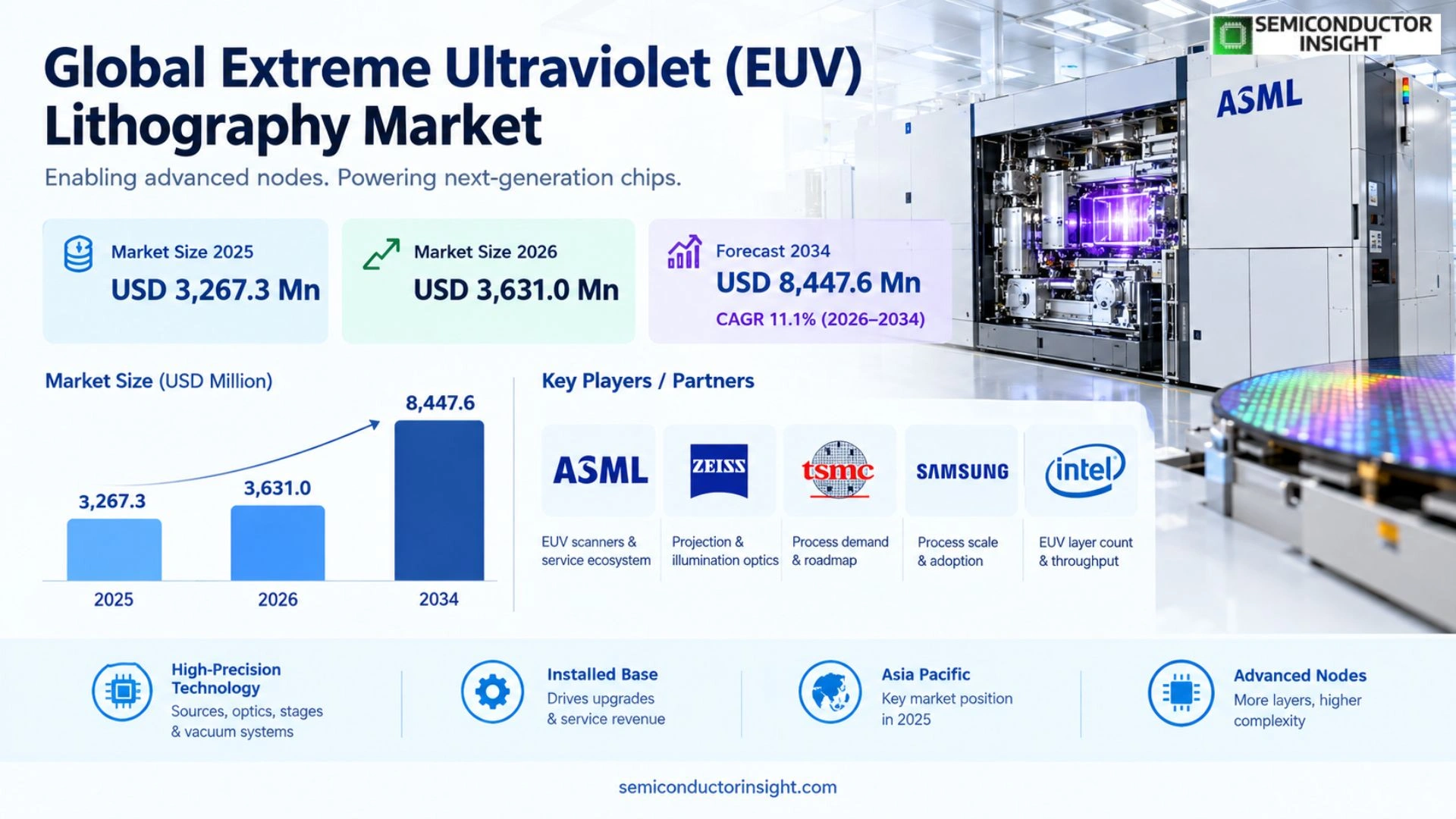
Global Extreme Ultraviolet (EUV) Lithography Market  Trends

Regional Analysis

Asia Pacific dominates EUV lithography demand with more than 75% share in the report scope, led by Taiwan and South Korea. North America is gaining strategic importance through Intel’s High-NA deployment and U.S. leading-edge fab investment, while Europe remains indispensable as the center of ASML and critical optical supply.

Why is the EUV market geographically concentrated?

Only a small number of companies operate leading-edge logic and memory fabs that can justify EUV’s cost and complexity. Taiwan and South Korea host large advanced foundry and memory capacity, the United States is expanding leading-edge production and High-NA qualification, and Europe supplies the scanners and optics even though local wafer demand is smaller.

Region Position Growth outlook Demand profile What decides supplier selection
Asia Pacific Largest >75% Very strong Leading-edge foundry and memory Node roadmap, EUV layer count and tool availability
North America High-NA production leader Strong Advanced logic, R&D and domestic fab expansion High-NA readiness, customer qualification and service
Europe Critical equipment & optics hub Strong strategic role Scanner, optics, research and selected fabs Technology leadership and supply-chain precision
South America Minimal direct market Limited Research and downstream semiconductor demand Capital intensity and absence of leading-edge fabs
Middle East & Africa Early-stage strategic market Long-term Research and future semiconductor diversification Fab economics, ecosystem and tool access
Asia Pacific LARGEST >75%

Why does Asia Pacific dominate EUV system demand?

Taiwan and South Korea operate some of the world’s largest leading-edge logic and memory fabs. EUV demand follows advanced wafer starts and the number of EUV layers per process node, so concentrated 3 nm, 2 nm and advanced DRAM production creates a large installed-base and upgrade market.

Market positionLargest region
Growth outlookVery strong
Demand profileFoundry and memory
Market access gateNode roadmap and tool capacity
Country / market Position in region Evidence-led demand logic
Taiwan Leading foundry market TSMC’s advanced-node manufacturing creates large EUV demand across successive logic generations.
South Korea Logic and memory hub Samsung and memory production create demand across advanced logic and DRAM EUV layers.
Japan Materials and equipment ecosystem Mask, resist, light-source and component suppliers support the broader EUV value chain.
China Limited leading-edge access Advanced-lithography restrictions constrain scanner deployment despite large semiconductor investment.

2026 – advanced logic and DRAM remain the main EUV growth engines

ASML’s 2026 roadmap positions NXE systems for 2 nm logic and advanced DRAM while High-NA prepares for later insertion.

Market relevance: EUV layer count and advanced wafer capacity drive both system demand and installed-base upgrades.

2026 – NXE:3800E productivity rises to 230 wafers per hour

ASML released a productivity enhancement package that lifts throughput while maintaining overlay performance.

Market relevance: Higher throughput increases effective EUV capacity without requiring one-for-one new scanner additions.

2025–2026 – High-NA systems operate at multiple customers

ASML reported eight High-NA systems shipped by the end of 2025, with several in operation.

Market relevance: Broader customer exposure accelerates process, mask and resist learning before full production insertion.

Full-report coverage: Detailed sub-market, geography, supplier and forecast analysis is retained in the full study; this overview focuses on the geographies with the clearest supportable demand mechanisms.
North America HIGH-NA PRODUCTION LEADER

Why is North America becoming more important in EUV lithography?

Intel has moved High-NA EUV from early qualification into selected production use on Intel 18A, while U.S. fab investment increases demand for advanced lithography support. The region also contains major semiconductor R&D, metrology and process-equipment ecosystems.

Market positionHigh-NA production leader
Growth outlookStrong
Demand profileAdvanced logic and R&D
Market access gateHigh-NA readiness and fab ramps
Country / market Position in region Evidence-led demand logic
United States Primary regional market Intel’s leading-edge manufacturing and new fab programs create direct EUV and High-NA demand.
Canada Research niche University and photonics research provide limited supporting demand rather than production-scale EUV deployment.
Mexico No major leading-edge EUV fabs Semiconductor activity is concentrated downstream in assembly and electronics manufacturing.

7 Sep 2026 – Intel and ASML report more than one million High-NA wafers processed

Intel Foundry and ASML stated that High-NA has been used across certification, R&D and volume production on selected Panther Lake layers.

Market relevance: The milestone demonstrates production readiness beyond small R&D lots.

15 Jul 2026 – High-NA enters high-volume logic production

ASML reported Intel Foundry using EXE High-NA technology on selected Intel 18A product layers with yields matching NXE-patterned layers.

Market relevance: Commercial High-NA adoption shifts the market from qualification toward production capacity.

16 Jun 2026 – Intel 18A-P enters risk production

Intel reported continued progress on its advanced process roadmap and leading-edge manufacturing.

Market relevance: Advanced process ramps sustain demand for EUV capacity and future High-NA insertion.

Full-report coverage: Detailed sub-market, geography, supplier and forecast analysis is retained in the full study; this overview focuses on the geographies with the clearest supportable demand mechanisms.
Europe SCANNER & OPTICS TECHNOLOGY HUB

Why is Europe strategically indispensable to EUV?

ASML in the Netherlands is the sole supplier of production EUV scanners, while ZEISS in Germany provides projection optics. Belgium’s imec and other research partners support process integration, masks, resists and High-NA learning. Europe therefore captures critical technology value even with less leading-edge wafer volume than Asia.

Market positionCritical supply hub
Growth outlookStrong strategic role
Demand profileScanner, optics and R&D
Market access gatePrecision manufacturing and supplier coordination
Country / market Position in region Evidence-led demand logic
Netherlands EUV scanner center ASML develops and assembles NXE and EXE systems and coordinates the global lithography supply chain.
Germany Optics and laser technology hub ZEISS manufactures EUV projection optics and other suppliers support source and precision components.
Belgium Researchecosystem imec supports advanced EUV and High-NA patterning research and ecosystem qualification.
Ireland Advanced logic manufacturing Intel’s EUV-enabled production expands regional wafer demand.

15 Apr 2026 – ASML presents 2026 EUV roadmap

The roadmap includes NXE:3800F and future NXE:4200 systems plus multiple High-NA EXE generations.

Market relevance: Long-term product cadence supports a sustained scanner replacement and upgrade cycle.

2026 – EXE:5200B reaches customer specifications

ASML states that its second-generation High-NA system combines improved overlay with higher productivity.

Market relevance: Production-oriented High-NA tools expand the addressable equipment value per advanced fab.

2025–2026 – ZEISS High-NA optics support sub-10 nm imaging

ZEISS describes 0.55 NA optical systems as enabling substantially finer imaging than current 0.33 NA EUV.

Market relevance: Optics precision remains one of the highest-barrier elements of the EUV supply chain.

Full-report coverage: Detailed sub-market, geography, supplier and forecast analysis is retained in the full study; this overview focuses on the geographies with the clearest supportable demand mechanisms.
South America MINIMAL DIRECT MARKET

Why is direct EUV demand limited in South America?

The region does not currently host leading-edge logic or memory fabs that justify production EUV tools. Semiconductor activity is concentrated in design, packaging, research and downstream electronics, so EUV exposure is indirect through imported advanced chips.

Market positionMinimal direct market
Growth outlookLimited
Demand profileResearch and downstream demand
Market access gateFab scale and capital intensity
Country / market Position in region Evidence-led demand logic
Brazil Largest semiconductor-policy market Research and packaging activity do not yet create production-scale EUV tool demand.
Argentina Research niche Academic semiconductor work creates indirect technology interest rather than commercial scanner demand.
Other South America Downstream users Advanced chips are imported, so EUV value is embedded upstream in foreign wafer fabs.

2025–2026 – semiconductor policy focuses below leading-edge EUV scale

Regional initiatives emphasize design, packaging and selected manufacturing.

Market relevance: The capital and ecosystem threshold for EUV remains far above current front-end capacity.

2026 – advanced chips enter through imported devices and servers

AI and electronics demand increases consumption of EUV-manufactured chips without local EUV equipment purchases.

Market relevance: Regional market exposure is therefore downstream rather than tool based.

Long-term – research partnerships can build lithography skills

Universities and international partnerships can develop patterning expertise before local leading-edge fabs emerge.

Market relevance: Near-term commercial scanner demand remains low.

Full-report coverage: Detailed sub-market, geography, supplier and forecast analysis is retained in the full study; this overview focuses on the geographies with the clearest supportable demand mechanisms.
Middle East & Africa EARLY-STAGE STRATEGIC MARKET

What could create future EUV demand in the Middle East and Africa?

The region is investing heavily in AI and advanced technology, but leading-edge wafer fabrication remains limited. EUV demand would require a full advanced-fab ecosystem, including masks, chemicals, metrology, cleanroom infrastructure and specialist workforce, making it a long-term rather than near-term market.

Market positionEarly-stage market
Growth outlookLong-term
Demand profileAdvanced-technology diversification
Market access gateFab ecosystem and capital
Country / market Position in region Evidence-led demand logic
Israel Semiconductor R&D and manufacturing niche Existing chip design and manufacturing expertise provides the strongest regional technical base.
United Arab Emirates Advanced-technology investment market AI and industrial diversification could support future semiconductor partnerships.
Saudi Arabia Long-term manufacturing opportunity Technology and industrial policy may create future front-end projects if economics and ecosystem mature.

2025–2026 – AI investment accelerates

Gulf states continue building large-scale compute infrastructure.

Market relevance: Demand for advanced chips rises, though lithography remains upstream in overseas fabs.

2026 – semiconductor diversification remains a policy topic

Regional technology strategies increasingly include advanced manufacturing.

Market relevance: Any future leading-edge fab would require EUV access and a global supplier ecosystem.

Long-term – workforce and supply-chain depth are prerequisites

EUV requires thousands of precision components and specialized service capability.

Market relevance: Tool demand will follow only after a sustainable advanced-fab base is established.

Full-report coverage: Detailed sub-market, geography, supplier and forecast analysis is retained in the full study; this overview focuses on the geographies with the clearest supportable demand mechanisms.

Competitive Landscape

ASML Holding is the dominant EUV scanner supplier, while Samsung Electronics, Intel and TSMC are major users and process developers. The wider ecosystem includes ZEISS optics, Ushio source components, Toppan Photomasks, NTT Advanced Technology, Nikon and Canon in adjacent lithography, mask and optical technologies.

ASML’s competitive position is unique because production EUV scanners require integration of high-power 13.5 nm sources, ultra-precise stages, vacuum systems, metrology and reflective optics. The installed base also creates substantial upgrade and service revenue.

ZEISS is a critical strategic partner through projection and illumination optics. The optical tolerances are so demanding that the scanner ecosystem cannot be replicated simply by assembling conventional semiconductor equipment components.

TSMC, Samsung and Intel influence the roadmap through process requirements and tool qualification. Their decisions on EUV layer count, High-NA insertion and throughput targets directly affect system demand and the broader mask, resist and metrology ecosystem.

Competitive tier Representative companies Commercial basis
EUV scanner leader ASML Holding NV Production NXE and EXE EUV systems, installed-base upgrades, service and system roadmap.
Critical ecosystem suppliers ZEISS; Ushio; Toppan Photomasks; NTT Advanced Technology Projection optics, source components, masks, coatings and supporting EUV infrastructure.
Leading-edge device manufacturers TSMC; Samsung Electronics; Intel High-volume EUV users that drive layer count, High-NA qualification and production requirements.

Key Participants

ASML Holding NV, Samsung Electronics, Canon Inc., Toppan Photomasks Inc., Ushio, Inc., NTT Advanced Technology Corporation, Nikon Corporation, Intel Corporation, Taiwan Semiconductor Manufacturing Company Limited.

Production Capacity Analysis

EUV production capacity is constrained by the rate at which ASML and its strategic suppliers can manufacture, integrate, ship and service scanners plus the ability of fabs to install cleanroom, utilities, masks and process infrastructure around each tool.

An EUV scanner integrates tens of thousands of precision components and subsystems. Long-lead optics, source modules, vacuum hardware, mechatronics and metrology must arrive in sequence for final assembly and customer shipment.

Installed-base productivity upgrades are effectively another form of capacity expansion. Raising throughput from 220 to 230 wafers per hour increases wafer exposure capacity without adding floor space for another scanner.

High-NA systems add more complex optics and a smaller exposure field, requiring stitching or product floor-planning for some designs. Fabs therefore need process, mask and EDA readiness in addition to the scanner itself.

Capacity layer Where it concentrates Commercial constraint
EUV scanner integration Netherlands / ASML supply network Long-lead precision subsystems, integration time and supplier capacity.
Projection optics Germany / ZEISS Mirror precision, coating quality and High-NA optical complexity.
Masks, pellicles & resists Japan, United States, Europe and Asia Defectivity, sensitivity, inspection and materials readiness.
Fab installation & service Taiwan, South Korea, United States, Europe and other advanced fabs Cleanroom utilities, uptime, field service and process qualification.

Market Dynamics

Growth is driven by advanced logic, AI and DRAM scaling, while the main restraints are extreme capital cost, concentrated supply, resist/mask challenges and the complexity of qualifying High-NA in production.

Market Drivers

Factor Directional impact Why it matters
2 nm and sub-2 nm logic High Advanced nodes require finer critical-layer patterning and higher lithography intensity.
Leading-edge DRAM High More DRAM layers are shifting toward EUV as pattern complexity increases.
High-NA transition High 0.55 NA can reduce multi-patterning and enable smaller single-exposure features.
AI semiconductor investment Medium-High AI accelerators drive advanced-node wafer demand and new leading-edge capacity.

Advanced logic needs simpler patterning

EUV can replace several DUV multi-patterning steps with one exposure, reducing overlay accumulation, cycle time and process complexity on suitable layers.

DRAM is becoming more EUV intensive

ASML has highlighted increased EUV use in newer DRAM generations, adding scanner demand beyond logic foundries.

High-NA creates a new equipment generation

EXE systems raise numerical aperture and imaging contrast, giving fabs another scaling option when 0.33 NA requires complex multi-patterning.

AI demand supports leading-edge wafer starts

Accelerators and high-performance CPUs are disproportionately manufactured at advanced nodes, supporting EUV utilization and fab investment.

Market Restraints

Factor Directional impact Why it matters
Extreme capital cost High Each EUV system represents very large equipment and facility investment.
Single-supplier concentration High ASML is the sole production EUV scanner supplier.
Mask / resist complexity High EUV requires specialized reflective masks, pellicles, resists and inspection.
High-NA half-field challenge Medium-High 0.55 NA changes field size and can require stitching or design adjustments.

Capital intensity limits the customer base

Only high-volume leading-edge fabs can justify EUV tool cost, cleanroom space and supporting infrastructure.

Supply concentration creates strategic risk

A bottleneck in scanners, optics or key subsystems can directly constrain global advanced-node capacity.

Materials must improve with resolution

Higher sensitivity can increase stochastic defects and roughness, so resist and mask ecosystems must advance alongside scanner optics.

High-NA changes design and mask flows

The smaller field and tighter process window require new EDA, stitching, mask and overlay approaches before broad insertion.

Market Opportunities

High-NA production insertion

EXE tools can shift selected future critical layers from multi-patterning to single exposure.

Installed-base productivity upgrades

Higher wafers per hour can monetize existing fab floor space and reduce cost per exposure.

Advanced DRAM EUV layers

Memory scaling can add EUV demand even when logic-node transitions slow.

Mask, resist and metrology ecosystem

Every High-NA insertion creates new demand for supporting materials, inspection and computational lithography.

Supply Chain Analysis

EUV Source & Optics
13.5 nm light and multilayer mirrors create the imaging system.
Scanner Integration
ASML combines source, stages, optics, vacuum and metrology into NXE/EXE systems.
Masks, Resists & Process
Fabs qualify reflective masks, photoresists, pellicles and patterning recipes.
High-Volume Manufacturing
Foundries, IDMs and memory fabs expose production wafers and continuously optimize throughput.

EUV Source & Optics. High-power source stability and projection-mirror precision are fundamental to throughput and resolution. These components have very high technical barriers.

Scanner Integration. System assembly requires synchronization of optics, stages, vacuum, metrology and contamination control at nanometer and sub-nanometer precision.

Masks, Resists & Process. EUV materials must balance sensitivity, roughness and defectivity. High-NA creates tighter requirements and new mask-field considerations.

High-Volume Manufacturing. Fab economics depend on utilization, wafers per hour, uptime and the number of process steps eliminated relative to alternative patterning flows.

Recent Developments in the Extreme Ultraviolet (EUV) Lithography Market

Developments tracked to September 2026. Entries use official publication dates where available.

  • 7 September 2026High-NA scale
    Intel Foundry and ASML reported more than one million wafers processed using High-NA systems across certification, R&D and selected volume-production layers. Overlay, throughput and availability were reported to be meeting Intel’s expectations.

    Source

  • 15 July 2026Production milestone
    ASML reported that Intel Foundry entered high-volume manufacturing using EXE High-NA EUV on selected Intel 18A product layers. Yields on those layers matched the NXE platform.

    Source

  • 15 April 2026Productivity
    ASML released a productivity enhancement for NXE:3800E, raising throughput from 220 to 230 wafers per hour at similar overlay. The upgrade increases effective EUV capacity in high-volume fabs.

    Source

  • 28 January 2026High-NA fleet
    ASML reported eight High-NA systems shipped and six operating at customer sites, including the first second-generation EXE:5200B meeting full specifications.

    Source

  • 2026System roadmap
    ASML’s EXE:5200B combines 0.55 NA optics, 8 nm resolution and higher productivity for future high-volume manufacturing. The platform is designed to reduce process complexity as High-NA moves into advanced nodes.

    Source

Report Scope & Segmentation

Attribute Coverage
Report title Global Extreme Ultraviolet (EUV) Lithography Market Research Report 2025(Status and Outlook)
Base Year 2025
Estimated Year 2026
Forecast Period 2026–2034
By Type Light Source; Mask; Mirrors; Others
By Application Foundry; Integrated Device Manufacturers (IDM); Memory; Others
By Node Size 5nm and below; 7nm; 10nm; Others
Regions North America; Europe; Asia Pacific; South America; Middle East & Africa
Companies ASML Holding NV; Samsung Electronics; Canon Inc.; Toppan Photomasks Inc.; Ushio, Inc.; NTT Advanced Technology Corporation; Nikon Corporation; Intel Corporation; Taiwan Semiconductor Manufacturing Company Limited
Customization scope Country, segment, company, application, technology, production and competitive-detail customization available within the study scope.

Frequently Asked Questions

What is the size of the EUV Lithography market?

The global EUV Lithography market is valued at USD 3,267.3 million in 2025, is estimated at USD 3,631.0 million in 2026, and is projected to reach USD 8,447.6 million by 2034, representing a 11.1% CAGR during 2026–2034. This remains commercially relevant because technical qualification, security or reliability, lifecycle support and supply continuity can materially affect buyer selection across the 2026–2034 forecast period. This remains commercially relevant because technical qualification, security or reliability, lifecycle support and supply continuity can materially affect buyer selection across the 2026–2034 forecast period.

Which region leads EUV lithography?

Asia Pacific leads with more than 75% of demand in the report scope, supported by advanced foundry and memory manufacturing in Taiwan and South Korea. This remains commercially relevant because technical qualification, security or reliability, lifecycle support and supply continuity can materially affect buyer selection across the 2026–2034 forecast period. This remains commercially relevant because technical qualification, security or reliability, lifecycle support and supply continuity can materially affect buyer selection across the 2026–2034 forecast period.

Which type segment leads?

Light Source leads because source power, stability and dose control directly determine EUV scanner throughput and manufacturing productivity. This remains commercially relevant because technical qualification, security or reliability, lifecycle support and supply continuity can materially affect buyer selection across the 2026–2034 forecast period. This remains commercially relevant because technical qualification, security or reliability, lifecycle support and supply continuity can materially affect buyer selection across the 2026–2034 forecast period.

Which application leads?

Foundry is the leading application due to high-volume advanced logic manufacturing at 5 nm, 3 nm, 2 nm and future nodes. This remains commercially relevant because technical qualification, security or reliability, lifecycle support and supply continuity can materially affect buyer selection across the 2026–2034 forecast period. This remains commercially relevant because technical qualification, security or reliability, lifecycle support and supply continuity can materially affect buyer selection across the 2026–2034 forecast period.

What is High-NA EUV?

High-NA EUV raises numerical aperture from 0.33 to 0.55, improving resolution and imaging contrast so smaller features can be printed with less multi-patterning. This remains commercially relevant because technical qualification, security or reliability, lifecycle support and supply continuity can materially affect buyer selection across the 2026–2034 forecast period. This remains commercially relevant because technical qualification, security or reliability, lifecycle support and supply continuity can materially affect buyer selection across the 2026–2034 forecast period.

Why is EUV important for DRAM?

New DRAM generations use increasingly complex patterning, and more layers can move from DUV multi-patterning to EUV to reduce cycle time and overlay complexity. This remains commercially relevant because technical qualification, security or reliability, lifecycle support and supply continuity can materially affect buyer selection across the 2026–2034 forecast period. This remains commercially relevant because technical qualification, security or reliability, lifecycle support and supply continuity can materially affect buyer selection across the 2026–2034 forecast period.

What are the main restraints?

Extreme capital cost, reliance on a single scanner supplier, mask and resist complexity, and High-NA design-field challenges are the main restraints. This remains commercially relevant because technical qualification, security or reliability, lifecycle support and supply continuity can materially affect buyer selection across the 2026–2034 forecast period. This remains commercially relevant because technical qualification, security or reliability, lifecycle support and supply continuity can materially affect buyer selection across the 2026–2034 forecast period.

Who are the major companies?

Key participants include ASML, Samsung Electronics, Toppan Photomasks, Ushio, NTT Advanced Technology, Intel and TSMC, with ZEISS critical to EUV optics. This remains commercially relevant because technical qualification, security or reliability, lifecycle support and supply continuity can materially affect buyer selection across the 2026–2034 forecast period. This remains commercially relevant because technical qualification, security or reliability, lifecycle support and supply continuity can materially affect buyer selection across the 2026–2034 forecast period.

How does throughput affect market economics?

Higher wafers per hour increases effective fab capacity and lowers cost per exposure, so installed-base productivity upgrades can create value similar to adding new tool capacity. This remains commercially relevant because technical qualification, security or reliability, lifecycle support and supply continuity can materially affect buyer selection across the 2026–2034 forecast period. This remains commercially relevant because technical qualification, security or reliability, lifecycle support and supply continuity can materially affect buyer selection across the 2026–2034 forecast period.

Where are the strongest opportunities?

The strongest opportunities are in High-NA production insertion, installed-base productivity upgrades, advanced DRAM EUV layers and the mask/resist/metrology ecosystem. This remains commercially relevant because technical qualification, security or reliability, lifecycle support and supply continuity can materially affect buyer selection across the 2026–2034 forecast period. This remains commercially relevant because technical qualification, security or reliability, lifecycle support and supply continuity can materially affect buyer selection across the 2026–2034 forecast period.

Research Sources & Evidence Base

View research sources used for this overview
  1. ASML. High-NA EUV Production Milestone, 2026 Intel 18A High-NA production use..
  2. Intel Foundry. Intel and ASML High-NA Readiness, September 2026 High-NA wafer and production milestone..
  3. ASML. TWINSCAN EXE:5200B, 0.55 NA, 8 nm resolution and High-NA system capabilities..
  4. ASML. TWINSCAN NXE:3800E, 0.33 NA EUV system for 2 nm logic and leading-edge DRAM..
  5. ASML. Q1 2026 EUV Product Roadmap, NXE and EXE throughput and roadmap..
  6. ZEISS. Semiconductor Manufacturing Optics Overview, High-NA EUV optical systems and sub-10 nm imaging..
  7. Intel. High-NA EUV at Intel, First commercial High-NA installation and technology role..
Global Extreme Ultraviolet (EUV) Lithography Market Research Report 2026-2034

Get Sample Report PDF for Exclusive Insights

Report Sample Includes

  • Table of Contents
  • List of Tables & Figures
  • Charts, Research Methodology, and more...

PDF Icon Download Sample Report PDF
SKU: b8138fbb2e4f
Category:

Download Sample Report

Table of Content

Table of Contents
1 Research Methodology and Statistical Scope
1.1 Market Definition and Statistical Scope of Extreme Ultraviolet (EUV) Lithography
1.2 Key Market Segments
1.2.1 Extreme Ultraviolet (EUV) Lithography Segment by Type
1.2.2 Extreme Ultraviolet (EUV) Lithography Segment by Application
1.3 Methodology & Sources of Information
1.3.1 Research Methodology
1.3.2 Research Process
1.3.3 Market Breakdown and Data Triangulation
1.3.4 Base Year
1.3.5 Report Assumptions & Caveats
2 Extreme Ultraviolet (EUV) Lithography Market Overview
2.1 Global Market Overview
2.1.1 Global Extreme Ultraviolet (EUV) Lithography Market Size (M USD) Estimates and Forecasts (2019-2032)
2.1.2 Global Extreme Ultraviolet (EUV) Lithography Sales Estimates and Forecasts (2019-2032)
2.2 Market Segment Executive Summary
2.3 Global Market Size by Region
3 Extreme Ultraviolet (EUV) Lithography Market Competitive Landscape
3.1 Global Extreme Ultraviolet (EUV) Lithography Sales by Manufacturers (2019-2025)
3.2 Global Extreme Ultraviolet (EUV) Lithography Revenue Market Share by Manufacturers (2019-2025)
3.3 Extreme Ultraviolet (EUV) Lithography Market Share by Company Type (Tier 1, Tier 2, and Tier 3)
3.4 Global Extreme Ultraviolet (EUV) Lithography Average Price by Manufacturers (2019-2025)
3.5 Manufacturers Extreme Ultraviolet (EUV) Lithography Sales Sites, Area Served, Product Type
3.6 Extreme Ultraviolet (EUV) Lithography Market Competitive Situation and Trends
3.6.1 Extreme Ultraviolet (EUV) Lithography Market Concentration Rate
3.6.2 Global 5 and 10 Largest Extreme Ultraviolet (EUV) Lithography Players Market Share by Revenue
3.6.3 Mergers & Acquisitions, Expansion
4 Extreme Ultraviolet (EUV) Lithography Industry Chain Analysis
4.1 Extreme Ultraviolet (EUV) Lithography Industry Chain Analysis
4.2 Market Overview of Key Raw Materials
4.3 Midstream Market Analysis
4.4 Downstream Customer Analysis
5 The Development and Dynamics of Extreme Ultraviolet (EUV) Lithography Market
5.1 Key Development Trends
5.2 Driving Factors
5.3 Market Challenges
5.4 Market Restraints
5.5 Industry News
5.5.1 New Product Developments
5.5.2 Mergers & Acquisitions
5.5.3 Expansions
5.5.4 Collaboration/Supply Contracts
5.6 Industry Policies
6 Extreme Ultraviolet (EUV) Lithography Market Segmentation by Type
6.1 Evaluation Matrix of Segment Market Development Potential (Type)
6.2 Global Extreme Ultraviolet (EUV) Lithography Sales Market Share by Type (2019-2025)
6.3 Global Extreme Ultraviolet (EUV) Lithography Market Size Market Share by Type (2019-2025)
6.4 Global Extreme Ultraviolet (EUV) Lithography Price by Type (2019-2025)
7 Extreme Ultraviolet (EUV) Lithography Market Segmentation by Application
7.1 Evaluation Matrix of Segment Market Development Potential (Application)
7.2 Global Extreme Ultraviolet (EUV) Lithography Market Sales by Application (2019-2025)
7.3 Global Extreme Ultraviolet (EUV) Lithography Market Size (M USD) by Application (2019-2025)
7.4 Global Extreme Ultraviolet (EUV) Lithography Sales Growth Rate by Application (2019-2025)
8 Extreme Ultraviolet (EUV) Lithography Market Segmentation by Region
8.1 Global Extreme Ultraviolet (EUV) Lithography Sales by Region
8.1.1 Global Extreme Ultraviolet (EUV) Lithography Sales by Region
8.1.2 Global Extreme Ultraviolet (EUV) Lithography Sales Market Share by Region
8.2 North America
8.2.1 North America Extreme Ultraviolet (EUV) Lithography Sales by Country
8.2.2 U.S.
8.2.3 Canada
8.2.4 Mexico
8.3 Europe
8.3.1 Europe Extreme Ultraviolet (EUV) Lithography Sales by Country
8.3.2 Germany
8.3.3 France
8.3.4 U.K.
8.3.5 Italy
8.3.6 Russia
8.4 Asia Pacific
8.4.1 Asia Pacific Extreme Ultraviolet (EUV) Lithography Sales by Region
8.4.2 China
8.4.3 Japan
8.4.4 South Korea
8.4.5 India
8.4.6 Southeast Asia
8.5 South America
8.5.1 South America Extreme Ultraviolet (EUV) Lithography Sales by Country
8.5.2 Brazil
8.5.3 Argentina
8.5.4 Columbia
8.6 Middle East and Africa
8.6.1 Middle East and Africa Extreme Ultraviolet (EUV) Lithography Sales by Region
8.6.2 Saudi Arabia
8.6.3 UAE
8.6.4 Egypt
8.6.5 Nigeria
8.6.6 South Africa
9 Key Companies Profile
9.1 Canon Inc
9.1.1 Canon Inc Extreme Ultraviolet (EUV) Lithography Basic Information
9.1.2 Canon Inc Extreme Ultraviolet (EUV) Lithography Product Overview
9.1.3 Canon Inc Extreme Ultraviolet (EUV) Lithography Product Market Performance
9.1.4 Canon Inc Business Overview
9.1.5 Canon Inc Extreme Ultraviolet (EUV) Lithography SWOT Analysis
9.1.6 Canon Inc Recent Developments
9.2 Samsung Electronics
9.2.1 Samsung Electronics Extreme Ultraviolet (EUV) Lithography Basic Information
9.2.2 Samsung Electronics Extreme Ultraviolet (EUV) Lithography Product Overview
9.2.3 Samsung Electronics Extreme Ultraviolet (EUV) Lithography Product Market Performance
9.2.4 Samsung Electronics Business Overview
9.2.5 Samsung Electronics Extreme Ultraviolet (EUV) Lithography SWOT Analysis
9.2.6 Samsung Electronics Recent Developments
9.3 Toppan Photomasks Inc.
9.3.1 Toppan Photomasks Inc. Extreme Ultraviolet (EUV) Lithography Basic Information
9.3.2 Toppan Photomasks Inc. Extreme Ultraviolet (EUV) Lithography Product Overview
9.3.3 Toppan Photomasks Inc. Extreme Ultraviolet (EUV) Lithography Product Market Performance
9.3.4 Toppan Photomasks Inc. Extreme Ultraviolet (EUV) Lithography SWOT Analysis
9.3.5 Toppan Photomasks Inc. Business Overview
9.3.6 Toppan Photomasks Inc. Recent Developments
9.4 Ushio, Inc.
9.4.1 Ushio, Inc. Extreme Ultraviolet (EUV) Lithography Basic Information
9.4.2 Ushio, Inc. Extreme Ultraviolet (EUV) Lithography Product Overview
9.4.3 Ushio, Inc. Extreme Ultraviolet (EUV) Lithography Product Market Performance
9.4.4 Ushio, Inc. Business Overview
9.4.5 Ushio, Inc. Recent Developments
9.5 ASML Holding NV
9.5.1 ASML Holding NV Extreme Ultraviolet (EUV) Lithography Basic Information
9.5.2 ASML Holding NV Extreme Ultraviolet (EUV) Lithography Product Overview
9.5.3 ASML Holding NV Extreme Ultraviolet (EUV) Lithography Product Market Performance
9.5.4 ASML Holding NV Business Overview
9.5.5 ASML Holding NV Recent Developments
9.6 NTT Advanced Technology Corporation
9.6.1 NTT Advanced Technology Corporation Extreme Ultraviolet (EUV) Lithography Basic Information
9.6.2 NTT Advanced Technology Corporation Extreme Ultraviolet (EUV) Lithography Product Overview
9.6.3 NTT Advanced Technology Corporation Extreme Ultraviolet (EUV) Lithography Product Market Performance
9.6.4 NTT Advanced Technology Corporation Business Overview
9.6.5 NTT Advanced Technology Corporation Recent Developments
9.7 Nikon Corporation
9.7.1 Nikon Corporation Extreme Ultraviolet (EUV) Lithography Basic Information
9.7.2 Nikon Corporation Extreme Ultraviolet (EUV) Lithography Product Overview
9.7.3 Nikon Corporation Extreme Ultraviolet (EUV) Lithography Product Market Performance
9.7.4 Nikon Corporation Business Overview
9.7.5 Nikon Corporation Recent Developments
9.8 Intel Corporation
9.8.1 Intel Corporation Extreme Ultraviolet (EUV) Lithography Basic Information
9.8.2 Intel Corporation Extreme Ultraviolet (EUV) Lithography Product Overview
9.8.3 Intel Corporation Extreme Ultraviolet (EUV) Lithography Product Market Performance
9.8.4 Intel Corporation Business Overview
9.8.5 Intel Corporation Recent Developments
9.9 Taiwan Semiconductor Manufacturing Company Limited
9.9.1 Taiwan Semiconductor Manufacturing Company Limited Extreme Ultraviolet (EUV) Lithography Basic Information
9.9.2 Taiwan Semiconductor Manufacturing Company Limited Extreme Ultraviolet (EUV) Lithography Product Overview
9.9.3 Taiwan Semiconductor Manufacturing Company Limited Extreme Ultraviolet (EUV) Lithography Product Market Performance
9.9.4 Taiwan Semiconductor Manufacturing Company Limited Business Overview
9.9.5 Taiwan Semiconductor Manufacturing Company Limited Recent Developments
10 Extreme Ultraviolet (EUV) Lithography Market Forecast by Region
10.1 Global Extreme Ultraviolet (EUV) Lithography Market Size Forecast
10.2 Global Extreme Ultraviolet (EUV) Lithography Market Forecast by Region
10.2.1 North America Market Size Forecast by Country
10.2.2 Europe Extreme Ultraviolet (EUV) Lithography Market Size Forecast by Country
10.2.3 Asia Pacific Extreme Ultraviolet (EUV) Lithography Market Size Forecast by Region
10.2.4 South America Extreme Ultraviolet (EUV) Lithography Market Size Forecast by Country
10.2.5 Middle East and Africa Forecasted Consumption of Extreme Ultraviolet (EUV) Lithography by Country
11 Forecast Market by Type and by Application (2025-2032)
11.1 Global Extreme Ultraviolet (EUV) Lithography Market Forecast by Type (2025-2032)
11.1.1 Global Forecasted Sales of Extreme Ultraviolet (EUV) Lithography by Type (2025-2032)
11.1.2 Global Extreme Ultraviolet (EUV) Lithography Market Size Forecast by Type (2025-2032)
11.1.3 Global Forecasted Price of Extreme Ultraviolet (EUV) Lithography by Type (2025-2032)
11.2 Global Extreme Ultraviolet (EUV) Lithography Market Forecast by Application (2025-2032)
11.2.1 Global Extreme Ultraviolet (EUV) Lithography Sales (K Units) Forecast by Application
11.2.2 Global Extreme Ultraviolet (EUV) Lithography Market Size (M USD) Forecast by Application (2025-2032)
12 Conclusion and Key FindingsList of Tables
Table 1. Introduction of the Type
Table 2. Introduction of the Application
Table 3. Market Size (M USD) Segment Executive Summary
Table 4. Extreme Ultraviolet (EUV) Lithography Market Size Comparison by Region (M USD)
Table 5. Global Extreme Ultraviolet (EUV) Lithography Sales (K Units) by Manufacturers (2019-2025)
Table 6. Global Extreme Ultraviolet (EUV) Lithography Sales Market Share by Manufacturers (2019-2025)
Table 7. Global Extreme Ultraviolet (EUV) Lithography Revenue (M USD) by Manufacturers (2019-2025)
Table 8. Global Extreme Ultraviolet (EUV) Lithography Revenue Share by Manufacturers (2019-2025)
Table 9. Company Type (Tier 1, Tier 2, and Tier 3) & (based on the Revenue in Extreme Ultraviolet (EUV) Lithography as of 2022)
Table 10. Global Market Extreme Ultraviolet (EUV) Lithography Average Price (USD/Unit) of Key Manufacturers (2019-2025)
Table 11. Manufacturers Extreme Ultraviolet (EUV) Lithography Sales Sites and Area Served
Table 12. Manufacturers Extreme Ultraviolet (EUV) Lithography Product Type
Table 13. Global Extreme Ultraviolet (EUV) Lithography Manufacturers Market Concentration Ratio (CR5 and HHI)
Table 14. Mergers & Acquisitions, Expansion Plans
Table 15. Industry Chain Map of Extreme Ultraviolet (EUV) Lithography
Table 16. Market Overview of Key Raw Materials
Table 17. Midstream Market Analysis
Table 18. Downstream Customer Analysis
Table 19. Key Development Trends
Table 20. Driving Factors
Table 21. Extreme Ultraviolet (EUV) Lithography Market Challenges
Table 22. Global Extreme Ultraviolet (EUV) Lithography Sales by Type (K Units)
Table 23. Global Extreme Ultraviolet (EUV) Lithography Market Size by Type (M USD)
Table 24. Global Extreme Ultraviolet (EUV) Lithography Sales (K Units) by Type (2019-2025)
Table 25. Global Extreme Ultraviolet (EUV) Lithography Sales Market Share by Type (2019-2025)
Table 26. Global Extreme Ultraviolet (EUV) Lithography Market Size (M USD) by Type (2019-2025)
Table 27. Global Extreme Ultraviolet (EUV) Lithography Market Size Share by Type (2019-2025)
Table 28. Global Extreme Ultraviolet (EUV) Lithography Price (USD/Unit) by Type (2019-2025)
Table 29. Global Extreme Ultraviolet (EUV) Lithography Sales (K Units) by Application
Table 30. Global Extreme Ultraviolet (EUV) Lithography Market Size by Application
Table 31. Global Extreme Ultraviolet (EUV) Lithography Sales by Application (2019-2025) & (K Units)
Table 32. Global Extreme Ultraviolet (EUV) Lithography Sales Market Share by Application (2019-2025)
Table 33. Global Extreme Ultraviolet (EUV) Lithography Sales by Application (2019-2025) & (M USD)
Table 34. Global Extreme Ultraviolet (EUV) Lithography Market Share by Application (2019-2025)
Table 35. Global Extreme Ultraviolet (EUV) Lithography Sales Growth Rate by Application (2019-2025)
Table 36. Global Extreme Ultraviolet (EUV) Lithography Sales by Region (2019-2025) & (K Units)
Table 37. Global Extreme Ultraviolet (EUV) Lithography Sales Market Share by Region (2019-2025)
Table 38. North America Extreme Ultraviolet (EUV) Lithography Sales by Country (2019-2025) & (K Units)
Table 39. Europe Extreme Ultraviolet (EUV) Lithography Sales by Country (2019-2025) & (K Units)
Table 40. Asia Pacific Extreme Ultraviolet (EUV) Lithography Sales by Region (2019-2025) & (K Units)
Table 41. South America Extreme Ultraviolet (EUV) Lithography Sales by Country (2019-2025) & (K Units)
Table 42. Middle East and Africa Extreme Ultraviolet (EUV) Lithography Sales by Region (2019-2025) & (K Units)
Table 43. Canon Inc Extreme Ultraviolet (EUV) Lithography Basic Information
Table 44. Canon Inc Extreme Ultraviolet (EUV) Lithography Product Overview
Table 45. Canon Inc Extreme Ultraviolet (EUV) Lithography Sales (K Units), Revenue (M USD), Price (USD/Unit) and Gross Margin (2019-2025)
Table 46. Canon Inc Business Overview
Table 47. Canon Inc Extreme Ultraviolet (EUV) Lithography SWOT Analysis
Table 48. Canon Inc Recent Developments
Table 49. Samsung Electronics Extreme Ultraviolet (EUV) Lithography Basic Information
Table 50. Samsung Electronics Extreme Ultraviolet (EUV) Lithography Product Overview
Table 51. Samsung Electronics Extreme Ultraviolet (EUV) Lithography Sales (K Units), Revenue (M USD), Price (USD/Unit) and Gross Margin (2019-2025)
Table 52. Samsung Electronics Business Overview
Table 53. Samsung Electronics Extreme Ultraviolet (EUV) Lithography SWOT Analysis
Table 54. Samsung Electronics Recent Developments
Table 55. Toppan Photomasks Inc. Extreme Ultraviolet (EUV) Lithography Basic Information
Table 56. Toppan Photomasks Inc. Extreme Ultraviolet (EUV) Lithography Product Overview
Table 57. Toppan Photomasks Inc. Extreme Ultraviolet (EUV) Lithography Sales (K Units), Revenue (M USD), Price (USD/Unit) and Gross Margin (2019-2025)
Table 58. Toppan Photomasks Inc. Extreme Ultraviolet (EUV) Lithography SWOT Analysis
Table 59. Toppan Photomasks Inc. Business Overview
Table 60. Toppan Photomasks Inc. Recent Developments
Table 61. Ushio, Inc. Extreme Ultraviolet (EUV) Lithography Basic Information
Table 62. Ushio, Inc. Extreme Ultraviolet (EUV) Lithography Product Overview
Table 63. Ushio, Inc. Extreme Ultraviolet (EUV) Lithography Sales (K Units), Revenue (M USD), Price (USD/Unit) and Gross Margin (2019-2025)
Table 64. Ushio, Inc. Business Overview
Table 65. Ushio, Inc. Recent Developments
Table 66. ASML Holding NV Extreme Ultraviolet (EUV) Lithography Basic Information
Table 67. ASML Holding NV Extreme Ultraviolet (EUV) Lithography Product Overview
Table 68. ASML Holding NV Extreme Ultraviolet (EUV) Lithography Sales (K Units), Revenue (M USD), Price (USD/Unit) and Gross Margin (2019-2025)
Table 69. ASML Holding NV Business Overview
Table 70. ASML Holding NV Recent Developments
Table 71. NTT Advanced Technology Corporation Extreme Ultraviolet (EUV) Lithography Basic Information
Table 72. NTT Advanced Technology Corporation Extreme Ultraviolet (EUV) Lithography Product Overview
Table 73. NTT Advanced Technology Corporation Extreme Ultraviolet (EUV) Lithography Sales (K Units), Revenue (M USD), Price (USD/Unit) and Gross Margin (2019-2025)
Table 74. NTT Advanced Technology Corporation Business Overview
Table 75. NTT Advanced Technology Corporation Recent Developments
Table 76. Nikon Corporation Extreme Ultraviolet (EUV) Lithography Basic Information
Table 77. Nikon Corporation Extreme Ultraviolet (EUV) Lithography Product Overview
Table 78. Nikon Corporation Extreme Ultraviolet (EUV) Lithography Sales (K Units), Revenue (M USD), Price (USD/Unit) and Gross Margin (2019-2025)
Table 79. Nikon Corporation Business Overview
Table 80. Nikon Corporation Recent Developments
Table 81. Intel Corporation Extreme Ultraviolet (EUV) Lithography Basic Information
Table 82. Intel Corporation Extreme Ultraviolet (EUV) Lithography Product Overview
Table 83. Intel Corporation Extreme Ultraviolet (EUV) Lithography Sales (K Units), Revenue (M USD), Price (USD/Unit) and Gross Margin (2019-2025)
Table 84. Intel Corporation Business Overview
Table 85. Intel Corporation Recent Developments
Table 86. Taiwan Semiconductor Manufacturing Company Limited Extreme Ultraviolet (EUV) Lithography Basic Information
Table 87. Taiwan Semiconductor Manufacturing Company Limited Extreme Ultraviolet (EUV) Lithography Product Overview
Table 88. Taiwan Semiconductor Manufacturing Company Limited Extreme Ultraviolet (EUV) Lithography Sales (K Units), Revenue (M USD), Price (USD/Unit) and Gross Margin (2019-2025)
Table 89. Taiwan Semiconductor Manufacturing Company Limited Business Overview
Table 90. Taiwan Semiconductor Manufacturing Company Limited Recent Developments
Table 91. Global Extreme Ultraviolet (EUV) Lithography Sales Forecast by Region (2025-2032) & (K Units)
Table 92. Global Extreme Ultraviolet (EUV) Lithography Market Size Forecast by Region (2025-2032) & (M USD)
Table 93. North America Extreme Ultraviolet (EUV) Lithography Sales Forecast by Country (2025-2032) & (K Units)
Table 94. North America Extreme Ultraviolet (EUV) Lithography Market Size Forecast by Country (2025-2032) & (M USD)
Table 95. Europe Extreme Ultraviolet (EUV) Lithography Sales Forecast by Country (2025-2032) & (K Units)
Table 96. Europe Extreme Ultraviolet (EUV) Lithography Market Size Forecast by Country (2025-2032) & (M USD)
Table 97. Asia Pacific Extreme Ultraviolet (EUV) Lithography Sales Forecast by Region (2025-2032) & (K Units)
Table 98. Asia Pacific Extreme Ultraviolet (EUV) Lithography Market Size Forecast by Region (2025-2032) & (M USD)
Table 99. South America Extreme Ultraviolet (EUV) Lithography Sales Forecast by Country (2025-2032) & (K Units)
Table 100. South America Extreme Ultraviolet (EUV) Lithography Market Size Forecast by Country (2025-2032) & (M USD)
Table 101. Middle East and Africa Extreme Ultraviolet (EUV) Lithography Consumption Forecast by Country (2025-2032) & (Units)
Table 102. Middle East and Africa Extreme Ultraviolet (EUV) Lithography Market Size Forecast by Country (2025-2032) & (M USD)
Table 103. Global Extreme Ultraviolet (EUV) Lithography Sales Forecast by Type (2025-2032) & (K Units)
Table 104. Global Extreme Ultraviolet (EUV) Lithography Market Size Forecast by Type (2025-2032) & (M USD)
Table 105. Global Extreme Ultraviolet (EUV) Lithography Price Forecast by Type (2025-2032) & (USD/Unit)
Table 106. Global Extreme Ultraviolet (EUV) Lithography Sales (K Units) Forecast by Application (2025-2032)
Table 107. Global Extreme Ultraviolet (EUV) Lithography Market Size Forecast by Application (2025-2032) & (M USD)
List of Figures
Figure 1. Product Picture of Extreme Ultraviolet (EUV) Lithography
Figure 2. Data Triangulation
Figure 3. Key Caveats
Figure 4. Global Extreme Ultraviolet (EUV) Lithography Market Size (M USD), 2019-2032
Figure 5. Global Extreme Ultraviolet (EUV) Lithography Market Size (M USD) (2019-2032)
Figure 6. Global Extreme Ultraviolet (EUV) Lithography Sales (K Units) & (2019-2032)
Figure 7. Evaluation Matrix of Segment Market Development Potential (Type)
Figure 8. Evaluation Matrix of Segment Market Development Potential (Application)
Figure 9. Evaluation Matrix of Regional Market Development Potential
Figure 10. Extreme Ultraviolet (EUV) Lithography Market Size by Country (M USD)
Figure 11. Extreme Ultraviolet (EUV) Lithography Sales Share by Manufacturers in 2023
Figure 12. Global Extreme Ultraviolet (EUV) Lithography Revenue Share by Manufacturers in 2023
Figure 13. Extreme Ultraviolet (EUV) Lithography Market Share by Company Type (Tier 1, Tier 2 and Tier 3): 2023
Figure 14. Global Market Extreme Ultraviolet (EUV) Lithography Average Price (USD/Unit) of Key Manufacturers in 2023
Figure 15. The Global 5 and 10 Largest Players: Market Share by Extreme Ultraviolet (EUV) Lithography Revenue in 2023
Figure 16. Evaluation Matrix of Segment Market Development Potential (Type)
Figure 17. Global Extreme Ultraviolet (EUV) Lithography Market Share by Type
Figure 18. Sales Market Share of Extreme Ultraviolet (EUV) Lithography by Type (2019-2025)
Figure 19. Sales Market Share of Extreme Ultraviolet (EUV) Lithography by Type in 2023
Figure 20. Market Size Share of Extreme Ultraviolet (EUV) Lithography by Type (2019-2025)
Figure 21. Market Size Market Share of Extreme Ultraviolet (EUV) Lithography by Type in 2023
Figure 22. Evaluation Matrix of Segment Market Development Potential (Application)
Figure 23. Global Extreme Ultraviolet (EUV) Lithography Market Share by Application
Figure 24. Global Extreme Ultraviolet (EUV) Lithography Sales Market Share by Application (2019-2025)
Figure 25. Global Extreme Ultraviolet (EUV) Lithography Sales Market Share by Application in 2023
Figure 26. Global Extreme Ultraviolet (EUV) Lithography Market Share by Application (2019-2025)
Figure 27. Global Extreme Ultraviolet (EUV) Lithography Market Share by Application in 2023
Figure 28. Global Extreme Ultraviolet (EUV) Lithography Sales Growth Rate by Application (2019-2025)
Figure 29. Global Extreme Ultraviolet (EUV) Lithography Sales Market Share by Region (2019-2025)
Figure 30. North America Extreme Ultraviolet (EUV) Lithography Sales and Growth Rate (2019-2025) & (K Units)
Figure 31. North America Extreme Ultraviolet (EUV) Lithography Sales Market Share by Country in 2023
Figure 32. U.S. Extreme Ultraviolet (EUV) Lithography Sales and Growth Rate (2019-2025) & (K Units)
Figure 33. Canada Extreme Ultraviolet (EUV) Lithography Sales (K Units) and Growth Rate (2019-2025)
Figure 34. Mexico Extreme Ultraviolet (EUV) Lithography Sales (Units) and Growth Rate (2019-2025)
Figure 35. Europe Extreme Ultraviolet (EUV) Lithography Sales and Growth Rate (2019-2025) & (K Units)
Figure 36. Europe Extreme Ultraviolet (EUV) Lithography Sales Market Share by Country in 2023
Figure 37. Germany Extreme Ultraviolet (EUV) Lithography Sales and Growth Rate (2019-2025) & (K Units)
Figure 38. France Extreme Ultraviolet (EUV) Lithography Sales and Growth Rate (2019-2025) & (K Units)
Figure 39. U.K. Extreme Ultraviolet (EUV) Lithography Sales and Growth Rate (2019-2025) & (K Units)
Figure 40. Italy Extreme Ultraviolet (EUV) Lithography Sales and Growth Rate (2019-2025) & (K Units)
Figure 41. Russia Extreme Ultraviolet (EUV) Lithography Sales and Growth Rate (2019-2025) & (K Units)
Figure 42. Asia Pacific Extreme Ultraviolet (EUV) Lithography Sales and Growth Rate (K Units)
Figure 43. Asia Pacific Extreme Ultraviolet (EUV) Lithography Sales Market Share by Region in 2023
Figure 44. China Extreme Ultraviolet (EUV) Lithography Sales and Growth Rate (2019-2025) & (K Units)
Figure 45. Japan Extreme Ultraviolet (EUV) Lithography Sales and Growth Rate (2019-2025) & (K Units)
Figure 46. South Korea Extreme Ultraviolet (EUV) Lithography Sales and Growth Rate (2019-2025) & (K Units)
Figure 47. India Extreme Ultraviolet (EUV) Lithography Sales and Growth Rate (2019-2025) & (K Units)
Figure 48. Southeast Asia Extreme Ultraviolet (EUV) Lithography Sales and Growth Rate (2019-2025) & (K Units)
Figure 49. South America Extreme Ultraviolet (EUV) Lithography Sales and Growth Rate (K Units)
Figure 50. South America Extreme Ultraviolet (EUV) Lithography Sales Market Share by Country in 2023
Figure 51. Brazil Extreme Ultraviolet (EUV) Lithography Sales and Growth Rate (2019-2025) & (K Units)
Figure 52. Argentina Extreme Ultraviolet (EUV) Lithography Sales and Growth Rate (2019-2025) & (K Units)
Figure 53. Columbia Extreme Ultraviolet (EUV) Lithography Sales and Growth Rate (2019-2025) & (K Units)
Figure 54. Middle East and Africa Extreme Ultraviolet (EUV) Lithography Sales and Growth Rate (K Units)
Figure 55. Middle East and Africa Extreme Ultraviolet (EUV) Lithography Sales Market Share by Region in 2023
Figure 56. Saudi Arabia Extreme Ultraviolet (EUV) Lithography Sales and Growth Rate (2019-2025) & (K Units)
Figure 57. UAE Extreme Ultraviolet (EUV) Lithography Sales and Growth Rate (2019-2025) & (K Units)
Figure 58. Egypt Extreme Ultraviolet (EUV) Lithography Sales and Growth Rate (2019-2025) & (K Units)
Figure 59. Nigeria Extreme Ultraviolet (EUV) Lithography Sales and Growth Rate (2019-2025) & (K Units)
Figure 60. South Africa Extreme Ultraviolet (EUV) Lithography Sales and Growth Rate (2019-2025) & (K Units)
Figure 61. Global Extreme Ultraviolet (EUV) Lithography Sales Forecast by Volume (2019-2032) & (K Units)
Figure 62. Global Extreme Ultraviolet (EUV) Lithography Market Size Forecast by Value (2019-2032) & (M USD)
Figure 63. Global Extreme Ultraviolet (EUV) Lithography Sales Market Share Forecast by Type (2025-2032)
Figure 64. Global Extreme Ultraviolet (EUV) Lithography Market Share Forecast by Type (2025-2032)
Figure 65. Global Extreme Ultraviolet (EUV) Lithography Sales Forecast by Application (2025-2032)
Figure 66. Global Extreme Ultraviolet (EUV) Lithography Market Share Forecast by Application (2025-2032)
