DUV Scanners Market Insights
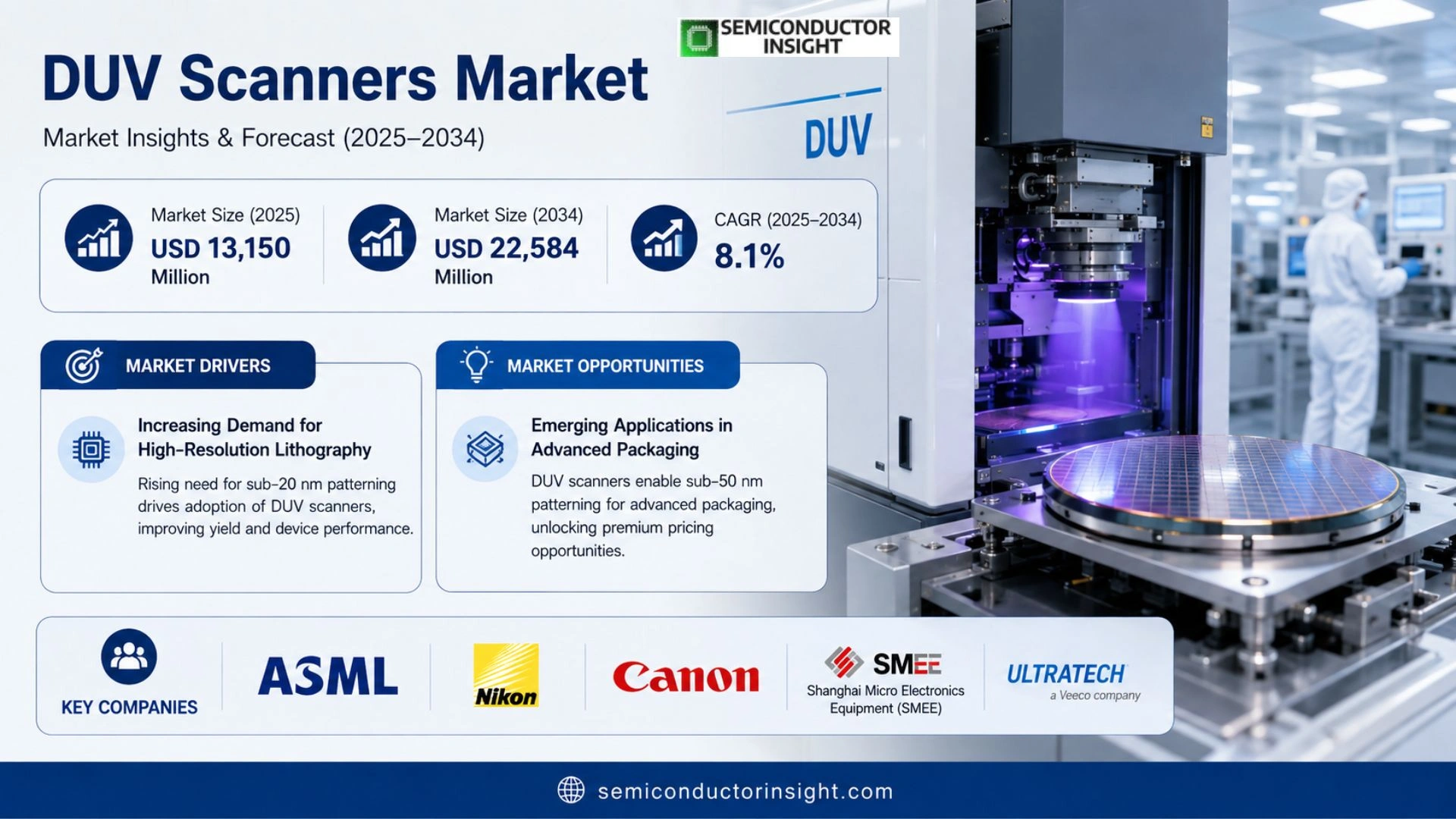
DUV Scanners market size was valued at USD 13,150 million in 2025. The market is projected to reach USD 22,584 million by 2034, exhibiting a CAGR of 8.1% during the forecast period.
DUV scanners are core lithography tools in semiconductor manufacturing that transfer circuit patterns from a mask onto wafers through step‑and‑scan projection with extremely high precision. Their value extends beyond exposure itself; they integrate 193 nm ArF immersion, 193 nm dry ArF and 248 nm dry KrF light‑source routes with projection optics, dual‑stage architecture, alignment metrology, focus & leveling control, temperature management and overlay control into platforms capable of sustained volume production.
The market expands because global capacity additions continue across advanced logic, DRAM, 3D NAND, CMOS image sensors and automotive chips. Policy initiatives such as the U.S. CHIPS Act and European Chips Act reinforce demand for both advanced immersion platforms and mature dry systems. Leading OEMs,ASML, Nikon, Canon and SMEE,maintain high barriers to entry through mastery of optics, motion control and long‑term service models, enabling foundries and IDMs to optimise yield, throughput and cost per pattern transfer.
MARKET DRIVERS
Increasing Demand for High‑Resolution Lithography
DUV Scanners market is being propelled by chipmakers’ quest for patterning accuracy below 20 nm. As device architectures shrink, manufacturers require finer line‑edge control, and deep‑ultraviolet tools deliver the photon energy necessary to etch tighter features without resorting to more complex extreme‑UV platforms. This shift translates into higher wafer yields and lower defect densities, directly affecting bottom‑line profitability.
Advances in Laser Source Technology
Recent breakthroughs in excimer‑laser efficiency have cut operational power consumption by roughly 12 %, while extending lamp life to beyond 20 million pulses. These engineering gains reduce total cost of ownership, prompting midsize fabs to upgrade from legacy i-line equipment to state‑of‑the‑art DUV scanners. The financial rationale is reinforced by a measurable lift in throughput,often 15 % per shift.
➤ “Clients that switched to the latest 193 nm scanner reported a 10 % reduction in cycle time, which translates into faster time‑to‑market for premium products.”
Beyond pure performance, the reliability of modern DUV systems eases maintenance schedules, allowing fab managers to allocate engineering resources toward process innovation rather than equipment downtime. This operational flexibility is increasingly viewed as a competitive advantage in a market defined by rapid product cycles.
MARKET CHALLENGES
Cost Sensitivity in Semiconductor Manufacturing
Although DUV scanners deliver decisive patterning precision, the capital outlay,often exceeding $30 million per unit,remains a hurdle for cost‑conscious fabs. When capacity expansion decisions are weighed against a volatile demand outlook, many operators defer investments until a clear ROI trajectory emerges.
Other Challenges
Supply Chain Volatility
The procurement of high‑purity gases and specialized optics is subject to geopolitical flux and raw‑material shortages. Disruptions inflate lead times, compelling manufacturers to stockpile components, which in turn ties up working capital and erodes margins.
MARKET RESTRAINTS
Stringent Environmental Regulations
Regulatory bodies across North America and Europe have tightened emissions standards for photolithography chemicals. Compliance mandates additional filtration systems and periodic reporting, inflating operational expenditures for DUV equipment owners.
Moreover, the growing emphasis on sustainability forces fabs to evaluate the lifecycle impact of excimer‑laser gases. The necessity to transition to greener alternatives without compromising photon flux adds a layer of technical complexity that can delay equipment adoption.
MARKET OPPORTUNITIES
Emerging Applications in Advanced Packaging
Advanced packaging techniques such as fan‑out wafer‑level chip‑scale packaging are demanding sub‑50 nm line widths, a regime where DUV scanners excel. Companies that re‑tool for these niche processes can capture premium pricing tiers and diversify revenue streams beyond traditional logic nodes.
Integration with AI‑Driven Process Control
Artificial‑intelligence algorithms are being embedded into scanner control loops to predict tool drift and adjust exposure parameters in real time. This synergy enhances yield predictability, lowers scrap rates, and creates a differentiated value proposition that could accelerate adoption of next‑generation DUV platforms.
Finally, collaborations between equipment manufacturers and foundry consortia are fostering standards that streamline tool qualification. Harmonized specifications reduce the time required for new scanners to enter production lines, unlocking faster market penetration for innovative designs.
DUV Scanners Market Trends
Immersion vs Dry Platform Shift
DUV scanner segment is experiencing a clear divergence between immersion systems targeting advanced logic nodes and dry scanners serving high‑volume, cost‑sensitive layers. Immersion platforms deliver superior overlay and pattern fidelity, which makes them indispensable for the most demanding 7‑nm and below nodes. In contrast, dry scanners dominate the production of mature logic, memory, and large‑area CMOS image sensors because they offer higher wafer throughput at lower ownership cost. This functional split allows fab operators to allocate capital efficiently, pairing premium immersion tools on critical layers while leveraging dry equipment for the bulk of transistor layers. Furthermore, the cost equation of dry scanners benefits from higher uptime and simpler maintenance, which translates into lower per‑wafer depreciation for high‑volume production lines. Consequently, fabs can scale output without proportionally increasing capex.
Other Trends
Regional Capacity Expansion
Policy initiatives across the United States, Europe and Japan are reshaping the geographic distribution of front‑end capacity. The CHIPS and Science Act, the European Chips Act and Japan’s METI roadmap each provide subsidies and tax incentives tied to the procurement of domestic lithography equipment. As a result, fabs in the Netherlands, Japan and mainland China continue to host the bulk of scanner installations, while new cleanrooms are being commissioned in the United States and South Korea to satisfy local content requirements. This trend creates a parallel demand stream: legacy dry tools for volume manufacturing and upgraded immersion platforms for high‑value nodes, both of which must be serviced by OEMs with strong regional support networks. The anticipated influx of new fabs also pressures OEMs to accelerate the rollout of next‑generation laser sources, ensuring that both immersion and dry platforms can meet tighter overlay windows while maintaining throughput.
OEM Competitive Landscape and Service Model
The supplier base remains concentrated among four major OEMs, each emphasizing a distinct value proposition. ASML distinguishes itself through a fully integrated portfolio that spans both immersion and dry architectures, coupled with a systematic upgrade path that extends the life of installed tools. Nikon focuses its messaging on overlay accuracy and wafer‑per‑hour rates, publishing detailed performance metrics that appeal to foundries seeking incremental productivity gains. Canon leverages wide‑field KrF designs to dominate the CIS segment, where high‑throughput exposure of large die sizes is critical. SMEE provides a domestic alternative for 90‑nm and larger nodes, supporting China’s strategy of reducing reliance on overseas equipment. The common business model blends equipment sale with long‑term service contracts, spare‑part provisioning and software optimisation, ensuring that revenue streams remain resilient even as semiconductor cycles ebb and flow. In practice, this hybrid service model reduces upfront financial exposure for customers and creates a predictable cash flow for suppliers, reinforcing the sector’s overall stability.
COMPETITIVE LANDSCAPE
Key Industry Players
Competitive dynamics of DUV scanners ecosystem in 2024
ASML remains the undisputed leader in DUV scanner arena, offering both immersion and dry families under the TWINSCAN brand. Its ability to retrofit installed tools with System Node Enhancement Packages gives customers a pathway to extend platform relevance across successive logic generations, thereby safeguarding capital efficiency. The company’s extensive service network and deep integration of alignment metrology, temperature control, and overlay management have turned each shipment into a long‑term revenue stream anchored on uptime and throughput guarantees. Foundries such as TSMC and Intel rely heavily on ASML’s dual‑stage architecture to meet the overlay precision demanded by advanced 7 nm and beyond nodes, reinforcing the OEM’s bargaining position and margin resilience.
Beyond the market leader, Nikon and Canon provide credible alternatives that focus on distinct value propositions. Nikon’s portfolio stresses overlay accuracy and wafers‑per‑hour metrics, targeting high‑volume logic and memory fabs that prioritize yield stability. Canon, with its wide‑field KrF scanners, excels in CIS and automotive sensor production where throughput outweighs resolution extremes. Chinese OEM SMEE has introduced the SSX600 series, positioning itself as a cost‑effective option for 90 nm‑110 nm processes and attracting domestic fabs seeking supply‑chain independence. Smaller specialists such as Ultratech (Veeco), Gigaphoton, SUSS MicroTec, and Tokyo Electron contribute niche capabilities,ranging from high‑NA optics to proprietary illumination sources,that allow them to capture segments focused on specialty devices, mature nodes, or advanced packaging. Their limited install base is offset by aggressive after‑sale service models and collaborations with regional foundries, creating a fragmented yet strategically important second tier.
List of Key DUV Scanners Companies Profiled
- ASML
- Nikon Corporation
- Canon Inc.
- Shanghai Micro Electronics Equipment (SMEE)
- Ultratech (Veeco)
- Gigaphoton
- SUSS MicroTec
- Tokyo Electron Limited
- Lumentum
- JEOL Ltd.
- Advantest Corporation
- Hitachi High‑Technologies
Segment Analysis:
| Segment Category | Sub-Segments | Key Insights |
| By Type |
|
193 nm Immersion Scanners are viewed as the leading sub‑segment because they combine high resolution with superior overlay capability.
|
| By Application |
|
Logic Chip Manufacturing drives the most sophisticated DUV scanner requirements.
|
| By End User |
|
Foundries are the dominant end‑user segment because they operate at the highest production scale and demand long‑term service models.
|
| By Technology Route |
|
ArF Scanners retain primacy due to their balance of resolution and throughput across both immersion and dry platforms.
|
| By Exposure Medium |
|
Immersion Scanners dominate the high‑value segment because they deliver superior imaging performance for the most demanding layers.
|
Regional Analysis: DUV Scanners Market
North America
Leading chipmakers allocate a disproportionate share of their capital budgets to DUV Scanners, prioritising upgrades that enable sub‑50 nm patterning. Investment decisions are increasingly linked to product road‑maps for high‑performance computing, where processing speed hinges on lithographic precision.
Environmental compliance frameworks in the United States impose strict emissions standards on laser‑based equipment. Suppliers respond by integrating energy‑recovery modules, a move that simultaneously satisfies regulators and reduces operating expense for end users.
Recent geopolitical frictions have prompted North‑American fabs to diversify component sourcing. Strategic stockpiling of critical optics and on‑shore manufacturing of key sub‑assemblies mitigate the risk of sudden shortages.
Early adopters in the automotive and 5G sectors favour DUV Scanners that deliver tighter line‑edge roughness. This preference drives OEMs to co‑develop custom tool configurations that align with specific wafer‑size requirements.
Europe
European semiconductor clusters, particularly in Germany and the Netherlands, are intensifying their focus on DUV technology as a bridge toward extreme‑ultraviolet adoption. Policymakers are leveraging Horizon‑Europe funds to subsidise joint‑venture R&D projects, which in turn cultivates a talent pool adept at precision optics. Manufacturers are also responding to stringent EU environmental directives by offering refurbished‑scanner programs that extend equipment lifecycles while curbing waste. The net effect is a market environment where collaboration supersedes competition, and where cost‑competitiveness is derived from shared innovation rather than volume discounts.
Asia‑Pacific
The Asia‑Pacific region, anchored by Taiwan, South Korea, and Japan, remains a hotbed for high‑volume DUV Scanner deployment. Local fabs benefit from an entrenched ecosystem of supply‑chain partners that deliver rapid prototyping of photomasks and ancillary optics. Cultural emphasis on continuous improvement drives incremental upgrades to existing DUV lines, ensuring that throughput gains keep pace with aggressive product‑launch calendars. However, talent scarcity in advanced photolithography engineering forces many players to recruit expatriates, creating a subtle competitive edge for firms that can attract cross‑border expertise.
South America
South American semiconductor activity is modest but strategically evolving, with Brazil spearheading initiatives to develop an indigenous DUV Scanner maintenance capability. Government incentives encourage joint ventures between local universities and foreign equipment vendors, fostering a nascent cadre of specialists in laser alignment and defect inspection. While the market size is limited, the emphasis on self‑sufficiency reduces reliance on imports and lays groundwork for future capacity expansion as regional demand for IoT devices escalates.
Middle East & Africa
In the Middle East and Africa, DUV Scanners market is still in an exploratory phase. Emerging fab projects in the United Arab Emirates and South Africa view DUV platforms as the most viable entry point for establishing domestic chip production. Partnerships with established North‑American suppliers are framed around technology transfer and training programs, reflecting a long‑term ambition to develop a skilled workforce. The prevailing narrative is one of cautious optimism, with stakeholders prioritising knowledge acquisition over immediate scale.
Report Scope
This market research report provides a comprehensive analysis of the DUV Scanners Market , covering the forecast period 2026–2034. It offers detailed insights into market dynamics, technological advancements, competitive landscape, and key trends shaping the industry.
Key focus areas of the report include:
- Market Overview: The report begins with an overview outlining its current market scenario, key growth indicators, and industry transformation drivers. It discusses macroeconomic factors, demand–supply balance, regulatory landscape, and the strategic role of semiconductors in powering advancements across industries such as automotive, telecommunications, consumer electronics, and industrial automation.
- Market Size & Forecast: Historical data and future projections for revenue, unit shipments, and market value across major regions and segments.
- Segmentation Analysis: Detailed breakdown by product type, technology, application, and end-user industry to identify high-growth segments and investment opportunities.
- Regional Insights: Insights into market performance across North America, Europe, Asia-Pacific, Latin America, and the Middle East & Africa, including country-level analysis where relevant.
- Competitive Landscape: Profiles of leading market participants, including their product offerings, R&D focus, manufacturing capacity, pricing strategies, and recent developments such as mergers, acquisitions, and partnerships.
- Technology Trends & Innovation: Assessment of emerging technologies, integration of AI/IoT, semiconductor design trends, fabrication techniques, and evolving industry standards.
- Market Drivers & Restraints: Evaluation of factors driving market growth along with challenges, supply chain constraints, regulatory issues, and market-entry barriers.
- Stakeholder Insights: Insights for component suppliers, OEMs, system integrators, investors, and policymakers regarding the evolving ecosystem and strategic opportunities.
Primary and secondary research methods are employed, including interviews with industry experts, data from verified sources, and real-time market intelligence to ensure the accuracy and reliability of the insights presented.
FREQUENTLY ASKED QUESTIONS:
What is the current market size of DUV Scanners Market?
-> DUV Scanners market is projected to reach USD 22,584 million by 2034, exhibiting a CAGR of 8.1% during the forecast period.
Which key companies operate in DUV Scanners Market?
-> Key players include ASML, Nikon Corporation, Canon Inc., and Shanghai Micro Electronics Equipment (SMEE) Co., Ltd.
What are the key growth drivers?
-> Key growth drivers include rising demand for advanced logic and memory chips, reshoring of semiconductor manufacturing, policy support such as the CHIPS and Science Act and European Chips Act, and expansion of mature‑node capacity and specialty processes.
Which region dominates the market?
-> Asia‑Pacific dominates DUV Scanners market, driven by high fab density in China, Japan, and South Korea, while Europe and North America also show strong demand.
What are the emerging trends?
-> Emerging trends include continuous upgrades of immersion platforms, cost‑effective dry scanner deployments for high‑volume layers, increased focus on CMOS image sensor applications, and domestic substitution initiatives in China.

Get Sample Report PDF for Exclusive Insights
Report Sample Includes
- Table of Contents
- List of Tables & Figures
- Charts, Research Methodology, and more...
 Download Sample Report PDF