Key Statistics
Key Takeaways
- European market trajectory: The Europe silicon carbide wafer market is valued at USD 647.63 million in 2025 and is forecast to reach USD 4,283.97 million by 2034, expanding at 23.4% during 2026–2034 as substrate and epitaxial capacity serves automotive and industrial power electronics.
- Six-inch substrate leadership: The 6 Inch format accounts for an estimated ~48% of 2025 European revenue, reflecting established qualification at 150 mm, while the Others category, including the expanding 200 mm generation, advances at an estimated ~28.7% annual rate from a smaller base.
- Power-device applications: Power Device is the largest end-use category at an estimated ~65% of wafer demand, driven by high-voltage automotive converters and industrial switching, whereas specialized optoelectronics and wireless programs sustain smaller, more specification-sensitive procurement channels.
- German industrial concentration: Germany represents an estimated ~35% of European market demand and a modeled ~24.0% annual growth path; France and the United Kingdom each account for ~14%, but differ materially in substrate engineering and downstream manufacturing profiles.
- Yield, qualification and cost: Substrate defect density, wafer bow, polishing quality and long automotive approval cycles restrain commercial throughput even as European investment moves from 150 mm toward 200 mm production; equipment installation does not immediately translate into qualified wafer shipments.
Europe Silicon Carbide Wafer Market Overview
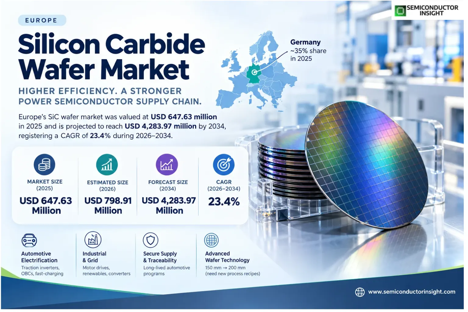
Europe silicon carbide wafer market was valued at USD 647.63 million in 2025, is estimated at USD 798.91 million in 2026, and is projected to reach USD 4,283.97 million by 2034, registering a CAGR of 23.4% over 2026–2034. Germany is the largest country market, with an estimated ~35% share in 2025, supported by substrate fabrication, power electronics and automotive qualification.
Silicon carbide wafers provide the crystalline platform for power semiconductors that operate at higher electric fields and temperatures than conventional silicon alternatives. The substrate may be cut from bulk SiC crystal and polished for epitaxial deposition, or engineered to carry a thin high-quality active layer over a supporting base. European purchasers specify wafer diameter, crystallographic orientation, defect density, resistivity, surface finish and thickness uniformity before a substrate enters device fabrication.
The European revenue boundary includes silicon carbide semiconductor substrates and qualifying epitaxial wafers supplied for use in the region, including appropriate internal supply attributed to the broad wafer market. It excludes finished MOSFETs, power modules, inverters, vehicles, wafer boats and deposition machinery. This distinction matters because a single automotive traction inverter can embody several value-chain stages, while the wafer is sold or transferred much earlier in the manufacturing process.
A shift from 150 mm to 200 mm material changes wafer economics without eliminating difficult materials-science constraints. A larger disk offers more die sites per processing cycle, but crystal growth, slicing, grinding and chemical-mechanical polishing must maintain uniformity over a wider surface. Device makers also need new process recipes and yield evidence before migrating production, so the capacity announcements of equipment makers should be distinguished from repeatable sales of accepted semiconductor-grade wafers.
Automotive electrification is the principal demand mechanism, as traction inverters, onboard chargers and fast-charging infrastructure use SiC switching devices to reduce energy losses and cooling requirements. Industrial motor drives, grid converters and renewable-energy systems add demand with different reliability and procurement schedules. In Europe, purchasing decisions also depend on secure materials access and the ability to trace substrates through long-lived automotive programs that may outlast an individual fabrication technology generation.
The competitive setting is being reshaped by integrated investment and engineered substrates rather than wafer volume alone. STMicroelectronics is building a Catania supply chain that connects material growth to device fabrication, while German and French specialists pursue substrate production and reusable engineering approaches. European chip policy can encourage domestic capacity, but near-term revenue depends on yields, customer qualification and utilization rather than the headline size of announced projects.
Segment Analysis: By Type
By Products Type, European silicon carbide wafer demand spans 2 Inch, 3 Inch, 4 Inch, 6 Inch and Others. The 6 Inch class is the largest at an estimated ~48% of 2025 revenue; Others contributes ~20% and includes the emerging 200 mm generation, modeled at ~28.7% CAGR, while 4 Inch retains ~20% through specialty and legacy production lines.
| Products Type | Technical role | Market position |
|---|---|---|
| 2 Inch | Two-inch substrates are primarily associated with older processing equipment, prototype circuits and low-volume experimental runs where the material cost per wafer is less important than access to a qualified recipe. Universities and specialist device laboratories can continue ordering these small formats when changing the chuck, mask set and thermal processing flow would consume more engineering resources than the project can justify. | The 2 Inch category represents an estimated ~4% of European revenue in 2025 and a modeled ~8.0% annual growth rate. Its commercial importance is not mass-market wafer volume but the availability of small-lot materials for device proof-of-concept, calibration and niche high-temperature electronics. The category loses relative share as production economics increasingly favor larger disks. |
| 3 Inch | Three-inch SiC wafers bridge historical compound-semiconductor production with specialized power and radio-frequency processes. Some tools remain configured for this diameter because the capital expense of retooling cannot be recovered from a small or mature product family. The format can support unusual specifications or research orders that would be uneconomic to move immediately into a high-throughput automotive fabrication line. | An estimated ~8% share in 2025 places 3 Inch substrates below the principal commercial diameters, with modeled ~11.0% growth as specialty programs continue. Buyers value stable defect specifications and repeatable small-volume delivery more than the lowest cost per usable die. Suppliers face a shrinking addressable base of legacy tools, which limits the segment’s contribution to the broader European expansion. |
| 4 Inch | Four-inch wafers remain relevant where industrial electronics and specialized devices use established process recipes. The smaller diameter reduces absolute material requirements for low-volume products and can simplify engineering transfers between pilot facilities, but it limits the number of dies processed per tool cycle. Manufacturers that already operate these lines may continue buying qualified 100 mm substrates while investing separately in larger-diameter programs. | The 4 Inch segment holds an estimated ~20% of the 2025 market and a modeled ~17.0% CAGR, reflecting a substantial installed process base that is not yet obsolete. Its advantage is process familiarity, particularly when device qualification is costly or demand is fragmented. Over the forecast period, however, new high-volume automotive awards tend to favor more productive wafer formats. |
| 6 Inch | Six-inch substrates, equivalent to the 150 mm class, underpin many established commercial SiC device lines. The diameter offers a workable balance between boule yield, epi uniformity, fabrication equipment availability and output per run. Automotive suppliers can qualify this platform against thermal cycling and reliability specifications, while sourcing teams can compare established producers on defect distribution, delivery consistency and effective cost per usable device. | Largest category (~48% share in 2025). A modeled ~25.0% growth path reflects the continuing conversion of vehicle and industrial switching to SiC alongside capacity utilization gains. The installed 150 mm process ecosystem provides immediate demand even as new 200 mm equipment is installed. Its share may gradually decline, but absolute shipments can continue expanding strongly through the transition. |
| Others | The Others category captures diameters and engineered formats outside the named 2, 3, 4 and 6 Inch groups, including commercial 200 mm substrates and qualifying nonstandard pilot formats. Larger wafers require substantial advances in crystal-growth yield, slicing damage control and epi uniformity. Engineered SiC platforms can also separate an expensive active layer from the supporting substrate, changing material utilization and cost structure. | The category accounts for an estimated ~20% of 2025 revenue and is modeled as the fastest-growing at ~28.7% CAGR, led by the 200 mm transition rather than a sudden replacement of mature lines. Adoption depends on actual qualified output and customer process conversion, not the nominal diameter of equipment. Early capacity can command value before achieving the utilization of 150 mm facilities. |
Additional segmentation: Country
Country demand is assessed separately from wafer diameter because Germany, France, the United Kingdom, Italy, Spain, the Netherlands and Belgium play different roles in the European SiC ecosystem. Germany combines wafer production with vehicle power electronics, France emphasizes engineered materials, and Italy contains integrated fabrication investment. The remaining markets are smaller but supply specialized equipment, research and purchasing channels that affect material qualification.
| Country | 2025 estimated share | Commercial role |
|---|---|---|
| Germany | ~35% | SiC substrate production and automotive qualification |
| United Kingdom | ~14% | Specialty electronics and industrial design programs |
| France | ~14% | Engineered substrate research and materials partnerships |
| Italy | ~13% | Integrated SiC fabrication and epitaxial demand |
| Spain | ~10% | Power electronics procurement and energy applications |
| Netherlands | ~8% | Equipment and specialized electronics supply |
| Belgium | ~6% | Semiconductor research and pilot activity |
Segment Analysis: By Application
By Application, Power Device is the leading category at an estimated ~65% of European SiC wafer revenue in 2025, followed by Electronics & Optoelectronics (~17%), Wireless Infrastructure (~10%) and Others (~8%). Power Device is modeled at ~24.0% CAGR, with the Others group growing faster at ~27.0% from a smaller base as niche specifications broaden.
| Application | Demand characteristics |
|---|---|
| Power Device | Largest application (~65%). Silicon carbide substrates support the MOSFETs and diodes used in traction inverters, charging systems, solar converters and industrial power drives. These customers purchase wafers through strict qualification chains because a crystal defect can reduce device yield or long-term electrical reliability. The segment is modeled to expand at ~24.0% annually as vehicle architectures move to higher voltages and factory power systems demand greater conversion efficiency. |
| Electronics & Optoelectronics | This category combines specialized electronic components with optoelectronic devices whose process requirements differ from mainstream automotive power transistors. Smaller wafer lots may carry unusual surface, doping or defect specifications and can justify higher testing effort. The modeled ~17% share in 2025 and ~21.0% annual growth reflect continuing demand for engineered materials, although product qualification and device mix prevent the same scale economics found in traction power. |
| Wireless Infrastructure | Wireless applications draw on semi-insulating or other specialty SiC substrates where thermal conductivity and radio-frequency behavior influence amplifier design. Their procurement cycle depends on telecom equipment refreshes, defense communications and specialized microwave systems rather than EV registrations. With an estimated ~10% of European wafer demand and ~19.0% modeled CAGR, this segment remains strategically important despite a smaller purchasing base and stringent electrical-material requirements. |
| Others | Other uses include research devices, sensors, high-temperature electronics and emerging semiconductor experiments that do not fit the named application groups. Orders often involve custom growth or epitaxial conditions and a development stage before repeatable production. The category is estimated at ~8% of 2025 revenue but carries a modeled ~27.0% annual growth rate as qualification activity diversifies, while remaining too fragmented to rival power-device volume. |
European wafer channels are shaped by long qualification cycles rather than spot commodity trading. A substrate supplier must demonstrate defect mapping, lot-to-lot repeatability and traceability, while epitaxial partners must preserve film thickness and doping control across the intended wafer diameter. Automotive buyers generally validate the final semiconductor and system performance, making upstream material approval an indirect but powerful purchasing gate for both merchant and integrated supply.
Regional Analysis
European silicon carbide wafer purchasing is concentrated in Germany (~35%), followed by the combined Spain, Netherlands and Belgium cluster (~24%), France (~14%), the United Kingdom (~14%) and Italy (~13%). Germany is modeled to grow at ~24.0% CAGR, Italy at ~24.5%, France at ~23.0%, the United Kingdom at ~22.0% and the three-country cluster at ~22.7%, reflecting different roles in the materials chain.
Which European locations combine qualified wafer demand with manufacturing investment?
Country market positions depend on both the physical location of substrate production and the location of downstream device procurement. Germany has a mature automotive and wafer-manufacturing base; Italy is investing in an integrated SiC chain; France contributes engineered-substrate technology; the United Kingdom has smaller specialty electronics channels. Spain, the Netherlands and Belgium form a distributed cluster where industrial conversion, equipment and research influence purchasing decisions rather than one dominant crystal-growth campus.
The model uses five European country-cluster blocks so that the regional analysis covers the same European geography as the publisher market. Germany represents the largest single-country allocation at ~35%, while France and the United Kingdom each hold ~14% despite very different industrial structures. Italy is ~13%, and Spain, the Netherlands and Belgium together contribute ~24%; the seven individual countries remain separately visible in the Country segmentation axis.
| Region | Position | Growth outlook | Demand profile | What decides supplier selection |
|---|---|---|---|---|
| Germany | Largest market (~35%) | Modeled ~24.0% CAGR | Automotive qualification and SiC substrate production | Consistent boule and polished-wafer quality, long-term supply agreements and traceable automotive lots |
| France | Materials innovation (~14%) | Modeled ~23.0% CAGR | Engineered substrates and research partnerships | Defect reduction, bonding performance and compatibility with European device process flows |
| United Kingdom | Specialty demand (~14%) | Modeled ~22.0% CAGR | Industrial electronics and design-led procurement | Availability of custom specifications, engineering support and dependable lower-volume supply |
| Italy | Integrated capacity (~13%) | Modeled ~24.5% CAGR | Catania power-device manufacturing ecosystem | Qualified epitaxial input, yield stability and coordinated substrate-to-device capacity ramps |
| Spain, Netherlands & Belgium | Distributed cluster (~24%) | Modeled ~22.7% CAGR | Energy conversion, equipment and research | Technical documentation, delivery flexibility and participation in collaborative pilot programs |
Europe Silicon Carbide Wafer Market Competitive Landscape
Competition in European SiC wafers involves integrated semiconductor manufacturers, specialized crystal growers and engineered-substrate developers. STMicroelectronics, ROHM-linked SiCrystal and Coherent have different manufacturing and supply-chain positions, while Soitec focuses on engineered materials. Equipment companies and historical corporate names appear in the wider ecosystem but should not be presented as current independent merchant substrate leaders.
The most direct rivalry concerns the ability to supply low-defect wafers at a diameter and specification that customers can qualify in their existing process. Substrate pricing is only one variable; effective cost per good device also depends on epitaxial uniformity, crystal defects, wafer flatness and handling losses. Suppliers with strong materials characterization and repeatable deliveries can retain programs even when nominal wafer prices fall during a capacity expansion.
Integrated manufacturers can coordinate crystal growth, epitaxy and power-device fabrication, potentially improving process feedback and security of supply. STMicroelectronics is pursuing that structure in Italy, while ROHM owns SiCrystal in Germany. The commercial model differs from a pure merchant supplier because some wafers move internally; European market sizing should therefore reflect the broad qualifying wafer value without treating downstream device revenue as another wafer sale.
Coherent participates through SiC materials and epitaxial products, with its 200 mm n-type epi-wafer platform adding technical options for global device makers. Soitec seeks to change the substrate architecture through SmartSiC, including collaboration with materials partners. These approaches compete on different points of the value chain: crystal quality and epi uniformity on one side, and engineered utilization of premium active material on the other.
The company list also contains names that require corporate or product-role clarification. Norstel was acquired by STMicroelectronics and should not be counted as an independent current supplier, while II-VI is now Coherent. LPE is associated with epitaxy equipment rather than merchant SiC substrates; branch or regional labels for Toshiba, ROHM, Nippon Carbon and Aymont do not by themselves prove European wafer manufacturing. Such distinctions prevent inflated supplier counts.
Tier structure
| Tier | Companies | Basis of competition |
|---|---|---|
| Tier 1 — integrated | STMicroelectronics; SiCrystal / ROHM | Integrated ownership provides direct links between substrate development, epitaxial processing and downstream power-device qualification. The main advantage is process feedback and predictable long-term material access, while capital intensity and internal capacity allocation can limit flexibility for outside wafer buyers. These firms compete through manufacturing execution and the reliability of the complete device-material chain. |
| Tier 2 — specialist materials | Coherent; Soitec | Specialist producers and engineered-wafer developers emphasize substrate properties, epitaxial quality or alternative material architectures. Their position depends on demonstrating lower defects, compatible fabrication behavior and commercially viable yields at the target diameter. A materials partnership or development platform may influence future competition without automatically creating an independent European high-volume crystal-growth facility. |
| Adjacent and historical | LPE; AIXTRON; Norstel; II-VI; Toshiba; Nippon Carbon; Aymont Technology | This group combines equipment vendors, former independent names and regional business references that require careful interpretation. AIXTRON and LPE support wafer processing through equipment; Norstel belongs to STMicroelectronics and II-VI is Coherent. The remaining names may participate through materials or customer channels, but the available evidence does not justify classifying each as an independent leading European merchant SiC wafer manufacturer. |
Key companies profiled
- STMicroelectronics
- Infineon Technologies
- SiCrystal GmbH (ROHM group)
- Norstel AB (STMicroelectronics)
- II-VI Incorporated (Coherent)
- LPE SpA
- Nippon Carbon
- Toshiba
- ROHM
- Aymont Technology
- Coherent
- Soitec
- AIXTRON
Europe Silicon Carbide Wafer Production Capacity Analysis
European SiC wafer capacity is evolving from established 150 mm production toward qualified 200 mm material, with investment concentrated in crystal growth, epitaxy and integrated power-device campuses. Announced factory output should be interpreted as a future engineering target, not realized sales. The binding constraint is often the number of wafers that pass defect, thickness and electrical acceptance criteria rather than the nominal number of tool positions.
The Catania program illustrates the complexity of scaling an integrated materials chain. Crystal-growth furnaces, slicing and polishing lines, epitaxial reactors and device fabrication tools must be synchronized so that each stage receives the correct specification at the right volume. STMicroelectronics announced a long-term capacity plan, but commercial output can rise unevenly as tools are commissioned and process yields improve. A ramp in one stage may temporarily outpace the next.
German production and research capabilities add a different capacity profile. SiCrystal operates a crystal-wafer business in Nürnberg, while Fraunhofer IISB documents silicon carbide services and pilot work relevant to larger diameters. These activities can strengthen process knowledge and local supply resilience, but pilot tools do not provide the same predictable wafer output as qualified production lines. The practical capacity measure is repeatable accepted lots over several customer cycles.
Epitaxy equipment throughput is an additional limit because the active film must meet doping and thickness tolerances across the whole wafer. AIXTRON describes G10-SiC configurations for 150 mm and 200 mm material, but tool shipments represent manufacturing investment rather than wafer revenue. Larger-diameter transitions may initially lower utilization as operators tune process uniformity, which makes commercial capacity growth slower than the installation of new reactors.
Europe Silicon Carbide Wafer Market Dynamics
Demand growth reflects the move toward higher-efficiency power conversion, European semiconductor investment and the transition to larger wafer formats. The principal constraints remain expensive crystal growth, defect-driven yield loss and long qualification periods. Commercial opportunity is strongest where manufacturers can translate 200 mm materials progress into repeatable production rather than relying solely on planned capacity or broad industrial policy announcements.
MARKET DRIVERS
Drivers Impact Analysis*
| Market Drivers | Impact Rank | CAGR Contribution (%) | 2026–2028 | 2029–2031 | 2032–2034 |
|---|---|---|---|---|---|
| EV traction inverter and onboard charger demand | High | +8.20% | High | High | Medium |
| Industrial and renewable power conversion | High | +6.30% | High | High | High |
| 200 mm wafer process migration | Medium-High | +5.00% | Medium | High | High |
| European integrated manufacturing investment | Medium | +3.80% | High | High | Medium |
| Engineered-substrate cost improvements | Low-Medium | +2.70% | Low | Medium | High |
| Others (research orders, power grids, specialty RF, domestic sourcing) | Low | +1.80% | Medium | Medium | Low |
Vehicle power electronics raises wafer specifications
Electric vehicles place demanding efficiency and thermal requirements on traction inverters and onboard chargers, making silicon carbide a useful alternative to silicon in many high-voltage switching designs. The upstream effect is a need for wafers with low defect density and stable electrical characteristics, because failures at the substrate stage can undermine expensive device processing. European automotive qualification cycles favor suppliers that can demonstrate consistent material performance over repeated lots.
Industrial conversion adds a diversified demand base
Factories, grid equipment and renewable-energy systems use power conversion under duty cycles that differ from automotive applications. SiC devices can reduce switching losses and cooling needs in these systems, providing wafer demand that is not tied to a single vehicle launch calendar. The breadth of applications helps substrate producers manage demand fluctuations, although industrial customers still require robust reliability data and competitive total system cost.
Larger wafers improve potential device economics
A 200 mm wafer offers more surface area than a 150 mm disk, which can lower processing cost per die if crystal quality and downstream yield remain high. That condition is essential: a larger defective area or poor epitaxial uniformity can erase the theoretical productivity gain. European producers are investing in new tools and materials programs, but the full economic benefit arrives only after process recipes and inspection methods stabilize.
Local manufacturing improves supply assurance
Integrated European SiC investment gives automotive and industrial buyers an option to reduce exposure to long overseas materials chains. A domestic substrate source can shorten engineering communication and support traceability across crystal, epi and device stages. However, local origin does not automatically win a contract; the supplier must still meet defect limits, commercial price targets and delivery schedules over a multiyear production program.
MARKET RESTRAINTS
Restraints Impact Analysis*
| Market Restraints | Impact Rank | CAGR Contribution (%) | 2026–2028 | 2029–2031 | 2032–2034 |
|---|---|---|---|---|---|
| Defect-related wafer and epitaxial yield losses | High | -1.80% | High | Medium | Medium |
| Capital cost and energy intensity of crystal growth | Medium-High | -1.30% | High | High | Medium |
| Long automotive qualification and 200 mm transfers | Medium | -0.90% | High | Medium | Low |
| Others (supply concentration, inspection costs, demand volatility) | Low | -0.40% | Medium | Medium | Medium |
Crystal defects can destroy downstream value
Micropipes, dislocations and other defects in silicon carbide material can affect the breakdown behavior and reliability of power devices. Because processing adds value after the wafer is purchased, poor incoming material quality imposes costs beyond the substrate invoice. Suppliers must invest in inspection and crystal-growth control to achieve commercially acceptable yield, and customers may delay approval until defect performance is demonstrated across production lots.
Manufacturing costs remain structurally high
SiC crystal growth requires specialized high-temperature equipment, energy and long processing times, followed by slicing, polishing and potentially epitaxial deposition. A larger wafer does not eliminate these cost components, particularly during an early yield ramp. Capital commitments can pressure suppliers to seek volume before customers finish qualification, creating periods when installed capacity rises faster than profitable shipments.
Diameter changes trigger requalification
Migrating from 150 mm to 200 mm is not simply a purchase of larger substrates; handling, metrology, epitaxy and device process conditions can all change. Automotive customers must verify that the resulting devices retain electrical performance and lifetime reliability. This makes the transition commercially slower than equipment delivery announcements imply and may preserve demand for mature wafer sizes well into the forecast period.
Procurement concentration raises negotiation pressure
A limited group of large power-device manufacturers controls many high-volume qualification decisions, giving buyers leverage over substrate specifications, prices and delivery commitments. Materials suppliers may need to reserve capacity for a customer before final device approval, exposing them to schedule risk. The issue is most acute when a new wafer platform has few alternative qualified customers and limited opportunities to redirect output.
MARKET OPPORTUNITIES
SmartSiC can alter premium material utilization
Engineered substrates that transfer a thin active layer onto a supporting material offer a potential route to use expensive crystalline SiC more efficiently. This creates an opportunity for materials innovators to compete on total processed-wafer cost rather than conventional boule scale alone. Adoption will depend on interface integrity, high-temperature compatibility and device yields demonstrated in customer production, making qualification partnerships commercially important.
European supply chains can differentiate on traceability
Vehicle manufacturers and industrial power-system suppliers increasingly require clear component origin and reliable supply planning for long-lived platforms. European wafer producers can differentiate through material genealogy, lot-level defect maps and coordinated change control across the substrate and epitaxy stages. Such services are difficult to evaluate through headline wafer pricing but can reduce qualification risk and improve the durability of customer relationships.
Pilot capacity can shorten the learning cycle
Research centers and equipment developers offer opportunities to test larger wafer formats and specialized epi processes before a manufacturer commits to a full commercial line. Collaborative trials can reveal surface and doping problems earlier, lowering the cost of subsequent scale-up. These activities support technology development without being counted as mass-market wafer shipments, and their economic value comes from faster learning rather than immediate output.
Power infrastructure broadens the customer mix
High-efficiency conversion in renewable-energy installations, storage systems and industrial drives can provide demand outside automotive traction. A supplier qualified for one power-device platform may be able to serve adjacent voltage classes or packaging configurations if substrate specifications remain compatible. Diversifying the customer base reduces dependence on a few vehicle programs, although each new application still requires its own device-level validation.
Europe Silicon Carbide Wafer Supply Chain Analysis
The European SiC wafer chain starts with high-purity feedstock and crystal growth, proceeds through slicing, polishing and epitaxial deposition, and then supplies device fabs that convert the material into power and specialty semiconductors. A defect introduced early can propagate through multiple costly stages. The strongest commercial relationships therefore integrate technical inspection, long-term qualification and reliable volume scheduling rather than treating wafers as interchangeable commodities.
Upstream materials. SiC crystal quality depends on feedstock purity, temperature control and stable growth conditions, making the upstream stage a determinant of eventual device yield. Producers need reliable consumables and process equipment because interruptions can affect crystal consistency across a batch. European procurement strategies increasingly consider the resilience of this input chain alongside material specifications, particularly when customers expect wafer deliveries throughout a long automotive production cycle.
Wafer processing. After growth, crystal boules are sliced and polished to tight dimensional and surface standards, then may receive epitaxial layers tailored to device voltage and conductivity requirements. Damage or nonuniformity introduced during these steps can become expensive scrap after device fabrication. Inspection systems and repeatable polishing processes are therefore central to supplier economics, especially when a line is being transferred to a larger diameter.
Qualification and channels. Merchant wafer suppliers sell to device makers that have approved specific material grades, while integrated groups can move qualifying substrates internally under coordinated production plans. Development lots establish process compatibility before recurring orders begin. Because switching sources can trigger electrical and reliability requalification, suppliers that maintain detailed traceability and responsive engineering support may preserve business despite competition on the nominal wafer price.
Device customers. Power-device manufacturers translate substrate quality into usable MOSFETs and diodes for automotive, industrial and energy-conversion applications. Their fabrication yield determines how much material is needed to meet downstream demand, so improved wafer quality can reduce purchased units even while device output grows. Commercial forecasting must therefore distinguish demand for SiC devices from the value of wafers entering the manufacturing process.
Recent Developments in the Europe Silicon Carbide Wafer Market
- 3 June 2026 Published
The European Commission published a Chips Act 2.0 proposal intended to strengthen strategic semiconductor manufacturing capacity and industrial resilience. The initiative provides a policy setting for materials and equipment investment, but it is not a quantified order for silicon carbide substrates. Wafer suppliers may benefit indirectly if funded manufacturing programs adopt qualifying SiC processes and complete customer qualification. Source - 9 February 2026 Announced
The European Union announced support for the NanoIC pilot line in Belgium, highlighting continued investment in semiconductor research and pilot manufacturing. The facility serves a wider advanced-chip agenda rather than a dedicated SiC substrate factory. Its relevance to the wafer ecosystem is therefore the potential development of transferable inspection and process skills, not immediate European merchant SiC wafer revenue. Source - 3 December 2025 Announced
Coherent disclosed 300 mm silicon carbide platform capabilities directed primarily toward thermal-management applications for artificial intelligence and data-center equipment. The announcement demonstrates how SiC processing expertise can extend beyond power-device substrates, but the stated application is adjacent to the market considered here. It should not be interpreted as evidence that 300 mm power-semiconductor wafers have reached mass-market European qualification. Source - 22 September 2025 Announced
AIXTRON announced its 100th G10-SiC epitaxy-system shipment, marking a manufacturing-equipment milestone relevant to the expansion of SiC epitaxial capacity. The reactor family supports large-diameter processing, but an equipment delivery is not equivalent to a shipment of accepted epiwafers. Commercial materials output depends on installation, process tuning, device-fab acceptance and sustained production yields. Source - 13 February 2025 Announced
Infineon reported a milestone in releasing 200 mm silicon carbide products from its Villach manufacturing operation to customers. The development indicates progress in larger-diameter device processing within Europe, although finished SiC components are downstream of the wafer market. For substrate suppliers, the signal is a stronger technical pathway toward qualified 200 mm material and associated epitaxial requirements. Source - 26 September 2024 Announced
Coherent introduced 200 mm n-type silicon carbide epitaxial wafers, emphasizing thickness and doping uniformity for power semiconductor applications. The product development expands the available technical supply options for device makers seeking to transition from 150 mm. It does not establish a European-only production volume, but it demonstrates commercial attention to material specifications required for the larger wafer generation. Source - 24 September 2024 Announced
Soitec and Resonac announced a joint development agreement concerning 200 mm SmartSiC engineered substrates for next-generation electric vehicles. The program links thin-layer substrate architecture with the demanding qualification needs of automotive power semiconductors. Market adoption will depend on electrical performance, mechanical integrity and economic benefit over conventional wafers, rather than solely on the announcement of a materials partnership. Source - 22 May 2024 Announced
Soitec and Tokai Carbon announced a strategic partnership to develop polycrystalline SiC base substrates for engineered SmartSiC wafers. This arrangement addresses an upstream material component of a proposed alternative wafer architecture, where a supporting base can reduce consumption of premium single-crystal material. The development is relevant to future substrate cost structures but is not a direct measure of present European wafer sales. Source
REPORT SCOPE & SEGMENTATION
| Attribute | Details |
|---|---|
| Study Geography | Europe: Germany, France, United Kingdom, Italy, Spain, Netherlands and Belgium |
| Base Year | 2025 |
| 2025 Market Size | USD 647.63 million |
| Estimated Year | 2026 |
| 2026 Market Estimate | USD 798.91 million |
| Forecast Year | 2034 |
| 2034 Market Forecast | USD 4,283.97 million |
| Forecast CAGR (2026–2034) | 23.4% |
| Historical Context | 2020–2024 |
| Unit | USD million; modeled market shares and segment growth rates |
| By Products Type | 2 Inch · 3 Inch · 4 Inch · 6 Inch · Others |
| By Application | Power Device · Electronics & Optoelectronics · Wireless Infrastructure · Others |
| By Country | Germany · United Kingdom · France · Italy · Spain · Netherlands · Belgium |
| By Region | Europe-only market: five country-cluster analysis blocks, not global continents. GermanyNürnberg, automotive and industrial electronics clusters FranceEngineered substrates and materials research centers United KingdomIndustrial electronics, specialty devices and research buyers ItalyCatania and northern industrial manufacturing Spain, Netherlands & BelgiumEnergy conversion, equipment, research and pilot ecosystems |
| Key Companies Profiled | STMicroelectronics · Infineon Technologies · SiCrystal (ROHM group) · Norstel (STMicroelectronics) · II-VI (Coherent) · LPE · Nippon Carbon · Toshiba · ROHM · Aymont Technology · Coherent · Soitec · AIXTRON |
| Customization Scope | Country and product-size analysis, material qualification benchmarks, SiC substrate supply-chain mapping, 150 mm-to-200 mm transition scenarios, company positioning and application-specific wafer requirements. |
Frequently Asked Questions
What is the size and growth outlook of the European silicon carbide wafer market?
The European market was valued at USD 647.63 million in 2025 and is projected to reach USD 4,283.97 million in 2034, representing a 23.4% CAGR over 2026–2034. The trajectory reflects demand for SiC substrates and qualifying epitaxial wafers used in power and specialty devices. Actual supplier performance will depend on production yield, customer approval and the pace of larger-diameter process conversion.
Which European country has the largest SiC wafer market?
Germany leads the European market with an estimated ~35% share in 2025, supported by substrate manufacturing and a substantial automotive and industrial electronics base. Its modeled ~24.0% growth rate reflects demand for qualified materials as high-voltage power devices gain use. France and the United Kingdom each account for ~14%, but one is more associated with engineered substrates and the other with dispersed technical demand.
What is the leading wafer size in European silicon carbide demand?
The 6 Inch class is the largest Products Type at an estimated ~48% of 2025 revenue because established 150 mm manufacturing supports qualified power-device output. The Others category, including emerging 200 mm material, accounts for ~20% and is modeled to grow more rapidly. A diameter transition requires changes to crystal growth, epitaxy and fabrication, so new tool installations do not instantly replace mature production.
Which application generates the greatest SiC wafer purchasing?
Power Device accounts for an estimated ~65% of European wafer value, reflecting traction inverters, chargers, industrial drives and renewable-power conversion. Electronics & Optoelectronics follows at ~17%, while Wireless Infrastructure contributes ~10% and other uses ~8%. The categories have different wafer-quality requirements, particularly around electrical resistivity and defects, which prevents one generic substrate specification from serving every buyer.
How does 200 mm SiC change the competitive landscape?
A 200 mm substrate can support more die sites per process run than a 150 mm wafer, improving potential economics when the material and epitaxial layers meet yield targets. Suppliers need to control crystal defects, thickness uniformity and handling losses across the larger surface. The transition favors firms able to invest in both materials engineering and customer qualification, while smaller producers may remain focused on specialized sizes.
Are silicon carbide power devices included in the wafer market value?
The scope covers semiconductor-grade SiC substrates and qualifying epitaxial wafers serving European demand, not the selling price of completed MOSFETs, diodes or power modules. Device manufacturers purchase or internally transfer wafers before processing them into finished components. Keeping these stages separate avoids treating a vehicle inverter or industrial converter as a direct wafer sale simply because it contains SiC electronics.
Why are substrate defects a commercial restraint?
Crystallographic defects and surface imperfections can propagate into epitaxial layers and reduce the number of reliable power devices produced from each wafer. Because semiconductor fabrication adds substantial value after the material stage, a poor substrate can impose costly scrap and qualification delays. Buyers therefore examine defect maps, lot traceability and repeatability, making quality assurance a major component of supplier selection beyond headline price.
How are engineered SiC substrates different from conventional wafers?
Engineered platforms may transfer a thin single-crystal active layer onto a different supporting base, with the aim of using premium material more efficiently. The concept can change the cost structure of a qualifying wafer, but the bonded structure must survive epitaxy, device fabrication and long-term operation. Partnerships involving Soitec demonstrate development activity, while widespread commercial adoption still depends on measured yield and customer acceptance.
What role do European research and equipment providers play?
Research centers help validate materials, defects and process recipes before manufacturers commit to high-volume production, while equipment companies supply the reactors and metrology needed to process larger wafers. These activities can accelerate SiC commercialization without directly representing wafer shipments. AIXTRON epitaxy systems and Fraunhofer pilot capabilities are relevant technical inputs, but their equipment or research budgets should not be substituted for substrate-market revenue.
What determines a competitive SiC wafer supply contract in Europe?
The strongest offers combine stable electrical and physical specifications, dependable delivery, process-change controls and evidence of device-level qualification. Automotive buyers are especially sensitive to long-term traceability, while industrial and research customers may prioritize flexibility in wafer format or epitaxial recipe. A supplier that can sustain accepted lots during the 150 mm-to-200 mm transition is better positioned than one offering only unqualified nominal capacity.
Research Sources & Evidence Base
Get Sample Report PDF for Exclusive Insights
Report Sample Includes
- Table of Contents
- List of Tables & Figures
- Charts, Research Methodology, and more...
 Download Sample Report PDF